Joint AGC-Equalization Algorithm and VLSI ... - Access IC Lab
Joint AGC-Equalization Algorithm and VLSI ... - Access IC Lab
Joint AGC-Equalization Algorithm and VLSI ... - Access IC Lab

You also want an ePaper? Increase the reach of your titles
YUMPU automatically turns print PDFs into web optimized ePapers that Google loves.
236 IEEE TRANSACTIONS ON VERY LARGE SCALE INTEGRATION (<strong>VLSI</strong>) SYSTEMS, VOL. 15, NO. 2, FEBRUARY 2007<br />
[3] R. Ho, K. W. Mai, <strong>and</strong> M. A. Horowitz, “The future of wires,” Proc.<br />
IEEE, vol. 89, no. 4, pp. 490–504, Apr. 2001.<br />
[4] R. Bashirullah, W. Liu, R. Cavin, <strong>and</strong> D. Edwards, “A hybrid current/voltage<br />
mode on-chip signaling scheme with adaptive b<strong>and</strong>width<br />
capability,” IEEE Trans. Very Large Scale Integr. (<strong>VLSI</strong>) Syst., vol. 12,<br />
no. 8, pp. 876–879, Aug. 2004.<br />
[5] D. Schinkel et al., “A 3 Gb/s/ch transceiver for RC-limited on-chip<br />
interconnects,” in Proc. ISSCC, Feb. 2005, pp. 386–387.<br />
[6] E. Seevinck, P. v. Beers, <strong>and</strong> H. Ontrop, “Current-mode techniques for<br />
high-speed <strong>VLSI</strong> circuits with application to current sense amplifier<br />
for CMOS SRAM’s,” IEEE J. Solid-State Circuits, vol. 26, no. 4, pp.<br />
525–536, Apr. 1991.<br />
[7] R. Ho, K. Mai, <strong>and</strong> M. Horowitz, “Efficient on-chip global interconnects,”<br />
in Proc. Symp. <strong>VLSI</strong> Circuits, 2003, pp. 271–274.<br />
[8] W. Dally <strong>and</strong> J. Poulton, Digital Systems Engineering. Cambridge,<br />
U.K.: Cambridge Univ. Press, 1997.<br />
[9] T. Sakurai, “Closed-form expressions for interconnection delay, coupling,<br />
<strong>and</strong> crosstalk in <strong>VLSI</strong>’s,” IEEE Trans. Electron Devices, vol. 40,<br />
no. 1, pp. 118–124, Jan. 1993.<br />
[10] X. Liu, Y. Peng, <strong>and</strong> M. C. Papaefthymiou, “Practical repeater insertion<br />
for low power: What repeater library do we need?,” in Proc. DAC, 2004,<br />
pp. 30–35.<br />
[11] K. Banerjee <strong>and</strong> A. Mehrotra, “A power-optimal repeater insertion<br />
methodology for global interconnects in nanometer designs,” IEEE<br />
Trans. Electron Devices, vol. 49, no. 11, pp. 2001–2007, Nov. 2002.<br />
[12] H. Zhang, V. George, <strong>and</strong> M. Rabaey, “Low-swing on-chip signaling<br />
techniques: Effectiveness <strong>and</strong> robustness,” IEEE Trans. Very Large<br />
Scale Integr. (<strong>VLSI</strong>) Syst., vol. 8, no. 3, pp. 264–272, Jun. 2000.<br />
[13] A. P. Ch<strong>and</strong>rakasan <strong>and</strong> R. W. Brodersen, Low Power Digital CMOS<br />
Design. Norwell, MA: Kluwer, 1995.<br />
[14] A. Deutsch et al., “On-chip wiring design challenges for gigahertz operation,”<br />
Proc. IEEE, vol. 89, no. 4, pp. 529–555, Apr. 2001.<br />
[15] Y. Ismail, E. Friedman, <strong>and</strong> J. Neves, “Figures of merit to characterize<br />
the importance of on-chip inductance,” IEEE Trans. Very Large Scale<br />
Integr. (<strong>VLSI</strong>) Syst., vol. 7, no. 12, pp. 442–449, Dec. 1999.<br />
[16] R. Chang, N. Talwalkar, C. Yue, <strong>and</strong> S. Wong, “Near speed-of-ling<br />
signaling over on-chip electrical interconnects,” IEEE J. Solid-State<br />
Circuits, vol. 38, no. 5, pp. 834–838, May 2003.<br />
[17] D. Burger <strong>and</strong> T. M. Austin, “The simplescalar tool set, version 2.0,”<br />
Univ. Wisconsin, Madison, Tech. Rep. CS-TR-97–1342, 1997.<br />
<strong>Joint</strong> <strong>AGC</strong>-<strong>Equalization</strong> <strong>Algorithm</strong> <strong>and</strong> <strong>VLSI</strong> Architecture<br />
for Wirelined Transceiver Designs<br />
Jyh-Ting (Justin) Lai, An-Yeu (Andy) Wu, <strong>and</strong> Chien-Hsiung Lee<br />
Abstract—Traditional approaches of automatic gain control (<strong>AGC</strong>)<br />
involve estimating the average power or the peak amplitude over an<br />
extended time period, which results in high hardware complexity <strong>and</strong> a<br />
long processing time. Moreover, the accuracy of traditional approaches is<br />
seriously degraded by noise <strong>and</strong> intersymbol interference. In this paper, we<br />
propose a joint <strong>AGC</strong> <strong>and</strong> equalization (<strong>Joint</strong> <strong>AGC</strong>-EQ) scheme, in which the<br />
<strong>AGC</strong> circuitry comprises only one-tenth of the area of a traditional <strong>AGC</strong>.<br />
In addition, the total convergence time of the proposed <strong>Joint</strong> <strong>AGC</strong>-EQ<br />
is only half that of traditional blind equalization. The scheme is already<br />
silicon proven for the application of a Fast Ethernet transceiver using<br />
Faraday/UMC 0.18- m cell libraries.<br />
Index Terms—Automatic gain control (<strong>AGC</strong>), blind equalization, equalizer.<br />
Manuscript received September 2, 2005; revised June 3, 2006 <strong>and</strong> November<br />
20, 2006. This work was supported in part by the National Science Council,<br />
R.O.C., under Grant NSC 92-2220-E-002-012.<br />
J.-T. Lai <strong>and</strong> A.-Y. Wu are with the Department of Electrical Engineering,<br />
Graduate Institute of Electronics Engineering, National Taiwan University,<br />
Taipei 10617, Taiwan, R.O.C. (e-mail: <strong>and</strong>ywu@cc.ee.ntu.edu.tw).<br />
C.-H. Lee is with Faraday Technology Corporation, HsinChu, Taiwan 30078,<br />
R.O.C.<br />
Digital Object Identifier 10.1109/T<strong>VLSI</strong>.2007.893593<br />
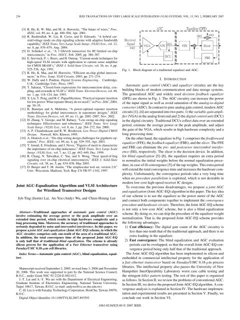
Fig. 1.<br />
Block diagram of a traditional equalizer <strong>and</strong> <strong>AGC</strong>.<br />
I. INTRODUCTION<br />
Automatic gain control (<strong>AGC</strong>) <strong>and</strong> equalizer circuitry are the key<br />
building blocks of modern communication <strong>and</strong> data storage systems.<br />
The generalized <strong>AGC</strong> <strong>and</strong> widely used decision feedback equalizer<br />
(DFE) are shown in Fig. 1. The <strong>AGC</strong> circuitry can increase the power<br />
of the input signal as well as avoid saturation of the analog-to-digital<br />
converter (ADC). In contrast to pure analog gain control, modern <strong>AGC</strong><br />
circuits [1]–[4] are separated into two parts: 1) the variable-gain amplifier<br />
(VGA) in the analog front end <strong>and</strong> 2) the digital control unit (DCU)<br />
in the digital circuitry. Traditional DCUs collect data over an extended<br />
period, estimate the average power or the peak amplitude, <strong>and</strong> adjust<br />
the gain of the VGA, which results in high hardware complexity <strong>and</strong> a<br />
long processing time.<br />
On the other h<strong>and</strong>, the equalizer in Fig. 1 comprises the feedforward<br />
equalizer (FFE), the feedback equalizer (FBE), <strong>and</strong> the slicer. The FFE<br />
<strong>and</strong> FBE can eliminate the pre- <strong>and</strong> postcursor intersymbol interference<br />
(ISI), respectively. The slicer is the decision device. In addition,<br />
for blind equalization [5]–[8], the equalizer requires an extra period<br />
to normalize the initial weights before the normal equalization procedure,<br />
in case of ill-convergence [5] of the tap weights. This extra period<br />
will extend the total convergence time <strong>and</strong> increases the hardware complexity.<br />
Unfortunately, the convergence periods take a very long time<br />
when no procedure parallelism is exploited, which is not desirable in<br />
modern low-cost high-speed receiver <strong>IC</strong> designs.<br />
To overcome the previous disadvantages, we propose a joint <strong>AGC</strong><br />
<strong>and</strong> equalization (<strong>Joint</strong> <strong>AGC</strong>-EQ) algorithm in this paper. The key idea<br />
of our scheme is to use the equalizer as the power meter of the <strong>AGC</strong><br />
<strong>and</strong> connect both components together to implement the convergence<br />
procedure <strong>and</strong> hardware circuits. Therefore, the <strong>Joint</strong> <strong>AGC</strong>-EQ scheme<br />
is not only a low-cost <strong>AGC</strong> scheme, but is also a blind equalization<br />
scheme. By doing so, we can skip the procedure of the equalizer weight<br />
normalization. That is, the proposed <strong>Joint</strong> <strong>AGC</strong>-EQ scheme provides<br />
the following advantages.<br />
1) Cost efficiency: The digital gate count of the <strong>AGC</strong> circuitry is<br />
less than one-tenth that of the traditional approach, <strong>and</strong> there is no<br />
extra loading in the equalizer.<br />
2) Fast convergence: The blind equalization <strong>and</strong> <strong>AGC</strong> evaluation<br />
periods can be overlapped, so that the overall <strong>Joint</strong> <strong>AGC</strong>-EQ convergence<br />
period being only half that of the traditional approach.<br />
The <strong>Joint</strong> <strong>AGC</strong>-EQ algorithm has been implemented in silicon <strong>and</strong><br />
embedded in commercial intellectual property for the application of<br />
a fast ethernet transceiver based on Faraday/UMC 0.18-m process<br />
libraries. The intellectual property also passes the University of New<br />
Hampshire InterOperability <strong>Lab</strong>oratory worst case cable testing <strong>and</strong><br />
the stringent killer pattern testing. The rest of this paper is organized<br />
as follows. In Section II, we review the problems of conventional <strong>AGC</strong>.<br />
In Section III, we derive the proposed <strong>Joint</strong> <strong>AGC</strong>-EQ algorithm. A convergence<br />
analysis is explained in Section IV. The hardware implementation<br />
<strong>and</strong> experimental results are presented in Section V. Finally, we<br />
conclude our work in Section VI.<br />
1063-8210/$25.00 © 2007 IEEE
IEEE TRANSACTIONS ON VERY LARGE SCALE INTEGRATION (<strong>VLSI</strong>) SYSTEMS, VOL. 15, NO. 2, FEBRUARY 2007 237<br />
Fig. 2. <strong>Joint</strong> <strong>AGC</strong>-EQ scheme based on the typical DFE.<br />
II. PROBLEMS OF CONVENTIONAL <strong>AGC</strong> SCHEMES<br />
Among numerous existing <strong>AGC</strong> schemes, we consider two major architectures:<br />
power-based <strong>AGC</strong> <strong>and</strong> peak-based <strong>AGC</strong> [1]–[4]. The accumulator<br />
or integrator in the power-based <strong>AGC</strong> [1]–[3] calculates the<br />
average power of the input signal, where the controller uses to adjust<br />
the gain of the VGA. The peak-based <strong>AGC</strong> [4] searches for the peak<br />
amplitude of the input signal over an extended period. Then, the controller<br />
adjusts the gain of the VGA to reserve a suitable margin for the<br />
maximum swing of the ADC. The disadvantages of both conventional<br />
types of <strong>AGC</strong> are summarized in the following.<br />
• Disadvantages of power-based <strong>AGC</strong>: To ensure the accuracy of<br />
a channel with a large ISI, the accumulator needs to collect input<br />
data over an extended period to estimate the power of the input<br />
signal. This is time consuming, <strong>and</strong> will slow down the overall<br />
operation. In addition, the accumulator requires large memory devices<br />
<strong>and</strong> needs to convert the amplitude values into power values.<br />
• Disadvantages of peak-based <strong>AGC</strong>: Peak-based <strong>AGC</strong> [4] is proposed<br />
for overcoming the ADC saturation. However, if an instantaneous<br />
spike or noise occurs, the selected gain could be very low.<br />
The reason is that the peak of the input signal is overestimated.<br />
To avoid this issue, averaging circuitry should be used to avoid<br />
sudden decisions resulting from noise or spikes. However, this increases<br />
the hardware complexity <strong>and</strong> lengthens the system evaluation<br />
time. Moreover, the peak-based <strong>AGC</strong> takes a long time to<br />
detect the peak if the input signal is r<strong>and</strong>om in nature.<br />
In Section III, we give the derivation of our proposed <strong>Joint</strong> <strong>AGC</strong>-EQ<br />
algorithm, which can overcome the aforementioned disadvantages.<br />
A. System Description<br />
III. PROPOSED JOINT <strong>AGC</strong>-EQ ALGORITHM<br />
The principle of a typical DFE is presented in [10]–[12]. Our proposed<br />
prototypes of the <strong>Joint</strong> <strong>AGC</strong>-EQ scheme are depicted in Fig. 2<br />
based on a typical DFE, where X(e j! ) is the power spectral density<br />
(PSD) of the VGA input signal, x(n). W(e j! ) is the PSD of the weight<br />
vector of the FFE. R(e j! ) is the PSD of the FFE input signal r(n).<br />
S(e j! ) is the PSD of the slicer input signal s(n), which is also the<br />
output signal of the FFE. We remove the ADC to simplify the notations<br />
<strong>and</strong> assume all signals of the system are in the discrete-time domain.<br />
In addition, all signals are expressed in the form of PSD for easy analysis.<br />
To avoid defocusing, we only plot the slicer, FFE, <strong>and</strong> the relative<br />
weight update circuit (WUC). The output of the FFE is fed to the slicer,<br />
where the nearest symbol will be found in the constellation space. The<br />
VGA is controlled by the DCU, so the DCU input is from the WUC of<br />
the FFE.<br />
B. Main Assumptions<br />
In traditional communication systems, the equalizer <strong>and</strong> the <strong>AGC</strong> are<br />
essentially independent both during the convergence period <strong>and</strong> in their<br />
hardware implementations. Our main idea of this paper is to integrate<br />
the <strong>AGC</strong> <strong>and</strong> equalizer into a single circuit <strong>and</strong> a single convergence<br />
process. Here, the following two assumptions are made for the further<br />
derivation.<br />
(A-1): The DCU maps the weight PSD W(e j! ) into the gain of<br />
the VGA as shown in Fig. 2. Hence, the gain of the VGA is a function<br />
of W(e j! );)<br />
that is, A(W(e j! )).<br />
The reasons for (A-1) are as follows.<br />
1) <strong>AGC</strong> should form part of an adaptive algorithm so that we can extract<br />
the power information from the equalizer in order to avoid the<br />
estimation error from ISI degradation in the traditional approach.<br />
2) To avoid using the accumulator (so as to reduce the cost) in the<br />
least mean square (LMS) algorithm [14], the weights are updated<br />
from previous weights. This means that the adaptive algorithm of<br />
the equalizer inherently employs the accumulator. This property<br />
gives us the idea to replace the accumulator in the traditional DCU<br />
by the tap weights in the equalizer.<br />
(A-2): For the desired <strong>Joint</strong> <strong>AGC</strong>-EQ, the PSD of slicer signal<br />
S(e j! ) is independent of input signal X(e j! ) after the system has<br />
converged, so the derivative of S(e j! ) relative to X(e j! ) is zero<br />
@S(e j ! )<br />
= 0: (1)<br />
@X(e j ! )<br />
The reasons for (A-2) are as follows.<br />
1) The ideal <strong>Joint</strong> <strong>AGC</strong>-EQ algorithm should be able to isolate<br />
the slicer signal from the power variation in the received signal.<br />
Hence, the PSD of slicer signal S(e j! ) is a constant for various<br />
received PSDs X(e j! ).<br />
2) Reviewing the traditional equalizer <strong>and</strong> <strong>AGC</strong> in Fig. 1, after the<br />
equalizer has converged, the PSD relationship between equalizer<br />
output S(e j! ) <strong>and</strong> equalizer input R(e j! ) is<br />
@S(e j! )<br />
=0 (2)<br />
@R(e j! )<br />
which inspires us to enlarge the relationship to that between<br />
<strong>AGC</strong>-EQ output S(e j! ) <strong>and</strong> <strong>AGC</strong>-EQ input X(e j! ) as in (1).<br />
However, (2) is not true once (1) is satisfied in the <strong>Joint</strong> <strong>AGC</strong>-EQ<br />
algorithm.<br />
C. Derivation of the <strong>Joint</strong> <strong>AGC</strong>-EQ <strong>Algorithm</strong><br />
From assumption (A-1), the PSD of the VGA output in Fig. 2 is<br />
R(e j! )=A(W(e j! )) 2 1 X(e j! ); 0
238 IEEE TRANSACTIONS ON VERY LARGE SCALE INTEGRATION (<strong>VLSI</strong>) SYSTEMS, VOL. 15, NO. 2, FEBRUARY 2007<br />
where E is the weight elastic rate (WER) that indicates the relationship<br />
between the PSD of the input signal <strong>and</strong> that of the equalizer weights.<br />
Equation (5) indicates that the dynamic range of weights is reduced<br />
by the factor (Xmin 0E 0 X0E max)=(Xmin 01 0 X01 max). Therefore, the WER<br />
plays an important role in <strong>Joint</strong> <strong>AGC</strong>-EQ, because the WER can be used<br />
to choose the suitable dynamic ranges of weights for different power<br />
ranges of input signals. Equation (5) is the solution set of the following<br />
differential equation:<br />
TABLE I<br />
STATES OF EACH COMPONENT IN (a) TRADITIONAL <strong>AGC</strong> SYSTEM<br />
AND (b) JOINT <strong>AGC</strong>-EQ SYSTEM<br />
E = 0 @W(ej! )<br />
@X(e j! ) 1 X(ej! )<br />
W (e j! ) : (6)<br />
We use (6) instead of (5) <strong>and</strong> skip the parameter e j! to simplify the<br />
following algorithm derivation. Substituting (3) <strong>and</strong> (4) into (1) yields<br />
@S<br />
@A(W )<br />
=2A(W (X)) 1<br />
@X @W(X) 1 @W(X)<br />
@X<br />
1 X 1 W + A2 (W (X))<br />
1W (X) +A 2 (W (X)) 1 X 1 @W(X) =0: (7)<br />
@X<br />
After solving the differential equations, we have<br />
A(W (e j! )) = A 0 1 W (e<br />
j! )<br />
(10E)=2E<br />
(8)<br />
where A 0 is a constant that can be considered to be the constant part<br />
of the VGA. We name this as the constant gain (CG), which is a fixed<br />
constant <strong>and</strong> independent of all other parameters in the convergence<br />
procedure.<br />
Because W (e j! ) cannot be obtained easily using equalizer hardware,<br />
we have to replace it in order to simplify the architecture. Equation<br />
(8) indicates that the gain is a function of frequency !. However,<br />
in the signal passb<strong>and</strong>, the ideal gain A(:) of the VGA should be an<br />
all-pass filter that is independent of the frequency. We, therefore, replace<br />
weight PSD W (e j! ) by its mean value<br />
W = 1<br />
2<br />
<br />
0<br />
W (e j! )d!: (9)<br />
By Parseval’s theorem [13], the mean PSD W in (9) is the same as the<br />
squared sum of tap weights<br />
W =<br />
Therefore, (8) can be further reduced to<br />
where<br />
n<br />
jw nj 2 : (10)<br />
A(w) =A 0 1 w C (11)<br />
C <br />
w <br />
(1 0 E)<br />
E<br />
n<br />
(12)<br />
w 2 n: (13)<br />
Because parameter C will build the relationship between the root of<br />
sum square (RSS) weight w <strong>and</strong> the gain of the VGA, we define it as<br />
weight-to-gain factor (WGF). Equation (11) can be easily implemented<br />
by a simple monotonic mapping function; we define the equation as the<br />
DCU mapping function. Because the central weights of (13) often dominate<br />
the RSS weight, we can only use the major terms of tap weights,<br />
instead of all filter weights, to estimate the weight PSD to decrease the<br />
hardware complexity.<br />
IV. CONVERGENCE BEHAVIOR OF THE JOINT <strong>AGC</strong>-EQ ALGORITHM<br />
A. Convergence Comparison Between <strong>Joint</strong> <strong>AGC</strong>-EQ<br />
<strong>and</strong> Traditional <strong>AGC</strong><br />
For clarity, we list the states of each component in both the traditional<br />
<strong>AGC</strong> <strong>and</strong> the <strong>Joint</strong> <strong>AGC</strong>-EQ in Table I(a) <strong>and</strong> (b), respectively. The<br />
operation procedures of both architectures are explained as follows.<br />
1) Traditional <strong>AGC</strong> System: Stage (I) in Table I(a) is the <strong>AGC</strong> evaluation<br />
stage, in which the <strong>AGC</strong> is active while the equalizer is frozen.<br />
Stage (II) is the stage of weight normalization. We briefly introduce<br />
the normalization method here. For the popular constant modulus algorithm<br />
(CMA) [9] in blind equalization, the equalizer should normalize<br />
the weights or the output power to specific values in case the weight<br />
vector is trapped in an incorrect solution. The algorithm is derived from<br />
the minimization of the following cost function [5]:<br />
J = Ef(js(n)j B 0 R B ) 2 g<br />
R B Ef(ja(n)j2B g<br />
(14)<br />
Efja(n)j B g<br />
where B is an integer (usually B =1or 2), s(n) is the slicer signal,<br />
<strong>and</strong> a(n) is the transmitted symbol at the remote end. The constant R B<br />
normalizes the equalizer weight to give zero tap-gain increments when<br />
perfect equalization is achieved. The corresponding stochastic gradient<br />
algorithm for the equalizer is<br />
w(n +1)=w(n) +r(n)e CMA (n) (15)<br />
where is the step size, w(n) is the weight vector, r(n) is the data<br />
vector, <strong>and</strong><br />
e CMA s(n))<br />
B02 (js(n)j<br />
B 0 RB): (16)<br />
e CMA (n) denotes the error signal in the CMA mode <strong>and</strong> is not the same<br />
as the error in normal decision directed equalization (DDE) [5] as in<br />
Fig. 1. At Stage (II) of Table I(a), the slicer in “CMA mode” represents<br />
that e CMA (n) updates the weights according to (16). In contrast, the<br />
slicer in “DD mode” at Stage (III) represents this error signal being the<br />
difference between the output <strong>and</strong> input signals of the slicer as shown
IEEE TRANSACTIONS ON VERY LARGE SCALE INTEGRATION (<strong>VLSI</strong>) SYSTEMS, VOL. 15, NO. 2, FEBRUARY 2007 239<br />
Fig. 3.<br />
VGA gain convergence diagram of <strong>Joint</strong> <strong>AGC</strong>-EQ embedded in typical<br />
DFE with WGF =00 5 1 <strong>and</strong> 5.<br />
in Fig. 1. The stage is the normal DDE period, <strong>and</strong> Stage (IV) is “done”<br />
state for normal receiving. Unfortunately, periods (I)–(III) take a very<br />
long time when no procedure parallelism is exploited.<br />
2) <strong>AGC</strong>-EQ System: The overall operation procedure of <strong>AGC</strong>-EQ<br />
is shown in Table I(b), where the equalizer <strong>and</strong> <strong>AGC</strong> are both active<br />
at Stage (I), so the output powers of both the equalizer <strong>and</strong> the VGA<br />
(or the ADC) converge concurrently. Normal DDE follows in Stage<br />
(II). There are only two stages before the done state of Stage (III). The<br />
VGA of Stage (II) can be active or fixed, depending on whether the<br />
gain of the VGA has converged to the optimal value at the end of Stage<br />
(I). In addition, because the weight vector in the FFE is joined with<br />
the VGA, the gain of the VGA will also settle at the optimal values<br />
before the <strong>Joint</strong> <strong>AGC</strong>-EQ process finishes. Therefore, we can avoid the<br />
<strong>AGC</strong> evaluation period in Stage (I) of Table I(a); in other words, <strong>Joint</strong><br />
<strong>AGC</strong>-EQ is seamless with a single convergence period. Thus, the total<br />
convergence time is much shorter than traditional approach.<br />
B. Simulation Results<br />
Before implementing the method on a real chip, we have to simulate<br />
the overall effects of WER (E) <strong>and</strong> WGF (C) in (6) <strong>and</strong> (12). We use<br />
the raised-cosine channel model [14] W =2:9 with an eigenvalue<br />
spread of 6.08. The signal-to-noise ratio (SNR) of the channel is 35 dB.<br />
To allow a fair comparison, we set the different CGs to equal the initial<br />
VGA outputs. The orders of FFE <strong>and</strong> FBE were 13 <strong>and</strong> 10, respectively.<br />
The step size of the normalized LMS algorithm was 2 04 . In addition,<br />
we use only the main weight to replace the RSS weight of (13). Fig. 3<br />
shows the VGA gain convergence diagrams for various values of the<br />
WGF (C) <strong>and</strong> protocol of transmitted signal is binary (PAM-2). For the<br />
special case of C =0, the receiver can be treated as using traditional<br />
blind equalization with a fixed gain for the VGA. The range of the<br />
weights can be efficiently decreased for larger WGF. The results show<br />
that the VGA can be adjusted by the main weight so as to reduce the<br />
dynamic range of the filter weights.<br />
Fig. 4(a) <strong>and</strong> (b) are the complete convergence diagrams for the traditional<br />
blind equalization <strong>and</strong> <strong>Joint</strong> <strong>AGC</strong>-EQ. The MLT-3 protocol<br />
[15] is used for the transmitted signal, <strong>and</strong> so the weight normalization<br />
period should be exploited by the CMA in traditional blind equalization.<br />
The equalizer orders <strong>and</strong> step sizes of both systems are identical.<br />
The definitions of signals <strong>and</strong> regions (I)-(IV) are also the same as in<br />
Table I(a) <strong>and</strong> (b). In summary, the required convergence time [region<br />
Fig. 4. Convergence diagram for (a) a traditional blind equalization system <strong>and</strong><br />
(b) <strong>Joint</strong> <strong>AGC</strong>-EQ with =1.<br />
(I)] of <strong>Joint</strong> <strong>AGC</strong>-EQ is only half that of traditional blind equalization<br />
[regions (I)-(II)].<br />
V. <strong>VLSI</strong> IMPLEMENTATION AND EXPERIMENTAL RESULTS<br />
A. Application of <strong>Joint</strong> <strong>AGC</strong>-EQ to Fast Ethernet<br />
We chose fast ethernet as our <strong>Joint</strong> <strong>AGC</strong>-EQ application, which was<br />
embedded in the typical DFE. The adaptive algorithm for both equalizers<br />
is the delayed LMS algorithm [11], which levers the technique of<br />
transfer delay relaxation [10] to improve the timing delay of the critical<br />
path.<br />
The final chip layout is shown in Fig. 5. The DCU comprises less<br />
than 100 logic gates, which represents a very small portion of the<br />
50 000-gate digital circuitry. Moreover, because the DCU does not
240 IEEE TRANSACTIONS ON VERY LARGE SCALE INTEGRATION (<strong>VLSI</strong>) SYSTEMS, VOL. 15, NO. 2, FEBRUARY 2007<br />
Fig. 5.<br />
<strong>Joint</strong> <strong>AGC</strong>-EQ <strong>and</strong> its related blocks in the chip layout.<br />
contain a sequential circuit (except for the latches in its output), it<br />
does not limit the operation speed. A conservative estimate is that the<br />
gate count of <strong>Joint</strong> <strong>AGC</strong>-EQ is less than one-tenth that of traditional<br />
approaches [1]–[3].<br />
B. Experimental Results<br />
Detailed measurements revealed that the BER of the chip was less<br />
than 10 012 for cable lengths between 0 <strong>and</strong> 160 m. Moreover, no received<br />
error occurred during three days of exhaustive testing for cable<br />
lengths up to 160 m. This performance not only satisfies the basic<br />
802.3u specification, but also meets a high-quality switch specification.<br />
The device also passes the University of New Hampshire InterOperability<br />
<strong>Lab</strong>oratory worst case cable testing <strong>and</strong> Killer Pattern testing<br />
[15], which has strict requirements for the swing of the input signal.<br />
After the <strong>Joint</strong> <strong>AGC</strong>-EQ algorithm converged, the dynamic power consumption<br />
was zero.<br />
VI. CONCLUSION<br />
In this paper, we propose the <strong>Joint</strong> <strong>AGC</strong>-EQ scheme, which exhibits<br />
the desirable properties of an extremely low hardware complexity <strong>and</strong><br />
our new scheme can avoid the weight initialization period <strong>and</strong> can<br />
shorten the overall convergence time. <strong>Joint</strong> <strong>AGC</strong>-EQ is silicon-proven<br />
for the application of a fast ethernet transceiver using Faraday/UMC<br />
0.18-m cell libraries, for which the performance is better than the<br />
802.3u specification <strong>and</strong> the BER is less than 10 012 for cable lengths<br />
up to 160 m.<br />
REFERENCES<br />
[1] W. Eberle et al., “Behavioral modeling <strong>and</strong> simulation of a mixed<br />
analog/digital automatic gain control loop in a 5 GHz WLAN receiver,”<br />
in Proc. Des., Autom. Testing Eur. Conf. Exhibition, 2003, pp.<br />
642–647.<br />
[2] H. O. Elwan, T. B. Tarim, <strong>and</strong> M. Ismail, “A digitally controlled<br />
dB-linear CMOS <strong>AGC</strong> for low voltage mixed signal applications,” in<br />
Proc. Circuits Syst. Midw. Symp., 1998, pp. 423–425.<br />
[3] G. S. Kang <strong>and</strong> M. L. Lidd, “Automatic gain control,” in Proc. IEEE<br />
Int. Conf. Acoust., Speech Signal Process., 1984, pp. 120–124.<br />
[4] K. Chopra <strong>and</strong> D. D. Woods, “A maximum likehood peak detecting<br />
channel,” IEEE Trans. Magn., vol. 27, no. 6, pp. 4819–4821, Nov.<br />
1991.<br />
[5] S. Haykin, Blind Deconvolution. Englewood Cliffs, NJ: Prentice-Hall,<br />
1994.<br />
[6] G. P. John, Digital Communications. New York: McGraw-Hill, 2001.<br />
[7] D. N. Godard, “Self-recovering equalization <strong>and</strong> carrier tracking in two<br />
dimensional data communication systems,” IEEE Trans. Commun.,<br />
vol. COM-28, no. 11, pp. 1867–1875, Nov. 1980.<br />
[8] A. Benveniste <strong>and</strong> G. Goursat, “Blind equalizers,” IEEE Trans.<br />
Commun., vol. COM-32, no. 8, pp. 871–883, Aug. 1984.<br />
[9] V. Weerackody <strong>and</strong> S. A. Kassam, “Dual-mode type algorithms for<br />
blind equalization,” IEEE Trans. Commun., vol. 42, no. 1, pp. 22–28,<br />
Jan. 1994.<br />
[10] N. R. Shanbhag <strong>and</strong> K. K. Parhi, “Pipelined adaptive DFE architectures<br />
using relaxed look-ahead,” IEEE Trans. Signal Process., vol. 43, no. 6,<br />
pp. 1368–1385, Jun. 1995.<br />
[11] G. Long, F. Ling, <strong>and</strong> J. G. Proakis, “The LMS algorithm with delayed<br />
coefficient adaptation,” IEEE Trans. Acoust. Speech Signal Process.,<br />
vol. 37, no. 9, pp. 1397–1405, Sep. 1989.<br />
[12] B. Widrow <strong>and</strong> S. D. Stearns, Adaptive Signal Processing. Englewood<br />
Cliffs, NJ: Prentice-Hall, 1985.<br />
[13] A. V. Oppenheim, Discrete-Time Signal Processing. Englewood<br />
Cliffs, NJ: Prentice-Hall, 1989.<br />
[14] S. Haykin, Adaptive Filter Theory. Englewood Cliffs, NJ: Prentice-<br />
Hall, 1991.<br />
[15] Univ. New Hampshire InterOperability <strong>Lab</strong>., “100Base-TX Testsuite,”<br />
2006 [Online]. Available: http://www.iol.unh.edu/testsuites/fe/pmd.html<br />
Customization of Arbitration Policies <strong>and</strong> Buffer<br />
Space Distribution Using Continuous-Time<br />
Markov Decision Processes<br />
Sankalp S. Kallakuri <strong>and</strong> Alex Doboli<br />
Abstract—This paper presents a stochastic approach for bus arbiter<br />
design. Arbiter design includes policy design, buffer insertion, <strong>and</strong> optimal<br />
buffer sizing. The methodology uses continuous-time Markov decision<br />
processes (CTMDPs) to get optimal arbitration policies <strong>and</strong> buffer space<br />
distribution. The mathematical formulation of this problem in terms of<br />
a CTMDP framework leads to a linear programming problem for bus<br />
architectures without bridges, <strong>and</strong> to a nonlinear formulation for bus<br />
architectures with bridges. In the second case, the methodology splits the<br />
nonlinear problem into several smaller, linear subsystems by introducing<br />
buffers at the bridges, <strong>and</strong> then solves the linear subsystems. In our<br />
experiments, we found that stochastic policies provide efficient arbitration<br />
for bus architectures with redundant buses for communication between<br />
processors. The size of buffers in some cases was reduced by 90%, <strong>and</strong><br />
by 50% in the average sense. Data loss was reduced by 20% to 50% with<br />
redistribution of the buffer space.<br />
Index Terms—Bus arbitration, continuous time Markov decision processes<br />
(CTMDPs), stochastic modeling.<br />
I. INTRODUCTION<br />
Design of the communication subsystem for SoCs is a fast growing<br />
field of research with complex multiprocessor systems being developed<br />
[1], [7], [10]. It is a pertinent issue in the development of flexible,<br />
scalable, fast, <strong>and</strong> low power SoCs, as the communication subsystem<br />
Manuscript received October 4, 2004; revised February 22, 2006 <strong>and</strong> May 2,<br />
2006.<br />
The authors are with the Department of Electrical <strong>and</strong> Computer Engineering,<br />
Stony Brook University, Stony Brook, NY, 11794-2350 USA (e-mail:<br />
elsanky@ece.sunysb.edu; adoboli@ece.sunysb.edu).<br />
Digital Object Identifier 10.1109/T<strong>VLSI</strong>.2007.895003<br />
1063-8210/$25.00 © 2007 IEEE

![On [n, n - 1] convolutional codes with low trellis complexity ...](https://img.yumpu.com/45854741/1/190x245/on-n-n-1-convolutional-codes-with-low-trellis-complexity-.jpg?quality=85)