AMSV Newsletter 2014
AMSV Newsletter 2014
AMSV Newsletter 2014

You also want an ePaper? Increase the reach of your titles
YUMPU automatically turns print PDFs into web optimized ePapers that Google loves.
Normalized Power-delay product<br />
In TVLSI 2015<br />
Energy Optimized Sub-threshold VLSI Logic Family with Unbalanced<br />
Pull-up/down Network and Inverse-Narrow-Width Techniques<br />
Ming-Zhong Li, Chio-In Ieong, Man-Kay Law, Pui-In Mak, Mang-I Vai, Sio-Hang Pun and Rui P.<br />
Martins<br />
From Biomedical IC research line<br />
(Accepted in <strong>2014</strong>)<br />
Motivation<br />
Ultra-low-energy biomedical applications have<br />
urged the development of a sub-threshold VLSI<br />
logic family in standard CMOS. Instead of the<br />
traditionally preferred balanced pull-up (PU) and<br />
pull-down (PD) network approach in logic cell<br />
design, this work proposes an unbalanced pullup/down<br />
network together with an inversenarrow-width<br />
technique to improve the operating<br />
speed of the individual logic cell. Effective logical<br />
efforts save both power and die area in the process<br />
of device sizing and topology optimization.<br />
Three experimental 14-tap 8-bit finite impulse<br />
response (FIR) filters optimized for ultra-lowvoltage<br />
operation were fabricated in 0.18-μm<br />
CMOS. Measurements show that the optimized<br />
0.45-V and 0.6-V libraries achieve minimum energy<br />
operations at 100 kHz, with a Figure-of-<br />
Merit (FoM) of 0.365 (at 0.31 V) and 0.4632 (at<br />
0.39 V), respectively. They correspond to<br />
35.96% and 18.74% improvements, and the<br />
overall performances are well comparable with<br />
the state-of-the-art.<br />
Power-delay product (J)<br />
10 -17<br />
10 -18<br />
10 -19<br />
Architecture<br />
10 -15 Operating<br />
with balancing<br />
w/o balancing<br />
frequency limit<br />
10 -16 difference<br />
(unbalanced)<br />
40%<br />
30%<br />
20%<br />
10%<br />
0%<br />
10 3 10 4 10 5 10 6<br />
Frequency (Hz)<br />
10 7<br />
Difference in power-delay product<br />
4.0<br />
3.2<br />
2.4<br />
1.6<br />
WNMOS = 0.88 mm<br />
WNMOS = 0.66 mm<br />
WNMOS = 0.44 mm<br />
WNMOS = 0.22 mm<br />
0.8<br />
0.2 0.4 0.6 0.8 1 1.2 1.4<br />
PMOS Width (mm)<br />
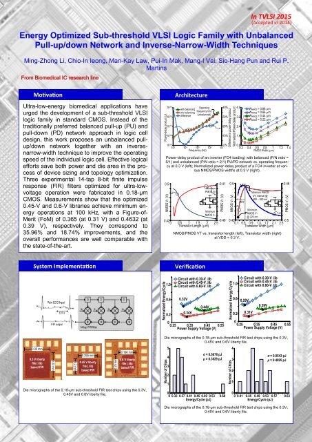
Power-delay product of an inverter (FO4 loading) with balanced (P/N ratio =<br />
5/1) and unbalanced (P/N ratio = 2/1) PU/PD network vs. operating frequency<br />
at 0.3 V (left); Normalized power-delay product of a FO4 inverter at various<br />
NMOS/PMOS widths at 0.3 V (right).<br />
0.5<br />
NMOS VT (V)<br />
Minimum<br />
PMOS |VT|<br />
-0.41<br />
PMOS VT (V)<br />
0.5<br />
Minimum PMOS<br />
|VT| interval @<br />
400 – 590 nm<br />
-0.46<br />
Minimum<br />
Minimum<br />
NMOS VT<br />
NMOS VT<br />
@ 220 nm<br />
0.42<br />
-0.49 0.42<br />
-0.5<br />
0 0.5 1 1.5 2 2.5<br />
0.1 0.5 0.9 1.3 1.7 2.1 2.5<br />
Transistor Length (mm)<br />
Transistor Width (mm)<br />
NMOS/PMOS VT vs. transistor length (left); Transistor width (right)<br />
at VDD = 0.3 V.<br />
NMOS VT (V)<br />
INW<br />
PMOS VT (V)<br />
System Implementation<br />
Verification<br />
Normalized Energy/Cycle<br />
1.0<br />
0.6<br />
0.2<br />
Circuit with 0.30-V .lib<br />
Circuit with 0.45-V .lib<br />
Circuit with 0.60-V .lib<br />
0.32V<br />
0.44V<br />
0.34V<br />
0<br />
0.25 0.35 0.45 0.55<br />
Power Supply Voltage (V)<br />
Normalized Energy/Cycle<br />
Circuit with 0.30-V .lib<br />
Circuit with 0.45-V .lib<br />
1.0<br />
Circuit with 0.60-V .lib<br />
0.6<br />
0.28V<br />
0.39V<br />
0.2 0.31V<br />
0<br />
0.25 0.35 0.45 0.55<br />
Power Supply Voltage (V)<br />
0.35 mm<br />
0.3 V liberty<br />
file (.lib)<br />
based FIR<br />
0.33 mm<br />
0.2 mm<br />
0.265 mm<br />
0.45 V liberty<br />
file (.lib)<br />
based FIR<br />
0.25 mm<br />
0.196 mm<br />
0.6 V liberty<br />
file (.lib)<br />
based FIR<br />
Die micrographs of the 0.18-µm sub-threshold FIR test chips using the 0.3V,<br />
0.45V and 0.6V liberty file.<br />
Die micrographs of the 0.18-µm sub-threshold FIR test chips using the 0.3V,<br />
0.45V and 0.6V liberty file.<br />
Number of Chips<br />
5<br />
4<br />
3<br />
2<br />
1<br />
σ = 0.0678 pJ<br />
μ = 0.3829 pJ<br />
0<br />
0 0.33 0.37 0.41 0.45 0.49 0.53 0.60<br />
Energy/Cycle (pJ)<br />
Number of Chips<br />
4<br />
3<br />
2<br />
1<br />
σ = 0.0543 pJ<br />
μ = 0.4995 pJ<br />
0<br />
0 0.41 0.45 0.49 0.53 0.57 0.63<br />
Energy/Cycle (pJ)<br />
Die micrographs of the 0.18-µm sub-threshold FIR test chips using the 0.3V,<br />
0.45V and 0.6V liberty file.