AMSV Newsletter 2014
AMSV Newsletter 2014
AMSV Newsletter 2014

Create successful ePaper yourself
Turn your PDF publications into a flip-book with our unique Google optimized e-Paper software.
State Key Lab of Analog and Mixed-Signal VLSI (SKL AMS-VLSI)<br />
<strong>Newsletter</strong><br />
Motto: “Locally, from (World) Quality towards (National) Quantity”<br />
座 右 銘 : 立 足 本 土 、 人 才 培 養 , 以 世 界 級 質 量 創 建 國 家 級 規 模<br />
Year 4<br />
No . 4<br />
<strong>2014</strong> Milestones<br />
March 2015<br />
Co-Funded by<br />
Macao Science and Technology<br />
Development Fund (FDCT)<br />
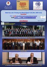
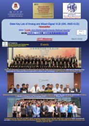
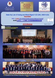
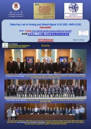
Events<br />
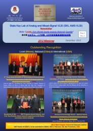
President Xi Jinping visited UM, and listened to the report of SKL (<strong>AMSV</strong>-VLSI) research achievements. President Xi<br />
mentioned that was happy to see the self-developed state-of-the-art leading chips and encouraged our team to contribute<br />
further to China high-level strategy policy of "Leading by Innovation" - as quoted by online Chinese Media.<br />
At Macao Science and Technology Awards presented this<br />
year, SKL AMS-VLSI won two 2nd and one 3rd prizes in<br />
the Technological Invention Award category. Also, Technology<br />
Development Award was granted to 3 PhD students<br />
and 1 Master Student from SKL AMS-VLSI<br />
SKL AMS-VLSI awarded "Excellence in INNOVATION"<br />
by Business Awards of Macau on Nov-<strong>2014</strong>
900MS/s 11b ADC (65nm)<br />
State-of-the-Art Chips - Designed and Tested in <strong>2014</strong> (9 chips)<br />
DCSP Chips<br />
Integrated Power Chips<br />
A 123-Phase DC-DC Converter-Ring with Fast-DVS for<br />
Microprocessors (65nm)<br />
430μm<br />
Ch.1<br />
Ch.2<br />
2 nd -stage<br />
1 st -stage<br />
340μm<br />
CLK Gen.<br />
Output Buffers<br />
Wireless Chips<br />
High efficient 5GHz ADC (65nm)<br />
A VCO-based Switched-Capacitor DC-DC Converter with Segment<br />
Frequency Modulation Control for Fast Recovery (65nm)<br />
BME (Biomedical Engineering) Chips<br />
Ultra-high Area Efficient and Low-<br />
Power Wireless Receiver (65nm)<br />
Single Chip Solar Energy<br />
Harvesting IC (180nm)<br />
Supply Modulated Micro-stimulator<br />
with Energy Recycling (180nm)<br />
ISSCC 2015<br />
µNMR Transceiver for Chemical/Biological Diagnosis and<br />
Ultra-low Power Wavelet Shrinkage ECG Processor (180nm)<br />
Optogenetic Frontend IC and Nested-<br />
Current-Mirror Amplifier (180nm)<br />
Four PhD students and one assistant professor from the University of Macau (UM) State Key Laboratory of Analog<br />
and Mixed-Signal VLSI (AMS-VLSI Lab) and Faculty of Science and Technology attended the Institute of Electrical<br />
and Electronics Engineer’s (IEEE) 62 nd International Solid-State Circuits Conference (ISSCC) in February 2015,<br />
which is considered the ‘Chip Olympics’, the most competitive conference in the field of chip design.<br />
The 6 papers from UM were "A 5.5mW 6b 5GS/s 4-times<br />
Interleaved 3b/cycle SAR ADC in 65nm CMOS", "A Multi-<br />
Step Multi-Sample µNMR Relaxometer Using Inside-Magnet<br />
Digital Microfluidics and a Butterfly-Coil-Input CMOS<br />
Transceiver", "A 12b 180MS/s 0.068mm 2 Full-Calibration-<br />
Integrated Pipelined-SAR ADC", "A 123-Phase DC-DC<br />
Converter-Ring with Fast-DVS for Microprocessors", "A<br />
0.028mm 2 11mW Single-Mixing Blocker-Tolerant Receiver<br />
with Double-RF N-Path Filtering, S 11 Centering, +13dBm<br />
OB-IIP 3 and 1.5-to-2.9dB NF", and "A 2-/3-Phase Fully-<br />
Integrated Switched-Capacitor DC-DC Converter in Bulk-<br />
CMOS for Energy-Efficient Digital Circuits With 14% Efficiency<br />
Improvement". There included 2 Pre-Doctoral<br />
Achievement Awards and 2 Student Research Previews.<br />
UM’s 1st book in<br />
Power Electronics<br />
UM PhD graduates to join the world’s No 1 mobile chip maker and Asia’s largest<br />
fabless IC design company<br />
Four PhD graduates from SKL AMS-VLSI recently<br />
passed their oral defenses, with external examiners<br />
unanimously praising their works for<br />
reaching world-class standards. The 4 new doctors<br />
are Un Ka-Fai, Yan Zushu, Lin Zhicheng,<br />
and Lin Fujian. Two of them have received job<br />
contracts from Qualcomm in the United States,<br />
which is the world’s No 1 mobile chip maker. One<br />
has joined Mediatek in Singapore, which is<br />
Asia’s largest fabless IC design company and<br />
ranks No 4 in the world. The last has decided to<br />
stay at UM as a post-doctoral researcher.<br />
US Patents granted in <strong>2014</strong><br />
1. C. Shi, M. K. Law and A. Bermak, “Method and Apparatus for Energy Harvesting using CMOS Sensor”, US<br />
Patent, US8629386 B2, Jan. 14, <strong>2014</strong>.<br />
2. Chi-Hang Chan, Yan Zhu, U-Fat Chio, Sai-Weng Sin, Seng-Pan U and Martins, R.P., "Comparator and<br />
Calibration Thereof", US Patent, US8829942 B2, Sept. 9, <strong>2014</strong>.
Selected works from each research line<br />
In ESSCIRC <strong>2014</strong><br />
An 11b 900 MS/s Time-Interleaved Sub-ranging Pipelined-SAR ADC<br />
[Best Paper Award]<br />
Yan Zhu, Chi-Hang Chan, Seng-Pan U, Rui P. Martins<br />
From Data Conversion and Signal Processing research line<br />
Motivation<br />
The highly Time-Interleaved(TI) SAR ADC with<br />
timing-calibration obtains the best power efficiency<br />
for the GHz speed goal, which removes<br />
the power and accuracy trade-off in the clock<br />
generator. However, the calibration sensitivity is<br />
limited by the type of input signal or the other<br />
non-idealities among sub-SAR ADCs such as<br />
reference noise, offset and gain mismatches.<br />
The skew calibration achieves better than 63dB<br />
SFDR in a TI-SAR ADC with GHz sampling rate<br />
and 10b resolution, while the calibration power<br />
from offset, gain and timing occupies near 50%<br />
total ADC power. This paper presents an 11b TI<br />
-sub-ranging pipelined-SAR ADC that achieves<br />
a maximum 1.1GS/s sampling rate with competitive<br />
power-efficiency as compared with the<br />
timing-calibrated TI-SAR ADCs. We propose the<br />
optimization Based on ADC’s sampling frontend<br />
for better SFDR by using the proposed<br />
channel-selection-embedded bootstrap rather<br />
than timing-calibration.<br />
Architecture<br />
Channel Selection Embedded (CSE)<br />
Bootstrap Circuit<br />
Φ 1(Φ 2)<br />
ΦM<br />
Φ1<br />
Vin<br />
Φ2<br />
Vdd<br />
2 Main S/H<br />
channels<br />
CSE<br />
Bootstrap<br />
A1<br />
CSE<br />
Bootstrap<br />
A2<br />
CF<br />
CF<br />
Vin<br />
6 Sub-S/H channels<br />
Φ1,1<br />
Φ1,2<br />
Φ1,3<br />
Φ2,1<br />
Φ2,2<br />
Φ2,3<br />
VB1(B2)<br />
DAC<br />
DAC<br />
DAC<br />
DAC<br />
DAC<br />
DAC<br />
Bootstraped<br />
switch<br />
M4<br />
A1(A2) M3<br />
V dd<br />
M1<br />
Φ P1(Φ P2)<br />
M2<br />
Φ s(Φ s)<br />
Φ M<br />
System Implementation<br />
Power (dB)<br />
System Implementation<br />
Gain Mismatches offset Mismatches<br />
0<br />
fs=900MS/s, fin=11MHz<br />
HD3<br />
HD2<br />
HD4<br />
HD5 HD8<br />
-100<br />
Verification<br />
Power (dB)<br />
0 0.1 0.2 0.3 0.4 0.5<br />
Normalized Frequency (fin / fs)(decimate by 25)<br />
Skew/Gain Mismatches offset Mismatches<br />
0<br />
SNR = 51.7 dB, SNDR = 51.5 dB, fs=900MS/s, fin=431MHz<br />
SFDR = 65.9 dB, THD = -64.3 dB<br />
HD3<br />
HD8 HD2<br />
-100<br />
0 0.1 0.2 0.3 0.4 0.5<br />
Normalized Frequency (fin / fs)(decimate by 25)<br />
SNDR & SFDR (dB)<br />
70<br />
68<br />
66<br />
64<br />
62<br />
60<br />
58<br />
56<br />
54<br />
52<br />
50<br />
SFDR<br />
SNR<br />
SNDR<br />
CLK Jitter 650fs<br />
10 100 200 300 400 500<br />
Input frequency (MHz) @f s=900MS/s<br />
Verification<br />
[1]<br />
[2]<br />
[3]<br />
[8]<br />
ISSCC’14 ISSCC’14 JSSCC’13 VLSI’13<br />
This Work<br />
Architecture<br />
Technology (nm)<br />
TI-SAR<br />
40<br />
TI-SAR<br />
65<br />
TI-SAR<br />
65<br />
Pipeline<br />
65<br />
TI-Pipelined-SAR<br />
65<br />
Resolution (bit)<br />
Sampling Rate (MS/s)<br />
Supply Voltage (V)<br />
10<br />
1.62<br />
1.1<br />
10<br />
1<br />
1<br />
10<br />
2.8<br />
1<br />
10<br />
0.8<br />
1.2<br />
11<br />
0.9<br />
1.2/1.2<br />
11<br />
1.1<br />
1.2/1.3<br />
Input Swing (Vp-p)<br />
1<br />
N/A N/A<br />
1.8 1.2 1.2<br />
SNDR @DC (dB)<br />
SNDR @Nyq. (dB)<br />
51<br />
48<br />
53.5<br />
51.2<br />
53.5<br />
51.2<br />
51<br />
48<br />
57.6<br />
51.5<br />
56.2<br />
50.7<br />
SFDR @Nyq. (dB) 62 60 55<br />
N/A 65.9 64<br />
DNL/INL (LSB)<br />
N/A 0.1/0.1 N/A 0.7/1.8 0.66/1.5 0.69/1.6<br />
Area (mm 2 )<br />
0.83<br />
0.78<br />
1.7<br />
0.18<br />
0.15<br />
Power (mW)<br />
71<br />
19.8<br />
44.6<br />
19 15.5 18<br />
FoM @DC (fJ/conv.step) 150<br />
51 56<br />
53 28 32<br />
FoM @Nyq. (fJ/conv.step) 210<br />
62 78<br />
71 56 58<br />
Require Timing Correction Yes Yes Yes No No<br />
Calibration (on-chip)<br />
Offset, gain,<br />
time<br />
Offset Offset, time No Offset
Normalized Power-delay product<br />
In TVLSI 2015<br />
Energy Optimized Sub-threshold VLSI Logic Family with Unbalanced<br />
Pull-up/down Network and Inverse-Narrow-Width Techniques<br />
Ming-Zhong Li, Chio-In Ieong, Man-Kay Law, Pui-In Mak, Mang-I Vai, Sio-Hang Pun and Rui P.<br />
Martins<br />
From Biomedical IC research line<br />
(Accepted in <strong>2014</strong>)<br />
Motivation<br />
Ultra-low-energy biomedical applications have<br />
urged the development of a sub-threshold VLSI<br />
logic family in standard CMOS. Instead of the<br />
traditionally preferred balanced pull-up (PU) and<br />
pull-down (PD) network approach in logic cell<br />
design, this work proposes an unbalanced pullup/down<br />
network together with an inversenarrow-width<br />
technique to improve the operating<br />
speed of the individual logic cell. Effective logical<br />
efforts save both power and die area in the process<br />
of device sizing and topology optimization.<br />
Three experimental 14-tap 8-bit finite impulse<br />
response (FIR) filters optimized for ultra-lowvoltage<br />
operation were fabricated in 0.18-μm<br />
CMOS. Measurements show that the optimized<br />
0.45-V and 0.6-V libraries achieve minimum energy<br />
operations at 100 kHz, with a Figure-of-<br />
Merit (FoM) of 0.365 (at 0.31 V) and 0.4632 (at<br />
0.39 V), respectively. They correspond to<br />
35.96% and 18.74% improvements, and the<br />
overall performances are well comparable with<br />
the state-of-the-art.<br />
Power-delay product (J)<br />
10 -17<br />
10 -18<br />
10 -19<br />
Architecture<br />
10 -15 Operating<br />
with balancing<br />
w/o balancing<br />
frequency limit<br />
10 -16 difference<br />
(unbalanced)<br />
40%<br />
30%<br />
20%<br />
10%<br />
0%<br />
10 3 10 4 10 5 10 6<br />
Frequency (Hz)<br />
10 7<br />
Difference in power-delay product<br />
4.0<br />
3.2<br />
2.4<br />
1.6<br />
WNMOS = 0.88 mm<br />
WNMOS = 0.66 mm<br />
WNMOS = 0.44 mm<br />
WNMOS = 0.22 mm<br />
0.8<br />
0.2 0.4 0.6 0.8 1 1.2 1.4<br />
PMOS Width (mm)<br />
Power-delay product of an inverter (FO4 loading) with balanced (P/N ratio =<br />
5/1) and unbalanced (P/N ratio = 2/1) PU/PD network vs. operating frequency<br />
at 0.3 V (left); Normalized power-delay product of a FO4 inverter at various<br />
NMOS/PMOS widths at 0.3 V (right).<br />
0.5<br />
NMOS VT (V)<br />
Minimum<br />
PMOS |VT|<br />
-0.41<br />
PMOS VT (V)<br />
0.5<br />
Minimum PMOS<br />
|VT| interval @<br />
400 – 590 nm<br />
-0.46<br />
Minimum<br />
Minimum<br />
NMOS VT<br />
NMOS VT<br />
@ 220 nm<br />
0.42<br />
-0.49 0.42<br />
-0.5<br />
0 0.5 1 1.5 2 2.5<br />
0.1 0.5 0.9 1.3 1.7 2.1 2.5<br />
Transistor Length (mm)<br />
Transistor Width (mm)<br />
NMOS/PMOS VT vs. transistor length (left); Transistor width (right)<br />
at VDD = 0.3 V.<br />
NMOS VT (V)<br />
INW<br />
PMOS VT (V)<br />
System Implementation<br />
Verification<br />
Normalized Energy/Cycle<br />
1.0<br />
0.6<br />
0.2<br />
Circuit with 0.30-V .lib<br />
Circuit with 0.45-V .lib<br />
Circuit with 0.60-V .lib<br />
0.32V<br />
0.44V<br />
0.34V<br />
0<br />
0.25 0.35 0.45 0.55<br />
Power Supply Voltage (V)<br />
Normalized Energy/Cycle<br />
Circuit with 0.30-V .lib<br />
Circuit with 0.45-V .lib<br />
1.0<br />
Circuit with 0.60-V .lib<br />
0.6<br />
0.28V<br />
0.39V<br />
0.2 0.31V<br />
0<br />
0.25 0.35 0.45 0.55<br />
Power Supply Voltage (V)<br />
0.35 mm<br />
0.3 V liberty<br />
file (.lib)<br />
based FIR<br />
0.33 mm<br />
0.2 mm<br />
0.265 mm<br />
0.45 V liberty<br />
file (.lib)<br />
based FIR<br />
0.25 mm<br />
0.196 mm<br />
0.6 V liberty<br />
file (.lib)<br />
based FIR<br />
Die micrographs of the 0.18-µm sub-threshold FIR test chips using the 0.3V,<br />
0.45V and 0.6V liberty file.<br />
Die micrographs of the 0.18-µm sub-threshold FIR test chips using the 0.3V,<br />
0.45V and 0.6V liberty file.<br />
Number of Chips<br />
5<br />
4<br />
3<br />
2<br />
1<br />
σ = 0.0678 pJ<br />
μ = 0.3829 pJ<br />
0<br />
0 0.33 0.37 0.41 0.45 0.49 0.53 0.60<br />
Energy/Cycle (pJ)<br />
Number of Chips<br />
4<br />
3<br />
2<br />
1<br />
σ = 0.0543 pJ<br />
μ = 0.4995 pJ<br />
0<br />
0 0.41 0.45 0.49 0.53 0.57 0.63<br />
Energy/Cycle (pJ)<br />
Die micrographs of the 0.18-µm sub-threshold FIR test chips using the 0.3V,<br />
0.45V and 0.6V liberty file.
Voltage<br />
Voltage<br />
In American Institute of Physics – Advances <strong>2014</strong><br />
Natural Discharge after Pulse and Cooperative Electrodes to<br />
Enhance Droplet Velocity in Digital Microfluidics<br />
Tianlan Chen, Cheng Dong, Jie Gao, Yanwei Jia, Pui-In Mak, Mang-I Vai, and Rui P. Martins<br />
From Multidisciplinary Research Area<br />
Motivation<br />
Architecture<br />
Digital Microfluidics (DMF) is a promising technology<br />
for biological/chemical micro-reactions<br />
due to its distinct droplet manageability via electronic<br />
automation, but the limited velocity of<br />
droplet transportation has hindered DMF from<br />
utilization in high throughput applications.<br />
In this paper, by adaptively fitting the actuation<br />
voltages to the dynamic motions of droplet<br />
movement under real-time feedback monitoring,<br />
two control-engaged electrode-driving techniques:<br />
Natural Discharge after Pulse (NDAP)<br />
and Cooperative Electrodes (CE) are proposed.<br />
They together lead to, for the first time, enhanced<br />
droplet velocity with lower root mean<br />
square voltage value.<br />
uα<br />
uβ<br />
uβ’<br />
0<br />
uα<br />
uβ<br />
uβ’<br />
0<br />
HV period<br />
tα’<br />
LV period<br />
tβ<br />
tα<br />
1 st electrode<br />
tthc<br />
tths<br />
tths<br />
Time<br />
NDAP<br />
2 nd electrode<br />
NDAP + CE<br />
(a)<br />
(b)<br />
uα<br />
0<br />
uα<br />
0<br />
Sketches of four possible electrode-driving schemes for droplet movements<br />
over two electrodes: (a) Natural Discharge after Pulse (NDAP): The highvoltage<br />
(HV) period lasts shorter, while the low-voltage (LV) under natural<br />
discharge lasts longer with short pulse recharging periodically. (b) DC signal.<br />
(c) NDAP with cooperative electrodes (CE) overlaps the charging time of<br />
neighboring electrodes. (d) DC plus CE driving. (e) Droplet moving toward<br />
two target electrodes and location of the two thresholds on the first target<br />
electrode. The electrode was grounded when the charging was done in all<br />
schemes.<br />
tthc<br />
tths<br />
tths<br />
Time<br />
DC<br />
DC + CE<br />
(c)<br />
(d)<br />
thc<br />
ths<br />
1st<br />
2nd<br />
(e)<br />
Result I<br />
Result II<br />
(a) Velocity comparison of NDAP signals with different and DC. NDAP with<br />
13-ms to 100-ms has average velocities higher than DC signal. (b) Video<br />
frames of a droplet actuated by NDAP and DC crossing 2 electrodes<br />
(Multimedia view). Video was captured by a high speed camera (Nikon V2),<br />
which has a maximum frame rate up to 1200 frames/second (resolution 320<br />
x 120 pixels). A LED light was set in the same frame to light on when the<br />
electrode was being charged. Individual frames extracted from the videos<br />
were analyzed by the image processing software Image J to obtain the<br />
v droplet.<br />
Comparison between the proposed (NDAP + CE and high-speed feedback)<br />
and classical (DC) schemes for droplet movements in a long run of 3 s: (a)<br />
Droplet successfully moved across 12 electrodes when it was controlled by<br />
the proposed scheme. The path of the droplet’s center had been shortened<br />
at electrode No. 6 by CE, which charged electrode No. 7 before the droplet<br />
reached electrode No. 6, resulting in an upward move of droplet in advance.<br />
The whole droplet transportation was recorded in video (Multimedia view).<br />
(b) Droplet failed to complete movement in 3 s due to its lower speed. The<br />
moving path was close to the right angle at the two corners. The whole<br />
droplet transportation was recorded in video (Multimedia view). (c) Instantaneous<br />
velocity of the droplet moving across the electrodes. As expected,<br />
droplet controlled by the proposed scheme moved across electrode No. 6-7-<br />
8 using a much shorter time than that of the classical procedure.
In Royal Society of Chemistry - Analyst <strong>2014</strong><br />
NMR-DMF: A Modular Nuclear Magnetic Resonance–Digital<br />
Microfluidics System for Biological Assays<br />
Ka-Meng Lei, Pui-In Mak, Man-Kay Law, and Rui P. Martins<br />
From Multidisciplinary Research Area<br />
Motivation<br />
Architecture I<br />
We present a modular nuclear magnetic resonance–digital<br />
microfluidics (NMR-DMF) system<br />
as a portable diagnostic platform for miniaturized<br />
biological assays.<br />
With increasing numbers of combination between<br />
designed probes and a specific target,<br />
NMR becomes an accurate and rapid assay tool<br />
capable of detecting particular kinds of proteins,<br />
DNAs, bacteria and cells with a customized<br />
probe quantitatively.<br />
Traditional sample operation (e.g., manipulation<br />
and mixing) relied heavily on human efforts. We<br />
herein propose a modular NMR-DMF system to<br />
allow electronic automation of multi-step reaction-screening<br />
protocols.<br />
The overall schematics and operations of the NMR-DMF system. (a) The<br />
placement of the DMF chip, magnet, RF coil and PCB board in 3D view. Benefit<br />
from the plane-parallel magnetic field generated by the figure-8 shaped coil,<br />
the NMR system can be effectively integrated into the DMF system; (b) Schematics<br />
of the NMR Electronics. The transmitter which is formed by the digital<br />
logics such as flip flops is used to excite the hydrogen atom. On the receiver<br />
part, the capacitor together with the RF-coil (fabricated figure-8 shaped coil)<br />
forms a LC tank to provide passive gain enhancing of the system’s sensitivity.<br />
The signal is then amplified and down converted to f IF (intermediate frequency)<br />
and fed to the external filters and oscilloscope; (c) The filtered results from the<br />
PCB are captured by the oscilloscope for easier demonstration purpose.<br />
Waveforms are then analysed and the spin-spin relaxation time (T 2) is fitted by<br />
the algorithm written in MATLAB; (d) The photograph of the DMF chip and<br />
structure of the DMF platform. The droplets are squeezed between the top and<br />
bottom planes and surrounded by silicone oil; (e) The detection mechanism of<br />
the NMR-DMF system. The target-specific magnetic nanoparticles, which act<br />
as probes, are placed on the sensing site initially (in purple). The samples at<br />
other electrodes (in cyan) will be transported to the sensing site and mixed with<br />
the probes to perform NMR assays automatically by applying voltage on corresponding<br />
electrodes. Without the target, the probes stay monodispersed and<br />
will have a longer T 2. Otherwise, the target and probes will form clusters by<br />
forming bonds between each other and the T 2 will be decreased.<br />
Architecture II<br />
Result<br />
(a) Plot of unit magnetic field in y-direction of the 14-turn figure-8 shaped coil<br />
along z-axis. The magnetic field is stronger on the coil surface (1.8 mT) and<br />
starts to decrease above the coil. Inset shows the photograph of the 14-turn<br />
figure-8 shaped coil; (b) The magnetic flux lines of the simulated 14-turn<br />
figure-8 shaped coil. The magnetic fluxes are still pointing in the z-direction<br />
at the centres of each coil. However, between the two coils, the magnetic<br />
flux is pointing in the y-direction, generating plane-parallel magnetic flux. (c)<br />
Plane-parallel magnetic flux density map of the 14-turn figure-8 shaped coil<br />
at z = 0.6 mm (depth of the ITO glass). The sensing region, which is defined<br />
as the area have a plane-parallel magnetic flux density larger than 50% its<br />
peak value (1.43 mT) is located between the centers of two coils and has a<br />
shape of circle with diameter around 4.2 mm.<br />
(a) Illustration of droplets mixing. The droplets at electrode no. 1 (samples)<br />
and no. 8 (probe) were driven to electrode no.7 and mixed together. (b) The<br />
NMR assay results from the mixed droplets. Biotinylated magnetic nanoparticles<br />
acted as a probe. If the samples do not contain avidin, the nanoparticles<br />
will stay monodispersed and a longer T 2 will be obtained (181.5 ms). If<br />
avidin is with the samples, avidin and biotin will combine to form rigid bond<br />
and clusters will be presented. In consequence, T 2 will be decreased by the<br />
perturbation of the magnetic nanoparticle clusters (86.13 ms). This shows<br />
that the system is capable of detecting the existence of protein in the samples<br />
in a fully-automated way.
In ISSCC <strong>2014</strong> and JSSC <strong>2014</strong><br />
A 0.5V 1.15mW 0.2mm 2 Sub-GHz ZigBee Receiver Supporting<br />
433/860/915/960MHz ISM Bands with Zero External Components<br />
[ISSCC <strong>2014</strong> Highlight]<br />
Zhicheng Lin, Pui-In Mak and Rui P. Martins<br />
From Wireless IC research line<br />
Motivation<br />
Architecture<br />
The rapid proliferation of Internet of Things<br />
has urged the development of ultra-low-power<br />
(ULP) radios at the lowest possible cost, while<br />
being universal for worldwide markets.<br />
This work is a single-0.5V ULP receiver for<br />
sub-GHz ZigBee (IEEE 802.15.4c/d) products.<br />
With 1.15mW of power and 0.2mm 2 of area,<br />
the receiver shows 8.1-dB NF and –20.5dBm<br />
IIP 3 over the 433/860/915/960MHz ISM bands<br />
apt for China, Europe, North America and Japan,<br />
respectively, with zero external component.<br />
System Implementation<br />
Verification
A 123-Phase DC-DC Converter-Ring with Fast-DVS for<br />
Microprocessors<br />
Yan Lu, Junmin Jiang, Wing-Hung Ki, C. Patrick Yue, Sai-Weng Sin, Seng-Pan U, and Rui P.<br />
Martins<br />
From Integrated Power research line<br />
In ISSCC 2015<br />
(Accepted in <strong>2014</strong>)<br />
Motivation<br />
Inspired by The Square of Vatican City, a fully-integrated<br />
step-down switched-capacitor DC-DC converter-ring with<br />
100+ phases is designed with a fast-DVS (dynamic voltage<br />
scaling) feature for the microprocessor in portable/<br />
wearable devices.<br />
Switched-capacitor power converters (SCPCs) are preferred<br />
for full integration because the capacitor density<br />
has increased significantly in nm processes. Multiphase<br />
architecture for ripple reduction can be easily built into the<br />
SCPC with little power and area overheads.<br />
This symmetrical ring-shaped converter surrounds its load<br />
in the square and supplies the on-chip power grid, such<br />
that a good quality power supply can be easily accessed<br />
at any point of the chip edges. There are 30 phases on<br />
the top edge and 31 phases on each of the other 3 edges,<br />
making 123 phases in total. The phase number and unit<br />
cell dimensions of this architecture can easily be modified<br />
to fit the floor plan of the load.<br />
By using the proposed VDD-controlled oscillator (V DD CO)<br />
the frequency of which is controlled by varying its supply<br />
voltage, a hitherto unexplored feature of the multiphase<br />
DC-DC architecture is exposed: the control-loop unity<br />
gain frequency (UGF) could be designed to be higher<br />
than the switching frequency.<br />
Architecture<br />
For the conventional PFM topology that uses a centralized<br />
current-starved (CS) voltage-controlled oscillator (VCO) and<br />
distributed clock phases, the upper limit on phase number is<br />
due to the matching of phases and routings; and its dominant<br />
pole is usually set at the VCTL node.<br />
For the proposed topology, the error amplifier (EA) with<br />
NMOS source follower buffer stage drives the VDDCO which<br />
is distributed and localized to every phase that makes it free<br />
of matching and routing problems. Now, VDDC is a lowimpedance<br />
node and the associated pole is located at high<br />
frequencies; and the output pole becomes the dominant pole<br />
and the bandwidth is extended.<br />
System Implementation<br />
Verification
Events and Visits<br />
Visit by Mr. Ma Chi Ngai Frederico, President of FDCT<br />
Visit by Prof. Bai Chun Li, President of Chinese<br />
Academy of Sciences<br />
Distinguished Lectures on Microelectronics and Biomedical Engineering<br />
IEEE Solid-State Circuits Society <strong>2014</strong> Distinguished Lecture Workshop -<br />
Macau by Prof. Jan Van der Spiegel, University of Pennsylvania, Prof. Tzi<br />
-Dar Chiueh, National Taiwan University, Prof. Howard Luong, HKUST<br />
2-Day Workshop on Integrated Power and Energy in Semiconductor<br />
by Prof. LEO LORENZ, IEEE Fellow, Member of German National Academy<br />
of Sciences, President of European Center of Power Electronics (ECPE)<br />
A/D Converter Circuit and Architecture Design for High-speed<br />
Data Communication by<br />
Prof. Boris MURMANN, Stanford University, USA<br />
Biosensors - Playing at the Crossroads of Engineering and the Sciences<br />
by<br />
Dr. M. Jamal Deen FRSC, McMaster University, Canada<br />
Two New Academics Joined SKL AMS-VLSI<br />
Dr. Jun Yin received the B.Sc. and the M.Sc. degrees in Microelectronics from Peking University, Beijing, China, in 2004 and 2007,<br />
respectively, and the Ph.D. degree in Electronic and Computer Engineering (ECE) from Hong Kong University of Science and Technology<br />
(HKUST), Hong Kong, China, in 2013.<br />
Research Interests: CMOS RF and mm-Wave integrated circuits for wireless communication and wireless sensing systems.<br />
Dr. Yan Lu received the B.Eng. and M.Sc. degrees in Microelectronic Engineering from South China University of Technology, Guangzhou,<br />
China, in 2006 and 2009, respectively; and the Ph.D. degree in Electronic and Computer Engineering from the Hong Kong University<br />
of Science and Technology, Hong Kong, China, in 2013. He was a Visiting Scholar at University of Twente, the Netherlands, in<br />
2013 for four months.<br />
Research interests: Wireless power transfer systems, fully-integrated DC-DC converters, low-dropout regulators and RF energy harvesting.
SCI Journals – 20 Papers<br />
▓ Hugo Horta, R. P. Martins, "The start-up, evolution and impact of a research group in a university developing its knowledge base",<br />
Tertiary Education and Management, Taylor & Francis, vol. 20, No.4, pp. 280-293, Dec. <strong>2014</strong><br />
▓ Zhicheng Lin, Pui-In Mak, R. P. Martins, "A Sub-GHz Multi-ISM-Band ZigBee Receiver Using Function-Reuse and Gain-Boosted N-Path<br />
Techniques for IoT Applications", IEEE Journal of Solid-State Circuits, vol. 49, Issue 12, pp. 2990 - 3004, Dec. <strong>2014</strong><br />
▓ Fujian Lin, Pui-In Mak, R. P. Martins, "An RF-to-BB-Current-Reuse Wideband Receiver with Parallel N-Path Active/Passive Mixers and a<br />
Single-MOS Pole-Zero LPF", IEEE Journal of Solid-State Circuits, vol. 49, Nov. <strong>2014</strong><br />
▓ D. G. Chen, F. Tang, M. K. Law, X. Zhong and A. Bermak, "A 64-fJ/step 9-bit SAR ADC Array with Forward Error Correction and mixed<br />
-signal CDS for CMOS Image Sensors," IEEE Transactions on Circuits and Systems-I, vol. 61, issue 11, pp. 3085-3093, Nov.<br />
<strong>2014</strong><br />
▓ Md.Tawfiq Amin, Pui-In Mak and R. P. Martins, "A 0.137-mm 2 9-GHz Hybrid Class-B/C QVCO with Output Buffering in 65-nm CMOS,"<br />
IEEE Microwave and Wireless Components Letters, vol. 24, pp. 716-718, Oct. <strong>2014</strong><br />
▓ Zhicheng Lin, Pui-In Mak, R. P. Martins, "Analysis and Modeling of a Gain-Boosted N-Path Switched-Capacitor Bandpass Filter", IEEE<br />
Transactions on Circuits and Systems – I, vol. 9, pp. 2560-2568, Sept. <strong>2014</strong><br />
▓ NingYi Dai, Chi-Seng Lam, WenChen Zhang, “Multifunctional voltage source inverter for renewable energy integration and power<br />
quality conditioning”, The Scientific World Journal, vol. <strong>2014</strong>, Aug. <strong>2014</strong><br />
▓ K. M. Lei, P. I. Mak, M. K. Law and R. P. Martins, “NMR-DMF: A Modular Nuclear Magnetic Resonance-Digital Microfluidics System for<br />
Biological Assays,” RSC Analyst, <strong>2014</strong>, 139, 6204-6213, Aug. <strong>2014</strong><br />
▓ Zhicheng Lin, Pui-In Mak, R. P. Martins, "A 0.14-mm 2 , 1.4-mW, 59.4 dB-SFDR, 2.4-GHz ZigBee/WPAN Receiver Exploiting a Split-LNTA<br />
+ 50% LO Topology in 65-nm CMOS", IEEE Transactions on Microwave Theory and Techniques, vol. 62, pp. 1525-1534 , Jul.<br />
<strong>2014</strong><br />
▓ Zhicheng Lin, Pui-In Mak, R. P. Martins, "A 2.4-GHz ZigBee Receiver Exploiting an RF-to-BB-Current-Reuse Blixer + Hybrid Filter<br />
Topology in 65-nm CMOS", IEEE Journal of Solid-State Circuits, vol. 49, pp. 1333-1344, Jun. <strong>2014</strong><br />
▓ Pui-In Mak, Miao Liu, Yaohua Zhao, R. P. Martins, "Enhancing the Performances of Recycling Folded Cascode OpAmp in Nanoscale<br />
CMOS through Voltage Supply Doubling and Design for Reliability", Wiley International Journal of Circuit Theory and Applications,<br />
vol. 42, pp. 605-619, Jun. <strong>2014</strong><br />
▓ Yan Lu, Wing-Hung Ki, “A 13.56 MHz CMOS Active Rectifier with Switched-Offset and Compensated Biasing for Biomedical Wireless<br />
Power Transfer Systems”, IEEE Transactions on Biomedical Circuits and Systems, vol. 8, pp.334-344, Jun. <strong>2014</strong><br />
▓ C. H. Chen, S. H. Pun, P. U. Mak, M. I. Vai, A. Klug, et al., "Circuit Models and Experimental Noise Measurements of Micropipette<br />
Amplifiers for Extracellular Neural Recordings from Live Animals," BioMed Research International, vol. <strong>2014</strong>, p. 14, Jun. <strong>2014</strong><br />
▓ Chi-Seng Lam, Man-Chung Wong, Wai-Hei Choi, Xiao-Xi Cui, Hong-Ming Mei, Jian-Zheng Liu, “Design and Performance of an adaptive<br />
low dc voltage controlled LC-hybrid active power filter with a neutral inductor in three-phase four-wire power systems”, IEEE<br />
Transactions on Industrial Electronics, vol. 61, no. 6, pp. 2635-2647, Jun. <strong>2014</strong><br />
▓ D. G. Chen, F. Tang, M. K. Law and A. Bermak, “A 12 pJ/pixel Analog-to-Information Converter based 816 x 640 Pixel CMOS Image<br />
Sensor”, IEEE Journal of Solid-State Circuits, vol. 49, issue 5, pp. 1210-1222, May <strong>2014</strong><br />
▓ Ning-Yi Dai, Man-Chung Wong, Keng-Weng Lao, Chi-Kong Wong, “Modelling and control of a railway power conditioner in co-phase<br />
traction power system under partial compensation”, IET Power Electronics, vol. 7, no. 5, pp. 1044 - 1054, May <strong>2014</strong><br />
▓ Tianlan Chen, Cheng Dong, Jie Gao, Yanwei Jia, Pui-In Mak, Mang-I Vai and R. P. Martins, “Natural Discharge after Pulse and Cooperative<br />
Electrodes to Enhance Droplet Velocity in Digital Microfluidics,” AIP Advances, Apr. <strong>2014</strong><br />
▓ Fujian Lin, Pui-In Mak, R. P. Martins, "A Sine-LO Square-Law Harmonic-Rejection Mixer – Theory, Implementation and Application",<br />
IEEE Transactions on Microwave Theory and Techniques, vol. 62, pp. 313-322, Feb. <strong>2014</strong><br />
▓ B. Wang, M. K. Law, A. Bermak and H. C. Luong, “A Passive RFID Tag Embedded Temperature Sensor With Improved Process Spreads<br />
Immunity for a -30 o C to 60 o C Sensing Range”, IEEE Transactions on Circuits and Systems I, pp. 337 – 346, Feb. <strong>2014</strong><br />
▓ Yan Zhu, Chi-Hang Chan, U-Fat Chio, Sai-Weng Sin, Seng-Pan U, R.P. Martins, F. Maloberti, "Split-SAR ADCs: Improved Linearity With<br />
Power and Speed Optimization," IEEE Transactions on Very Large Scale Integration Systems, vol.22, no.2, pp.372,383, Feb.<br />
<strong>2014</strong><br />
Conferences – 23 Papers<br />
Major solid-state circuits conferences<br />
International Solid-State Circuits Conference (ISSCC) <strong>2014</strong>, San Francisco, CA, USA, Feb. <strong>2014</strong><br />
▓ “A 0.0013mm 2 3.6µW Nested-Current-Mirror Single-Stage Amplifier Driving 0.15-to-15nF Capacitive Loads with >62° Phase Margin”<br />
[Pre-Doctoral Achievement Award]<br />
▓ "An RF-to-BB current-reuse wideband receiver with parallel N-path active/passive mixers and a single-MOS pole-zero LPF"<br />
▓ "A 0.5V 1.15mW 0.2mm 2 Sub-GHz ZigBee receiver supporting 433/860/915/960MHz ISM bands with zero external components"<br />
▓ "Circuit Techniques for Switched-Capacitor Filters" [Student Research Preview]<br />
European Solid-State Circuits Conference (ESSCIRC) <strong>2014</strong>, Venice, Italy, Sept. <strong>2014</strong><br />
▓ “An 11b 900 MS/s time-interleaved sub-ranging pipelined-SAR ADC” [Best Paper Award]<br />
Other conferences:<br />
APPEEC <strong>2014</strong>, Hong Kong, China, Dec. <strong>2014</strong><br />
▓ “An adaptive hysteresis band PWM control for hybrid active power filters in fixed frequency”<br />
ISIC <strong>2014</strong>, Singapore, Dec. <strong>2014</strong><br />
▓ “A 0.3-V 37.5-nW 1.5~6.5-Input-Range Supply Voltage Tolerant Capacitive Sensor Readout”<br />
BMEiCON <strong>2014</strong>, Fukuoka, Japan, Nov. <strong>2014</strong><br />
▓ “Investigation on Error Performance for Galvanic-type Intra-body Communication with Experiment”<br />
APCCAS <strong>2014</strong>, Okinawa, Japan, Nov. <strong>2014</strong><br />
▓ “A Low-Dropout Regulator with Power Supply Rejection Improvement by Bandwidth-Zero Tracking”<br />
▓ “Analysis of Two-Phase on-Chip Step-Down Switched Capacitor Power Converter”<br />
▓ “Co-Design of a Low-Noise Receiver Front-End and its Exciting-Sensing Coil for Portable NMR-Screening of Chemical/Biological Droplets”<br />
▓ “A 104μW EMI-Resisting Bandgap Voltage Reference Achieving –20dB PSRR, and 5% DC Shift under a 4dBm EMI Level”<br />
Lab-on-a-Chip Asia <strong>2014</strong>, Singapore, Nov. <strong>2014</strong><br />
▓ “Time-Regulated Actuation Signal for Enhancement of Droplet Transportation in Digital Microfluidics”<br />
▓ “Electrical Actuation on Digital Microfluidics with a Ta2O5 Insulating Layer: a Comparison Study”<br />
GCBME <strong>2014</strong> & APCMBE <strong>2014</strong>, Tainan, Taiwan, Oct. <strong>2014</strong><br />
▓ “Initial Design of the Capacitive Micromachined Ultrasonic Transducers (CMUT) with Helmholtz Resonance Aperture”<br />
ECCE <strong>2014</strong>, Pittsburgh, PA, USA, Sept. <strong>2014</strong><br />
▓ “Hybrid railway power conditioner with partial compensation for rating optimization”<br />
IC-TEMS <strong>2014</strong>, ZhuHai, GuangDong, China, Jul. <strong>2014</strong><br />
▓ “The Fabrication and Application of a Robust and Intelligent Digital Microfluidics”<br />
ICIEA <strong>2014</strong>, Hangzhou, China, Jun. <strong>2014</strong><br />
▓ “Modeling of novel single flow zinc-nickel battery for energy storage system”<br />
ISCAS <strong>2014</strong>, Melbourne, Australia, Jun. <strong>2014</strong><br />
▓ “A High Voltage Zero-Static Current Voltage Scaling ADC Interface Circuit for Micro-Stimulator”<br />
▓ “Micropower Two-Stage Amplifier Employing Recycling Current-Buffer Miller Compensation”<br />
EDSSC <strong>2014</strong>, Chengdu, China, Jun. <strong>2014</strong><br />
▓ “A 26.3 dBm 2.5 to 6 GHz Wideband Class-D Switched-Capacitor Power Amplifier with 40% Peak PAE ”<br />
ICBME 2013, Singapore, Dec. 2013<br />
▓ “Effect of Transmitter and Receiver Electrodes Configurations on the Capacitive Intrabody Communication Channel from 100 kHz to 100 MHz”<br />
▓ ”Channel Modeling and Simulation for Galvanic Coupling Intra-body Communication”<br />
State Key Laboratory of Analog and Mixed-Signal VLSI / UM<br />
http://www.amsv.umac.mo