AMSV Newsletter 2014
AMSV Newsletter 2014
AMSV Newsletter 2014

You also want an ePaper? Increase the reach of your titles
YUMPU automatically turns print PDFs into web optimized ePapers that Google loves.
State Key Lab of Analog and Mixed-Signal VLSI (SKL AMS-VLSI)<br />
<strong>Newsletter</strong><br />
Motto: “Locally, from (World) Quality towards (National) Quantity”<br />
座 右 銘 : 立 足 本 土 、 人 才 培 養 , 以 世 界 級 質 量 創 建 國 家 級 規 模<br />
Year 4<br />
No . 4<br />
<strong>2014</strong> Milestones<br />
March 2015<br />
Co-Funded by<br />
Macao Science and Technology<br />
Development Fund (FDCT)<br />
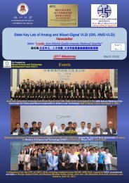
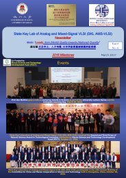
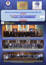
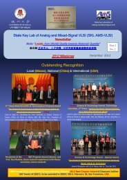
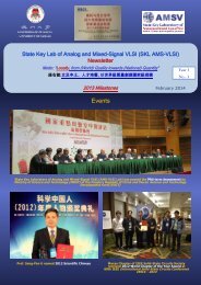
Events<br />
President Xi Jinping visited UM, and listened to the report of SKL (<strong>AMSV</strong>-VLSI) research achievements. President Xi<br />
mentioned that was happy to see the self-developed state-of-the-art leading chips and encouraged our team to contribute<br />
further to China high-level strategy policy of "Leading by Innovation" - as quoted by online Chinese Media.<br />
At Macao Science and Technology Awards presented this<br />
year, SKL AMS-VLSI won two 2nd and one 3rd prizes in<br />
the Technological Invention Award category. Also, Technology<br />
Development Award was granted to 3 PhD students<br />
and 1 Master Student from SKL AMS-VLSI<br />
SKL AMS-VLSI awarded "Excellence in INNOVATION"<br />
by Business Awards of Macau on Nov-<strong>2014</strong>
900MS/s 11b ADC (65nm)<br />
State-of-the-Art Chips - Designed and Tested in <strong>2014</strong> (9 chips)<br />
DCSP Chips<br />
Integrated Power Chips<br />
A 123-Phase DC-DC Converter-Ring with Fast-DVS for<br />
Microprocessors (65nm)<br />
430μm<br />
Ch.1<br />
Ch.2<br />
2 nd -stage<br />
1 st -stage<br />
340μm<br />
CLK Gen.<br />
Output Buffers<br />
Wireless Chips<br />
High efficient 5GHz ADC (65nm)<br />
A VCO-based Switched-Capacitor DC-DC Converter with Segment<br />
Frequency Modulation Control for Fast Recovery (65nm)<br />
BME (Biomedical Engineering) Chips<br />
Ultra-high Area Efficient and Low-<br />
Power Wireless Receiver (65nm)<br />
Single Chip Solar Energy<br />
Harvesting IC (180nm)<br />
Supply Modulated Micro-stimulator<br />
with Energy Recycling (180nm)<br />
ISSCC 2015<br />
µNMR Transceiver for Chemical/Biological Diagnosis and<br />
Ultra-low Power Wavelet Shrinkage ECG Processor (180nm)<br />
Optogenetic Frontend IC and Nested-<br />
Current-Mirror Amplifier (180nm)<br />
Four PhD students and one assistant professor from the University of Macau (UM) State Key Laboratory of Analog<br />
and Mixed-Signal VLSI (AMS-VLSI Lab) and Faculty of Science and Technology attended the Institute of Electrical<br />
and Electronics Engineer’s (IEEE) 62 nd International Solid-State Circuits Conference (ISSCC) in February 2015,<br />
which is considered the ‘Chip Olympics’, the most competitive conference in the field of chip design.<br />
The 6 papers from UM were "A 5.5mW 6b 5GS/s 4-times<br />
Interleaved 3b/cycle SAR ADC in 65nm CMOS", "A Multi-<br />
Step Multi-Sample µNMR Relaxometer Using Inside-Magnet<br />
Digital Microfluidics and a Butterfly-Coil-Input CMOS<br />
Transceiver", "A 12b 180MS/s 0.068mm 2 Full-Calibration-<br />
Integrated Pipelined-SAR ADC", "A 123-Phase DC-DC<br />
Converter-Ring with Fast-DVS for Microprocessors", "A<br />
0.028mm 2 11mW Single-Mixing Blocker-Tolerant Receiver<br />
with Double-RF N-Path Filtering, S 11 Centering, +13dBm<br />
OB-IIP 3 and 1.5-to-2.9dB NF", and "A 2-/3-Phase Fully-<br />
Integrated Switched-Capacitor DC-DC Converter in Bulk-<br />
CMOS for Energy-Efficient Digital Circuits With 14% Efficiency<br />
Improvement". There included 2 Pre-Doctoral<br />
Achievement Awards and 2 Student Research Previews.<br />
UM’s 1st book in<br />
Power Electronics<br />
UM PhD graduates to join the world’s No 1 mobile chip maker and Asia’s largest<br />
fabless IC design company<br />
Four PhD graduates from SKL AMS-VLSI recently<br />
passed their oral defenses, with external examiners<br />
unanimously praising their works for<br />
reaching world-class standards. The 4 new doctors<br />
are Un Ka-Fai, Yan Zushu, Lin Zhicheng,<br />
and Lin Fujian. Two of them have received job<br />
contracts from Qualcomm in the United States,<br />
which is the world’s No 1 mobile chip maker. One<br />
has joined Mediatek in Singapore, which is<br />
Asia’s largest fabless IC design company and<br />
ranks No 4 in the world. The last has decided to<br />
stay at UM as a post-doctoral researcher.<br />
US Patents granted in <strong>2014</strong><br />
1. C. Shi, M. K. Law and A. Bermak, “Method and Apparatus for Energy Harvesting using CMOS Sensor”, US<br />
Patent, US8629386 B2, Jan. 14, <strong>2014</strong>.<br />
2. Chi-Hang Chan, Yan Zhu, U-Fat Chio, Sai-Weng Sin, Seng-Pan U and Martins, R.P., "Comparator and<br />
Calibration Thereof", US Patent, US8829942 B2, Sept. 9, <strong>2014</strong>.
Selected works from each research line<br />
In ESSCIRC <strong>2014</strong><br />
An 11b 900 MS/s Time-Interleaved Sub-ranging Pipelined-SAR ADC<br />
[Best Paper Award]<br />
Yan Zhu, Chi-Hang Chan, Seng-Pan U, Rui P. Martins<br />
From Data Conversion and Signal Processing research line<br />
Motivation<br />
The highly Time-Interleaved(TI) SAR ADC with<br />
timing-calibration obtains the best power efficiency<br />
for the GHz speed goal, which removes<br />
the power and accuracy trade-off in the clock<br />
generator. However, the calibration sensitivity is<br />
limited by the type of input signal or the other<br />
non-idealities among sub-SAR ADCs such as<br />
reference noise, offset and gain mismatches.<br />
The skew calibration achieves better than 63dB<br />
SFDR in a TI-SAR ADC with GHz sampling rate<br />
and 10b resolution, while the calibration power<br />
from offset, gain and timing occupies near 50%<br />
total ADC power. This paper presents an 11b TI<br />
-sub-ranging pipelined-SAR ADC that achieves<br />
a maximum 1.1GS/s sampling rate with competitive<br />
power-efficiency as compared with the<br />
timing-calibrated TI-SAR ADCs. We propose the<br />
optimization Based on ADC’s sampling frontend<br />
for better SFDR by using the proposed<br />
channel-selection-embedded bootstrap rather<br />
than timing-calibration.<br />
Architecture<br />
Channel Selection Embedded (CSE)<br />
Bootstrap Circuit<br />
Φ 1(Φ 2)<br />
ΦM<br />
Φ1<br />
Vin<br />
Φ2<br />
Vdd<br />
2 Main S/H<br />
channels<br />
CSE<br />
Bootstrap<br />
A1<br />
CSE<br />
Bootstrap<br />
A2<br />
CF<br />
CF<br />
Vin<br />
6 Sub-S/H channels<br />
Φ1,1<br />
Φ1,2<br />
Φ1,3<br />
Φ2,1<br />
Φ2,2<br />
Φ2,3<br />
VB1(B2)<br />
DAC<br />
DAC<br />
DAC<br />
DAC<br />
DAC<br />
DAC<br />
Bootstraped<br />
switch<br />
M4<br />
A1(A2) M3<br />
V dd<br />
M1<br />
Φ P1(Φ P2)<br />
M2<br />
Φ s(Φ s)<br />
Φ M<br />
System Implementation<br />
Power (dB)<br />
System Implementation<br />
Gain Mismatches offset Mismatches<br />
0<br />
fs=900MS/s, fin=11MHz<br />
HD3<br />
HD2<br />
HD4<br />
HD5 HD8<br />
-100<br />
Verification<br />
Power (dB)<br />
0 0.1 0.2 0.3 0.4 0.5<br />
Normalized Frequency (fin / fs)(decimate by 25)<br />
Skew/Gain Mismatches offset Mismatches<br />
0<br />
SNR = 51.7 dB, SNDR = 51.5 dB, fs=900MS/s, fin=431MHz<br />
SFDR = 65.9 dB, THD = -64.3 dB<br />
HD3<br />
HD8 HD2<br />
-100<br />
0 0.1 0.2 0.3 0.4 0.5<br />
Normalized Frequency (fin / fs)(decimate by 25)<br />
SNDR & SFDR (dB)<br />
70<br />
68<br />
66<br />
64<br />
62<br />
60<br />
58<br />
56<br />
54<br />
52<br />
50<br />
SFDR<br />
SNR<br />
SNDR<br />
CLK Jitter 650fs<br />
10 100 200 300 400 500<br />
Input frequency (MHz) @f s=900MS/s<br />
Verification<br />
[1]<br />
[2]<br />
[3]<br />
[8]<br />
ISSCC’14 ISSCC’14 JSSCC’13 VLSI’13<br />
This Work<br />
Architecture<br />
Technology (nm)<br />
TI-SAR<br />
40<br />
TI-SAR<br />
65<br />
TI-SAR<br />
65<br />
Pipeline<br />
65<br />
TI-Pipelined-SAR<br />
65<br />
Resolution (bit)<br />
Sampling Rate (MS/s)<br />
Supply Voltage (V)<br />
10<br />
1.62<br />
1.1<br />
10<br />
1<br />
1<br />
10<br />
2.8<br />
1<br />
10<br />
0.8<br />
1.2<br />
11<br />
0.9<br />
1.2/1.2<br />
11<br />
1.1<br />
1.2/1.3<br />
Input Swing (Vp-p)<br />
1<br />
N/A N/A<br />
1.8 1.2 1.2<br />
SNDR @DC (dB)<br />
SNDR @Nyq. (dB)<br />
51<br />
48<br />
53.5<br />
51.2<br />
53.5<br />
51.2<br />
51<br />
48<br />
57.6<br />
51.5<br />
56.2<br />
50.7<br />
SFDR @Nyq. (dB) 62 60 55<br />
N/A 65.9 64<br />
DNL/INL (LSB)<br />
N/A 0.1/0.1 N/A 0.7/1.8 0.66/1.5 0.69/1.6<br />
Area (mm 2 )<br />
0.83<br />
0.78<br />
1.7<br />
0.18<br />
0.15<br />
Power (mW)<br />
71<br />
19.8<br />
44.6<br />
19 15.5 18<br />
FoM @DC (fJ/conv.step) 150<br />
51 56<br />
53 28 32<br />
FoM @Nyq. (fJ/conv.step) 210<br />
62 78<br />
71 56 58<br />
Require Timing Correction Yes Yes Yes No No<br />
Calibration (on-chip)<br />
Offset, gain,<br />
time<br />
Offset Offset, time No Offset
Normalized Power-delay product<br />
In TVLSI 2015<br />
Energy Optimized Sub-threshold VLSI Logic Family with Unbalanced<br />
Pull-up/down Network and Inverse-Narrow-Width Techniques<br />
Ming-Zhong Li, Chio-In Ieong, Man-Kay Law, Pui-In Mak, Mang-I Vai, Sio-Hang Pun and Rui P.<br />
Martins<br />
From Biomedical IC research line<br />
(Accepted in <strong>2014</strong>)<br />
Motivation<br />
Ultra-low-energy biomedical applications have<br />
urged the development of a sub-threshold VLSI<br />
logic family in standard CMOS. Instead of the<br />
traditionally preferred balanced pull-up (PU) and<br />
pull-down (PD) network approach in logic cell<br />
design, this work proposes an unbalanced pullup/down<br />
network together with an inversenarrow-width<br />
technique to improve the operating<br />
speed of the individual logic cell. Effective logical<br />
efforts save both power and die area in the process<br />
of device sizing and topology optimization.<br />
Three experimental 14-tap 8-bit finite impulse<br />
response (FIR) filters optimized for ultra-lowvoltage<br />
operation were fabricated in 0.18-μm<br />
CMOS. Measurements show that the optimized<br />
0.45-V and 0.6-V libraries achieve minimum energy<br />
operations at 100 kHz, with a Figure-of-<br />
Merit (FoM) of 0.365 (at 0.31 V) and 0.4632 (at<br />
0.39 V), respectively. They correspond to<br />
35.96% and 18.74% improvements, and the<br />
overall performances are well comparable with<br />
the state-of-the-art.<br />
Power-delay product (J)<br />
10 -17<br />
10 -18<br />
10 -19<br />
Architecture<br />
10 -15 Operating<br />
with balancing<br />
w/o balancing<br />
frequency limit<br />
10 -16 difference<br />
(unbalanced)<br />
40%<br />
30%<br />
20%<br />
10%<br />
0%<br />
10 3 10 4 10 5 10 6<br />
Frequency (Hz)<br />
10 7<br />
Difference in power-delay product<br />
4.0<br />
3.2<br />
2.4<br />
1.6<br />
WNMOS = 0.88 mm<br />
WNMOS = 0.66 mm<br />
WNMOS = 0.44 mm<br />
WNMOS = 0.22 mm<br />
0.8<br />
0.2 0.4 0.6 0.8 1 1.2 1.4<br />
PMOS Width (mm)<br />
Power-delay product of an inverter (FO4 loading) with balanced (P/N ratio =<br />
5/1) and unbalanced (P/N ratio = 2/1) PU/PD network vs. operating frequency<br />
at 0.3 V (left); Normalized power-delay product of a FO4 inverter at various<br />
NMOS/PMOS widths at 0.3 V (right).<br />
0.5<br />
NMOS VT (V)<br />
Minimum<br />
PMOS |VT|<br />
-0.41<br />
PMOS VT (V)<br />
0.5<br />
Minimum PMOS<br />
|VT| interval @<br />
400 – 590 nm<br />
-0.46<br />
Minimum<br />
Minimum<br />
NMOS VT<br />
NMOS VT<br />
@ 220 nm<br />
0.42<br />
-0.49 0.42<br />
-0.5<br />
0 0.5 1 1.5 2 2.5<br />
0.1 0.5 0.9 1.3 1.7 2.1 2.5<br />
Transistor Length (mm)<br />
Transistor Width (mm)<br />
NMOS/PMOS VT vs. transistor length (left); Transistor width (right)<br />
at VDD = 0.3 V.<br />
NMOS VT (V)<br />
INW<br />
PMOS VT (V)<br />
System Implementation<br />
Verification<br />
Normalized Energy/Cycle<br />
1.0<br />
0.6<br />
0.2<br />
Circuit with 0.30-V .lib<br />
Circuit with 0.45-V .lib<br />
Circuit with 0.60-V .lib<br />
0.32V<br />
0.44V<br />
0.34V<br />
0<br />
0.25 0.35 0.45 0.55<br />
Power Supply Voltage (V)<br />
Normalized Energy/Cycle<br />
Circuit with 0.30-V .lib<br />
Circuit with 0.45-V .lib<br />
1.0<br />
Circuit with 0.60-V .lib<br />
0.6<br />
0.28V<br />
0.39V<br />
0.2 0.31V<br />
0<br />
0.25 0.35 0.45 0.55<br />
Power Supply Voltage (V)<br />
0.35 mm<br />
0.3 V liberty<br />
file (.lib)<br />
based FIR<br />
0.33 mm<br />
0.2 mm<br />
0.265 mm<br />
0.45 V liberty<br />
file (.lib)<br />
based FIR<br />
0.25 mm<br />
0.196 mm<br />
0.6 V liberty<br />
file (.lib)<br />
based FIR<br />
Die micrographs of the 0.18-µm sub-threshold FIR test chips using the 0.3V,<br />
0.45V and 0.6V liberty file.<br />
Die micrographs of the 0.18-µm sub-threshold FIR test chips using the 0.3V,<br />
0.45V and 0.6V liberty file.<br />
Number of Chips<br />
5<br />
4<br />
3<br />
2<br />
1<br />
σ = 0.0678 pJ<br />
μ = 0.3829 pJ<br />
0<br />
0 0.33 0.37 0.41 0.45 0.49 0.53 0.60<br />
Energy/Cycle (pJ)<br />
Number of Chips<br />
4<br />
3<br />
2<br />
1<br />
σ = 0.0543 pJ<br />
μ = 0.4995 pJ<br />
0<br />
0 0.41 0.45 0.49 0.53 0.57 0.63<br />
Energy/Cycle (pJ)<br />
Die micrographs of the 0.18-µm sub-threshold FIR test chips using the 0.3V,<br />
0.45V and 0.6V liberty file.
Voltage<br />
Voltage<br />
In American Institute of Physics – Advances <strong>2014</strong><br />
Natural Discharge after Pulse and Cooperative Electrodes to<br />
Enhance Droplet Velocity in Digital Microfluidics<br />
Tianlan Chen, Cheng Dong, Jie Gao, Yanwei Jia, Pui-In Mak, Mang-I Vai, and Rui P. Martins<br />
From Multidisciplinary Research Area<br />
Motivation<br />
Architecture<br />
Digital Microfluidics (DMF) is a promising technology<br />
for biological/chemical micro-reactions<br />
due to its distinct droplet manageability via electronic<br />
automation, but the limited velocity of<br />
droplet transportation has hindered DMF from<br />
utilization in high throughput applications.<br />
In this paper, by adaptively fitting the actuation<br />
voltages to the dynamic motions of droplet<br />
movement under real-time feedback monitoring,<br />
two control-engaged electrode-driving techniques:<br />
Natural Discharge after Pulse (NDAP)<br />
and Cooperative Electrodes (CE) are proposed.<br />
They together lead to, for the first time, enhanced<br />
droplet velocity with lower root mean<br />
square voltage value.<br />
uα<br />
uβ<br />
uβ’<br />
0<br />
uα<br />
uβ<br />
uβ’<br />
0<br />
HV period<br />
tα’<br />
LV period<br />
tβ<br />
tα<br />
1 st electrode<br />
tthc<br />
tths<br />
tths<br />
Time<br />
NDAP<br />
2 nd electrode<br />
NDAP + CE<br />
(a)<br />
(b)<br />
uα<br />
0<br />
uα<br />
0<br />
Sketches of four possible electrode-driving schemes for droplet movements<br />
over two electrodes: (a) Natural Discharge after Pulse (NDAP): The highvoltage<br />
(HV) period lasts shorter, while the low-voltage (LV) under natural<br />
discharge lasts longer with short pulse recharging periodically. (b) DC signal.<br />
(c) NDAP with cooperative electrodes (CE) overlaps the charging time of<br />
neighboring electrodes. (d) DC plus CE driving. (e) Droplet moving toward<br />
two target electrodes and location of the two thresholds on the first target<br />
electrode. The electrode was grounded when the charging was done in all<br />
schemes.<br />
tthc<br />
tths<br />
tths<br />
Time<br />
DC<br />
DC + CE<br />
(c)<br />
(d)<br />
thc<br />
ths<br />
1st<br />
2nd<br />
(e)<br />
Result I<br />
Result II<br />
(a) Velocity comparison of NDAP signals with different and DC. NDAP with<br />
13-ms to 100-ms has average velocities higher than DC signal. (b) Video<br />
frames of a droplet actuated by NDAP and DC crossing 2 electrodes<br />
(Multimedia view). Video was captured by a high speed camera (Nikon V2),<br />
which has a maximum frame rate up to 1200 frames/second (resolution 320<br />
x 120 pixels). A LED light was set in the same frame to light on when the<br />
electrode was being charged. Individual frames extracted from the videos<br />
were analyzed by the image processing software Image J to obtain the<br />
v droplet.<br />
Comparison between the proposed (NDAP + CE and high-speed feedback)<br />
and classical (DC) schemes for droplet movements in a long run of 3 s: (a)<br />
Droplet successfully moved across 12 electrodes when it was controlled by<br />
the proposed scheme. The path of the droplet’s center had been shortened<br />
at electrode No. 6 by CE, which charged electrode No. 7 before the droplet<br />
reached electrode No. 6, resulting in an upward move of droplet in advance.<br />
The whole droplet transportation was recorded in video (Multimedia view).<br />
(b) Droplet failed to complete movement in 3 s due to its lower speed. The<br />
moving path was close to the right angle at the two corners. The whole<br />
droplet transportation was recorded in video (Multimedia view). (c) Instantaneous<br />
velocity of the droplet moving across the electrodes. As expected,<br />
droplet controlled by the proposed scheme moved across electrode No. 6-7-<br />
8 using a much shorter time than that of the classical procedure.
In Royal Society of Chemistry - Analyst <strong>2014</strong><br />
NMR-DMF: A Modular Nuclear Magnetic Resonance–Digital<br />
Microfluidics System for Biological Assays<br />
Ka-Meng Lei, Pui-In Mak, Man-Kay Law, and Rui P. Martins<br />
From Multidisciplinary Research Area<br />
Motivation<br />
Architecture I<br />
We present a modular nuclear magnetic resonance–digital<br />
microfluidics (NMR-DMF) system<br />
as a portable diagnostic platform for miniaturized<br />
biological assays.<br />
With increasing numbers of combination between<br />
designed probes and a specific target,<br />
NMR becomes an accurate and rapid assay tool<br />
capable of detecting particular kinds of proteins,<br />
DNAs, bacteria and cells with a customized<br />
probe quantitatively.<br />
Traditional sample operation (e.g., manipulation<br />
and mixing) relied heavily on human efforts. We<br />
herein propose a modular NMR-DMF system to<br />
allow electronic automation of multi-step reaction-screening<br />
protocols.<br />
The overall schematics and operations of the NMR-DMF system. (a) The<br />
placement of the DMF chip, magnet, RF coil and PCB board in 3D view. Benefit<br />
from the plane-parallel magnetic field generated by the figure-8 shaped coil,<br />
the NMR system can be effectively integrated into the DMF system; (b) Schematics<br />
of the NMR Electronics. The transmitter which is formed by the digital<br />
logics such as flip flops is used to excite the hydrogen atom. On the receiver<br />
part, the capacitor together with the RF-coil (fabricated figure-8 shaped coil)<br />
forms a LC tank to provide passive gain enhancing of the system’s sensitivity.<br />
The signal is then amplified and down converted to f IF (intermediate frequency)<br />
and fed to the external filters and oscilloscope; (c) The filtered results from the<br />
PCB are captured by the oscilloscope for easier demonstration purpose.<br />
Waveforms are then analysed and the spin-spin relaxation time (T 2) is fitted by<br />
the algorithm written in MATLAB; (d) The photograph of the DMF chip and<br />
structure of the DMF platform. The droplets are squeezed between the top and<br />
bottom planes and surrounded by silicone oil; (e) The detection mechanism of<br />
the NMR-DMF system. The target-specific magnetic nanoparticles, which act<br />
as probes, are placed on the sensing site initially (in purple). The samples at<br />
other electrodes (in cyan) will be transported to the sensing site and mixed with<br />
the probes to perform NMR assays automatically by applying voltage on corresponding<br />
electrodes. Without the target, the probes stay monodispersed and<br />
will have a longer T 2. Otherwise, the target and probes will form clusters by<br />
forming bonds between each other and the T 2 will be decreased.<br />
Architecture II<br />
Result<br />
(a) Plot of unit magnetic field in y-direction of the 14-turn figure-8 shaped coil<br />
along z-axis. The magnetic field is stronger on the coil surface (1.8 mT) and<br />
starts to decrease above the coil. Inset shows the photograph of the 14-turn<br />
figure-8 shaped coil; (b) The magnetic flux lines of the simulated 14-turn<br />
figure-8 shaped coil. The magnetic fluxes are still pointing in the z-direction<br />
at the centres of each coil. However, between the two coils, the magnetic<br />
flux is pointing in the y-direction, generating plane-parallel magnetic flux. (c)<br />
Plane-parallel magnetic flux density map of the 14-turn figure-8 shaped coil<br />
at z = 0.6 mm (depth of the ITO glass). The sensing region, which is defined<br />
as the area have a plane-parallel magnetic flux density larger than 50% its<br />
peak value (1.43 mT) is located between the centers of two coils and has a<br />
shape of circle with diameter around 4.2 mm.<br />
(a) Illustration of droplets mixing. The droplets at electrode no. 1 (samples)<br />
and no. 8 (probe) were driven to electrode no.7 and mixed together. (b) The<br />
NMR assay results from the mixed droplets. Biotinylated magnetic nanoparticles<br />
acted as a probe. If the samples do not contain avidin, the nanoparticles<br />
will stay monodispersed and a longer T 2 will be obtained (181.5 ms). If<br />
avidin is with the samples, avidin and biotin will combine to form rigid bond<br />
and clusters will be presented. In consequence, T 2 will be decreased by the<br />
perturbation of the magnetic nanoparticle clusters (86.13 ms). This shows<br />
that the system is capable of detecting the existence of protein in the samples<br />
in a fully-automated way.
In ISSCC <strong>2014</strong> and JSSC <strong>2014</strong><br />
A 0.5V 1.15mW 0.2mm 2 Sub-GHz ZigBee Receiver Supporting<br />
433/860/915/960MHz ISM Bands with Zero External Components<br />
[ISSCC <strong>2014</strong> Highlight]<br />
Zhicheng Lin, Pui-In Mak and Rui P. Martins<br />
From Wireless IC research line<br />
Motivation<br />
Architecture<br />
The rapid proliferation of Internet of Things<br />
has urged the development of ultra-low-power<br />
(ULP) radios at the lowest possible cost, while<br />
being universal for worldwide markets.<br />
This work is a single-0.5V ULP receiver for<br />
sub-GHz ZigBee (IEEE 802.15.4c/d) products.<br />
With 1.15mW of power and 0.2mm 2 of area,<br />
the receiver shows 8.1-dB NF and –20.5dBm<br />
IIP 3 over the 433/860/915/960MHz ISM bands<br />
apt for China, Europe, North America and Japan,<br />
respectively, with zero external component.<br />
System Implementation<br />
Verification
A 123-Phase DC-DC Converter-Ring with Fast-DVS for<br />
Microprocessors<br />
Yan Lu, Junmin Jiang, Wing-Hung Ki, C. Patrick Yue, Sai-Weng Sin, Seng-Pan U, and Rui P.<br />
Martins<br />
From Integrated Power research line<br />
In ISSCC 2015<br />
(Accepted in <strong>2014</strong>)<br />
Motivation<br />
Inspired by The Square of Vatican City, a fully-integrated<br />
step-down switched-capacitor DC-DC converter-ring with<br />
100+ phases is designed with a fast-DVS (dynamic voltage<br />
scaling) feature for the microprocessor in portable/<br />
wearable devices.<br />
Switched-capacitor power converters (SCPCs) are preferred<br />
for full integration because the capacitor density<br />
has increased significantly in nm processes. Multiphase<br />
architecture for ripple reduction can be easily built into the<br />
SCPC with little power and area overheads.<br />
This symmetrical ring-shaped converter surrounds its load<br />
in the square and supplies the on-chip power grid, such<br />
that a good quality power supply can be easily accessed<br />
at any point of the chip edges. There are 30 phases on<br />
the top edge and 31 phases on each of the other 3 edges,<br />
making 123 phases in total. The phase number and unit<br />
cell dimensions of this architecture can easily be modified<br />
to fit the floor plan of the load.<br />
By using the proposed VDD-controlled oscillator (V DD CO)<br />
the frequency of which is controlled by varying its supply<br />
voltage, a hitherto unexplored feature of the multiphase<br />
DC-DC architecture is exposed: the control-loop unity<br />
gain frequency (UGF) could be designed to be higher<br />
than the switching frequency.<br />
Architecture<br />
For the conventional PFM topology that uses a centralized<br />
current-starved (CS) voltage-controlled oscillator (VCO) and<br />
distributed clock phases, the upper limit on phase number is<br />
due to the matching of phases and routings; and its dominant<br />
pole is usually set at the VCTL node.<br />
For the proposed topology, the error amplifier (EA) with<br />
NMOS source follower buffer stage drives the VDDCO which<br />
is distributed and localized to every phase that makes it free<br />
of matching and routing problems. Now, VDDC is a lowimpedance<br />
node and the associated pole is located at high<br />
frequencies; and the output pole becomes the dominant pole<br />
and the bandwidth is extended.<br />
System Implementation<br />
Verification
Events and Visits<br />
Visit by Mr. Ma Chi Ngai Frederico, President of FDCT<br />
Visit by Prof. Bai Chun Li, President of Chinese<br />
Academy of Sciences<br />
Distinguished Lectures on Microelectronics and Biomedical Engineering<br />
IEEE Solid-State Circuits Society <strong>2014</strong> Distinguished Lecture Workshop -<br />
Macau by Prof. Jan Van der Spiegel, University of Pennsylvania, Prof. Tzi<br />
-Dar Chiueh, National Taiwan University, Prof. Howard Luong, HKUST<br />
2-Day Workshop on Integrated Power and Energy in Semiconductor<br />
by Prof. LEO LORENZ, IEEE Fellow, Member of German National Academy<br />
of Sciences, President of European Center of Power Electronics (ECPE)<br />
A/D Converter Circuit and Architecture Design for High-speed<br />
Data Communication by<br />
Prof. Boris MURMANN, Stanford University, USA<br />
Biosensors - Playing at the Crossroads of Engineering and the Sciences<br />
by<br />
Dr. M. Jamal Deen FRSC, McMaster University, Canada<br />
Two New Academics Joined SKL AMS-VLSI<br />
Dr. Jun Yin received the B.Sc. and the M.Sc. degrees in Microelectronics from Peking University, Beijing, China, in 2004 and 2007,<br />
respectively, and the Ph.D. degree in Electronic and Computer Engineering (ECE) from Hong Kong University of Science and Technology<br />
(HKUST), Hong Kong, China, in 2013.<br />
Research Interests: CMOS RF and mm-Wave integrated circuits for wireless communication and wireless sensing systems.<br />
Dr. Yan Lu received the B.Eng. and M.Sc. degrees in Microelectronic Engineering from South China University of Technology, Guangzhou,<br />
China, in 2006 and 2009, respectively; and the Ph.D. degree in Electronic and Computer Engineering from the Hong Kong University<br />
of Science and Technology, Hong Kong, China, in 2013. He was a Visiting Scholar at University of Twente, the Netherlands, in<br />
2013 for four months.<br />
Research interests: Wireless power transfer systems, fully-integrated DC-DC converters, low-dropout regulators and RF energy harvesting.
SCI Journals – 20 Papers<br />
▓ Hugo Horta, R. P. Martins, "The start-up, evolution and impact of a research group in a university developing its knowledge base",<br />
Tertiary Education and Management, Taylor & Francis, vol. 20, No.4, pp. 280-293, Dec. <strong>2014</strong><br />
▓ Zhicheng Lin, Pui-In Mak, R. P. Martins, "A Sub-GHz Multi-ISM-Band ZigBee Receiver Using Function-Reuse and Gain-Boosted N-Path<br />
Techniques for IoT Applications", IEEE Journal of Solid-State Circuits, vol. 49, Issue 12, pp. 2990 - 3004, Dec. <strong>2014</strong><br />
▓ Fujian Lin, Pui-In Mak, R. P. Martins, "An RF-to-BB-Current-Reuse Wideband Receiver with Parallel N-Path Active/Passive Mixers and a<br />
Single-MOS Pole-Zero LPF", IEEE Journal of Solid-State Circuits, vol. 49, Nov. <strong>2014</strong><br />
▓ D. G. Chen, F. Tang, M. K. Law, X. Zhong and A. Bermak, "A 64-fJ/step 9-bit SAR ADC Array with Forward Error Correction and mixed<br />
-signal CDS for CMOS Image Sensors," IEEE Transactions on Circuits and Systems-I, vol. 61, issue 11, pp. 3085-3093, Nov.<br />
<strong>2014</strong><br />
▓ Md.Tawfiq Amin, Pui-In Mak and R. P. Martins, "A 0.137-mm 2 9-GHz Hybrid Class-B/C QVCO with Output Buffering in 65-nm CMOS,"<br />
IEEE Microwave and Wireless Components Letters, vol. 24, pp. 716-718, Oct. <strong>2014</strong><br />
▓ Zhicheng Lin, Pui-In Mak, R. P. Martins, "Analysis and Modeling of a Gain-Boosted N-Path Switched-Capacitor Bandpass Filter", IEEE<br />
Transactions on Circuits and Systems – I, vol. 9, pp. 2560-2568, Sept. <strong>2014</strong><br />
▓ NingYi Dai, Chi-Seng Lam, WenChen Zhang, “Multifunctional voltage source inverter for renewable energy integration and power<br />
quality conditioning”, The Scientific World Journal, vol. <strong>2014</strong>, Aug. <strong>2014</strong><br />
▓ K. M. Lei, P. I. Mak, M. K. Law and R. P. Martins, “NMR-DMF: A Modular Nuclear Magnetic Resonance-Digital Microfluidics System for<br />
Biological Assays,” RSC Analyst, <strong>2014</strong>, 139, 6204-6213, Aug. <strong>2014</strong><br />
▓ Zhicheng Lin, Pui-In Mak, R. P. Martins, "A 0.14-mm 2 , 1.4-mW, 59.4 dB-SFDR, 2.4-GHz ZigBee/WPAN Receiver Exploiting a Split-LNTA<br />
+ 50% LO Topology in 65-nm CMOS", IEEE Transactions on Microwave Theory and Techniques, vol. 62, pp. 1525-1534 , Jul.<br />
<strong>2014</strong><br />
▓ Zhicheng Lin, Pui-In Mak, R. P. Martins, "A 2.4-GHz ZigBee Receiver Exploiting an RF-to-BB-Current-Reuse Blixer + Hybrid Filter<br />
Topology in 65-nm CMOS", IEEE Journal of Solid-State Circuits, vol. 49, pp. 1333-1344, Jun. <strong>2014</strong><br />
▓ Pui-In Mak, Miao Liu, Yaohua Zhao, R. P. Martins, "Enhancing the Performances of Recycling Folded Cascode OpAmp in Nanoscale<br />
CMOS through Voltage Supply Doubling and Design for Reliability", Wiley International Journal of Circuit Theory and Applications,<br />
vol. 42, pp. 605-619, Jun. <strong>2014</strong><br />
▓ Yan Lu, Wing-Hung Ki, “A 13.56 MHz CMOS Active Rectifier with Switched-Offset and Compensated Biasing for Biomedical Wireless<br />
Power Transfer Systems”, IEEE Transactions on Biomedical Circuits and Systems, vol. 8, pp.334-344, Jun. <strong>2014</strong><br />
▓ C. H. Chen, S. H. Pun, P. U. Mak, M. I. Vai, A. Klug, et al., "Circuit Models and Experimental Noise Measurements of Micropipette<br />
Amplifiers for Extracellular Neural Recordings from Live Animals," BioMed Research International, vol. <strong>2014</strong>, p. 14, Jun. <strong>2014</strong><br />
▓ Chi-Seng Lam, Man-Chung Wong, Wai-Hei Choi, Xiao-Xi Cui, Hong-Ming Mei, Jian-Zheng Liu, “Design and Performance of an adaptive<br />
low dc voltage controlled LC-hybrid active power filter with a neutral inductor in three-phase four-wire power systems”, IEEE<br />
Transactions on Industrial Electronics, vol. 61, no. 6, pp. 2635-2647, Jun. <strong>2014</strong><br />
▓ D. G. Chen, F. Tang, M. K. Law and A. Bermak, “A 12 pJ/pixel Analog-to-Information Converter based 816 x 640 Pixel CMOS Image<br />
Sensor”, IEEE Journal of Solid-State Circuits, vol. 49, issue 5, pp. 1210-1222, May <strong>2014</strong><br />
▓ Ning-Yi Dai, Man-Chung Wong, Keng-Weng Lao, Chi-Kong Wong, “Modelling and control of a railway power conditioner in co-phase<br />
traction power system under partial compensation”, IET Power Electronics, vol. 7, no. 5, pp. 1044 - 1054, May <strong>2014</strong><br />
▓ Tianlan Chen, Cheng Dong, Jie Gao, Yanwei Jia, Pui-In Mak, Mang-I Vai and R. P. Martins, “Natural Discharge after Pulse and Cooperative<br />
Electrodes to Enhance Droplet Velocity in Digital Microfluidics,” AIP Advances, Apr. <strong>2014</strong><br />
▓ Fujian Lin, Pui-In Mak, R. P. Martins, "A Sine-LO Square-Law Harmonic-Rejection Mixer – Theory, Implementation and Application",<br />
IEEE Transactions on Microwave Theory and Techniques, vol. 62, pp. 313-322, Feb. <strong>2014</strong><br />
▓ B. Wang, M. K. Law, A. Bermak and H. C. Luong, “A Passive RFID Tag Embedded Temperature Sensor With Improved Process Spreads<br />
Immunity for a -30 o C to 60 o C Sensing Range”, IEEE Transactions on Circuits and Systems I, pp. 337 – 346, Feb. <strong>2014</strong><br />
▓ Yan Zhu, Chi-Hang Chan, U-Fat Chio, Sai-Weng Sin, Seng-Pan U, R.P. Martins, F. Maloberti, "Split-SAR ADCs: Improved Linearity With<br />
Power and Speed Optimization," IEEE Transactions on Very Large Scale Integration Systems, vol.22, no.2, pp.372,383, Feb.<br />
<strong>2014</strong><br />
Conferences – 23 Papers<br />
Major solid-state circuits conferences<br />
International Solid-State Circuits Conference (ISSCC) <strong>2014</strong>, San Francisco, CA, USA, Feb. <strong>2014</strong><br />
▓ “A 0.0013mm 2 3.6µW Nested-Current-Mirror Single-Stage Amplifier Driving 0.15-to-15nF Capacitive Loads with >62° Phase Margin”<br />
[Pre-Doctoral Achievement Award]<br />
▓ "An RF-to-BB current-reuse wideband receiver with parallel N-path active/passive mixers and a single-MOS pole-zero LPF"<br />
▓ "A 0.5V 1.15mW 0.2mm 2 Sub-GHz ZigBee receiver supporting 433/860/915/960MHz ISM bands with zero external components"<br />
▓ "Circuit Techniques for Switched-Capacitor Filters" [Student Research Preview]<br />
European Solid-State Circuits Conference (ESSCIRC) <strong>2014</strong>, Venice, Italy, Sept. <strong>2014</strong><br />
▓ “An 11b 900 MS/s time-interleaved sub-ranging pipelined-SAR ADC” [Best Paper Award]<br />
Other conferences:<br />
APPEEC <strong>2014</strong>, Hong Kong, China, Dec. <strong>2014</strong><br />
▓ “An adaptive hysteresis band PWM control for hybrid active power filters in fixed frequency”<br />
ISIC <strong>2014</strong>, Singapore, Dec. <strong>2014</strong><br />
▓ “A 0.3-V 37.5-nW 1.5~6.5-Input-Range Supply Voltage Tolerant Capacitive Sensor Readout”<br />
BMEiCON <strong>2014</strong>, Fukuoka, Japan, Nov. <strong>2014</strong><br />
▓ “Investigation on Error Performance for Galvanic-type Intra-body Communication with Experiment”<br />
APCCAS <strong>2014</strong>, Okinawa, Japan, Nov. <strong>2014</strong><br />
▓ “A Low-Dropout Regulator with Power Supply Rejection Improvement by Bandwidth-Zero Tracking”<br />
▓ “Analysis of Two-Phase on-Chip Step-Down Switched Capacitor Power Converter”<br />
▓ “Co-Design of a Low-Noise Receiver Front-End and its Exciting-Sensing Coil for Portable NMR-Screening of Chemical/Biological Droplets”<br />
▓ “A 104μW EMI-Resisting Bandgap Voltage Reference Achieving –20dB PSRR, and 5% DC Shift under a 4dBm EMI Level”<br />
Lab-on-a-Chip Asia <strong>2014</strong>, Singapore, Nov. <strong>2014</strong><br />
▓ “Time-Regulated Actuation Signal for Enhancement of Droplet Transportation in Digital Microfluidics”<br />
▓ “Electrical Actuation on Digital Microfluidics with a Ta2O5 Insulating Layer: a Comparison Study”<br />
GCBME <strong>2014</strong> & APCMBE <strong>2014</strong>, Tainan, Taiwan, Oct. <strong>2014</strong><br />
▓ “Initial Design of the Capacitive Micromachined Ultrasonic Transducers (CMUT) with Helmholtz Resonance Aperture”<br />
ECCE <strong>2014</strong>, Pittsburgh, PA, USA, Sept. <strong>2014</strong><br />
▓ “Hybrid railway power conditioner with partial compensation for rating optimization”<br />
IC-TEMS <strong>2014</strong>, ZhuHai, GuangDong, China, Jul. <strong>2014</strong><br />
▓ “The Fabrication and Application of a Robust and Intelligent Digital Microfluidics”<br />
ICIEA <strong>2014</strong>, Hangzhou, China, Jun. <strong>2014</strong><br />
▓ “Modeling of novel single flow zinc-nickel battery for energy storage system”<br />
ISCAS <strong>2014</strong>, Melbourne, Australia, Jun. <strong>2014</strong><br />
▓ “A High Voltage Zero-Static Current Voltage Scaling ADC Interface Circuit for Micro-Stimulator”<br />
▓ “Micropower Two-Stage Amplifier Employing Recycling Current-Buffer Miller Compensation”<br />
EDSSC <strong>2014</strong>, Chengdu, China, Jun. <strong>2014</strong><br />
▓ “A 26.3 dBm 2.5 to 6 GHz Wideband Class-D Switched-Capacitor Power Amplifier with 40% Peak PAE ”<br />
ICBME 2013, Singapore, Dec. 2013<br />
▓ “Effect of Transmitter and Receiver Electrodes Configurations on the Capacitive Intrabody Communication Channel from 100 kHz to 100 MHz”<br />
▓ ”Channel Modeling and Simulation for Galvanic Coupling Intra-body Communication”<br />
State Key Laboratory of Analog and Mixed-Signal VLSI / UM<br />
http://www.amsv.umac.mo