Data Sheet - Hobby Engineering
Data Sheet - Hobby Engineering
Data Sheet - Hobby Engineering

You also want an ePaper? Increase the reach of your titles
YUMPU automatically turns print PDFs into web optimized ePapers that Google loves.
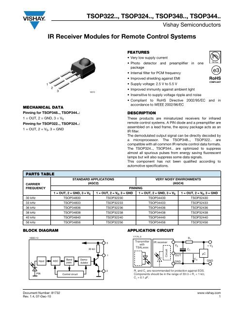
TSOP322.., TSOP324.., TSOP348.., TSOP344..<br />
Vishay Semiconductors<br />
IR Receiver Modules for Remote Control Systems<br />
MECHANICAL DATA<br />
1<br />
2<br />
Pinning for TSOP348.., TSOP344..:<br />
1 = OUT, 2 = GND, 3 = V S<br />
Pinning for TSOP322.., TSOP324..:<br />
1 = OUT, 2 = V S , 3 = GND<br />
3<br />
16672<br />
FEATURES<br />
• Very low supply current<br />
• Photo detector and preamplifier in one<br />
package<br />
• Internal filter for PCM frequency<br />
• Improved shielding against EMI<br />
• Supply voltage: 2.5 V to 5.5 V<br />
• Improved immunity against ambient light<br />
• Insensitive to supply voltage ripple and noise<br />
• Compliant to RoHS Directive 2002/95/EC and in<br />
accordance to WEEE 2002/96/EC<br />
DESCRIPTION<br />
These products are miniaturized receivers for infrared<br />
remote control systems. A PIN diode and a preamplifier are<br />
assembled on a lead frame, the epoxy package acts as an<br />
IR filter.<br />
The demodulated output signal can be directly decoded by<br />
a microprocessor. The TSOP348.., TSOP322.. are<br />
compatible with all common IR remote control data formats.<br />
The TSOP324.., TSOP344.. are optimized to suppress<br />
almost all spurious pulses from energy saving fluorescent<br />
lamps but will also suppress some data signals.<br />
This component has not been qualified according to<br />
automotive specifications.<br />
PARTS TABLE<br />
CARRIER<br />
FREQUENCY<br />
STANDARD APPLICATIONS<br />
(AGC2)<br />
VERY NOISY ENVIRONMENTS<br />
(AGC4)<br />
PINNING<br />
1 = OUT, 2 = GND, 3 = V S 1 = OUT, 2 = V S , 3 = GND 1 = OUT, 2 = GND, 3 = V S 1 = OUT, 2 = V S , 3 = GND<br />
30 kHz TSOP34830 TSOP32230 TSOP34430 TSOP32430<br />
33 kHz TSOP34833 TSOP32233 TSOP34433 TSOP32433<br />
36 kHz TSOP34836 TSOP32236 TSOP34436 TSOP32436<br />
38 kHz TSOP34838 TSOP32238 TSOP34438 TSOP32438<br />
40 kHz TSOP34840 TSOP32240 TSOP34440 TSOP32440<br />
56 kHz TSOP34856 TSOP32256 TSOP34456 TSOP32456<br />
BLOCK DIAGRAM<br />
APPLICATION CIRCUIT<br />
16833-13<br />
Input<br />
AGC<br />
Demo-<br />
dulator<br />
Band<br />
pass<br />
30 kΩ<br />
3<br />
1<br />
17170_5<br />
Transmitter<br />
with<br />
TSALxxxx<br />
IR receiver<br />
Circuit<br />
V S<br />
OUT<br />
GND<br />
R 1<br />
C 1<br />
V O<br />
µC<br />
+ V S<br />
GND<br />
PIN<br />
Control circuit<br />
2<br />
R 1<br />
and C 1<br />
are recommended for protection against EOS.<br />
Components should be in the range of 33 Ω < R 1<br />
< 1 kΩ,<br />
C 1<br />
> 0.1 µF.<br />
Document Number: 81732 www.vishay.com<br />
Rev. 1.4, 07-Dec-10 1
TSOP322.., TSOP324.., TSOP348.., TSOP344..<br />
Vishay Semiconductors<br />
IR Receiver Modules for Remote<br />
Control Systems<br />
ABSOLUTE MAXIMUM RATINGS<br />
PARAMETER TEST CONDITION SYMBOL VALUE UNIT<br />
Supply voltage V S - 0.3 to + 6 V<br />
Supply current I S 3 mA<br />
Output voltage V O - 0.3 to (V S + 0.3) V<br />
Output current I O 5 mA<br />
Junction temperature T j 100 °C<br />
Storage temperature range T stg - 25 to + 85 °C<br />
Operating temperature range T amb - 25 to + 85 °C<br />
Power consumption T amb ≤ 85 °C P tot 10 mW<br />
Soldering temperature t ≤ 10 s, 1 mm from case T sd 260 °C<br />
Note<br />
• Stresses beyond those listed under “Absolute Maximum Ratings” may cause permanent damage to the device. This is a stress rating only<br />
and functional operation of the device at these or any other conditions beyond those indicated in the operational sections of this specification<br />
is not implied. Exposure to absolute maximum rating conditions for extended periods may affect the device reliability.<br />
ELECTRICAL AND OPTICAL CHARACTERISTICS (T amb = 25 °C, unless otherwise specified)<br />
PARAMETER TEST CONDITION SYMBOL MIN. TYP. MAX. UNIT<br />
E v = 0, V S = 3.3 V I SD 0.27 0.35 0.45 mA<br />
Supply current<br />
E v = 40 klx, sunlight I SH 0.45 mA<br />
Supply voltage V S 2.5 5.5 V<br />
Transmission distance<br />
Output voltage low<br />
Minimum irradiance<br />
Maximum irradiance<br />
Directivity<br />
E v = 0, test signal see fig. 1,<br />
IR diode TSAL6200,<br />
I F = 250 mA<br />
I OSL = 0.5 mA, E e = 0.7 mW/m 2 ,<br />
test signal see fig. 1<br />
Pulse width tolerance:<br />
t pi - 5/f 0 < t po < t pi + 6/f 0 ,<br />
test signal see fig. 1<br />
t pi - 5/f 0 < t po < t pi + 6/f 0 ,<br />
test signal see fig. 1<br />
Angle of half transmission<br />
distance<br />
d 45 m<br />
V OSL 100 mV<br />
E e min. 0.1 0.25 mW/m 2<br />
E e max. 30 W/m 2<br />
ϕ 1/2 ± 45 deg<br />
TYPICAL CHARACTERISTICS (T amb = 25 °C, unless otherwise specified)<br />
E e Optical Test Signal<br />
(IR diode TSAL6200, I F = 0.4 A, 30 pulses, f = f 0 , t = 10 ms)<br />
1<br />
0.9<br />
Output Pulse Width<br />
0.8<br />
t<br />
0.7<br />
Input Burst Length<br />
t pi *<br />
0.6<br />
T<br />
0.5<br />
* t pi 10/f 0 is recommended for optimal function<br />
0.4<br />
V O<br />
Output Signal<br />
16110<br />
0.3<br />
1)<br />
V<br />
7/f 0 < t d < 15/f λ = 950 nm,<br />
0<br />
0.2<br />
OH<br />
2) Optical Test Signal, Fig. 1<br />
t pi - 5/f 0 < t po < t pi + 6/f 0<br />
0.1<br />
V OL<br />
0<br />
t 1) t<br />
d t 2) po 0.1 1 10 100 1000 10 000<br />
20743<br />
E e<br />
- Irradiance (mW/m²)<br />
Fig. 1 - Output Active Low Fig. 2 - Pulse Length and Sensitivity in Dark Ambient<br />
t po<br />
- Output Pulse Width (ms)<br />
www.vishay.com Document Number: 81732<br />
2 Rev. 1.4, 07-Dec-10
TSOP322.., TSOP324.., TSOP348.., TSOP344..<br />
Vishay Semiconductors<br />
IR Receiver Modules for Remote<br />
Control Systems<br />
E e<br />
V O<br />
V OH<br />
V OL<br />
Optical Test Signal<br />
600 µs 600 µs<br />
t<br />
t = 60 ms<br />
Output Signal, (see fig. 4)<br />
94 8134<br />
t on t off<br />
t<br />
Fig. 3 - Output Function<br />
E e min.<br />
- Threshold Irradiance (mW/m²)<br />
3.5<br />
2.5<br />
1.5<br />
0.5<br />
20745<br />
4<br />
3<br />
2<br />
1<br />
Correlation with Ambient Light Sources:<br />
10 W/m² = 1.4 klx (Std. illum. A, T = 2855 K)<br />
10 W/m² = 8.2 klx (Daylight, T = 5900 K)<br />
Wavelength of Ambient<br />
Illumination: λ = 950 nm<br />
0<br />
0.01 0.1 1 10 100<br />
E e<br />
- Ambient DC Irradiance (W/m²)<br />
Fig. 6 - Sensitivity in Bright Ambient<br />
T on<br />
, T off<br />
- Output Pulse Width (ms)<br />
20744<br />
0.8<br />
0.7<br />
0.6<br />
0.5<br />
0.4<br />
0.3<br />
0.2<br />
0.1<br />
λ = 950 nm,<br />
Optical Test Signal, Fig. 3<br />
T on<br />
T off<br />
0<br />
0.1 1 10 100 1000 10 000<br />
E e<br />
- Irradiance (mW/m²)<br />
E e min.<br />
- Threshold Irradiance (mW/m²)<br />
20746<br />
1<br />
f = 100 Hz<br />
0.9<br />
0.8<br />
f = 10 kHz<br />
0.7<br />
0.6<br />
f = 20 kHz<br />
0.5<br />
0.4<br />
f = 30 kHz<br />
0.3<br />
0.2<br />
f = f 0<br />
0.1<br />
0<br />
1 10 100 1000<br />
Δ Vs RMS<br />
- AC Voltage on DC Supply Voltage (mV)<br />
Fig. 4 - Output Pulse Diagram<br />
Fig. 7 - Sensitivity vs. Supply Voltage Disturbances<br />
E e min. /E e - Rel. Responsivity<br />
16925<br />
1.2<br />
1.0<br />
0.8<br />
0.6<br />
0.4<br />
0.2<br />
0.0<br />
f = f 0<br />
± 5 %<br />
Δ f(3 dB) = f 0<br />
/10<br />
0.7 0.9 1.1 1.3<br />
f/f 0 - Relative Frequency<br />
Fig. 5 - Frequency Dependence of Responsivity<br />
E - Max. Field Strength (V/m)<br />
20747<br />
500<br />
450<br />
400<br />
350<br />
300<br />
250<br />
200<br />
150<br />
100<br />
50<br />
0<br />
0 500 1000 1500 2000 2500 3000<br />
f - EMI Frequency (MHz)<br />
Fig. 8 - Sensitivity vs. Electric Field Disturbances<br />
Document Number: 81732 www.vishay.com<br />
Rev. 1.4, 07-Dec-10 3
TSOP322.., TSOP324.., TSOP348.., TSOP344..<br />
Vishay Semiconductors<br />
IR Receiver Modules for Remote<br />
Control Systems<br />
Max. Envelope Duty Cycle<br />
1.0<br />
0.9<br />
0.8<br />
0.7<br />
0.6<br />
0.5<br />
0.4<br />
0.3<br />
0.2<br />
TSOP324..<br />
TSOP344..<br />
TSOP322..<br />
TSOP348..<br />
0.1<br />
f = 38 kHz, E e = 2 mW/m²<br />
0<br />
0 20 40 60 80 100 120<br />
20748-2 Burst Length (number of cycles/burst)<br />
Fig. 9 - Max. Envelope Duty Cycle vs. Burst Length<br />
0° 10° 20°<br />
1.0<br />
0.9<br />
0.8<br />
0.7<br />
96 12223p2<br />
0.6 0.4 0.2 0<br />
d rel - Relative Transmission Distance<br />
Fig. 12 - Horizontal Directivity<br />
30°<br />
40°<br />
50°<br />
60°<br />
70°<br />
80°<br />
E e min.<br />
- Threshold Irradiance (mW/m²)<br />
0.2<br />
0.18<br />
0.16<br />
0.14<br />
0.12<br />
0.1<br />
0.08<br />
0.06<br />
0.04<br />
0.02<br />
0<br />
- 30 - 10 10 30 50 70 90<br />
20749 T amb<br />
- Ambient Temperature (°C)<br />
Fig. 10 - Sensitivity vs. Ambient Temperature<br />
E e min.<br />
- Sensitivity (mW/m²)<br />
20750<br />
0.2<br />
0.18<br />
0.16<br />
0.14<br />
0.12<br />
0.1<br />
0.08<br />
0.06<br />
0.04<br />
0.02<br />
0<br />
2 2.5 3 3.5 4 4.5 5 5.5 6<br />
V s - Supply Voltage (V)<br />
Fig. 13 - Sensitivity vs. Supply Voltage<br />
S ( λ ) rel - Relative Spectral Sensitivity<br />
16919<br />
1.2<br />
1.0<br />
0.8<br />
0.6<br />
0.4<br />
0.2<br />
0.0<br />
750 850 950 1050 1150<br />
λ - Wavelength (nm)<br />
Fig. 11 - Relative Spectral Sensitivity vs. Wavelength<br />
www.vishay.com Document Number: 81732<br />
4 Rev. 1.4, 07-Dec-10
SUITABLE DATA FORMAT<br />
These products are designed to suppress spurious output<br />
pulses due to noise or disturbance signals. <strong>Data</strong> and<br />
disturbance signals can be distinguished by the devices<br />
according to carrier frequency, burst length and envelope<br />
duty cycle. The data signal should be close to the<br />
band-pass center frequency (e.g. 38 kHz) and fulfill the<br />
conditions in the table below.<br />
When a data signal is applied to the IR receiver in the<br />
presence of a disturbance signal, the sensitivity of the<br />
receiver is reduced to insure that no spurious pulses are<br />
present at the output. Some examples of disturbance<br />
signals which are suppressed are:<br />
• DC light (e.g. from tungsten bulb or sunlight)<br />
• Continuous signals at any frequency<br />
TSOP322.., TSOP324.., TSOP348.., TSOP344..<br />
Vishay Semiconductors<br />
IR Receiver Modules for Remote<br />
Control Systems<br />
0 5 10 15 20<br />
Time (ms)<br />
• Strongly or weakly modulated noise from fluorescent<br />
lamps with electronic ballasts (see figure 14 or figure 15) Fig. 14 - IR Signal from Fluorescent Lamp<br />
with Low Modulation<br />
IR Signal<br />
16920<br />
IR Signal from Fluorescent<br />
Lamp with Low Modulation<br />
IR Signal from Fluorescent<br />
Lamp with High Modulation<br />
IR Signal<br />
16921<br />
0 5 10 15 20<br />
Time (ms)<br />
Fig. 15 - IR Signal from Fluorescent Lamp<br />
with High Modulation<br />
TSOP322.., TSOP348.. TSOP324.., TSOP344..<br />
Minimum burst length 10 cycles/burst 10 cycles/burst<br />
After each burst of length<br />
a minimum gap time is required of<br />
For bursts greater than<br />
a minimum gap time in the data stream is needed of<br />
10 to 70 cycles<br />
≥ 10 cycles<br />
70 cycles<br />
> 4 x burst length<br />
Note<br />
• For data formats with short bursts please see the datasheet for TSOP323.., TSOP325.., TSOP343.., TSOP345..<br />
10 to 35 cycles<br />
≥ 10 cycles<br />
35 cycles<br />
> 10 x burst length<br />
Maximum number of continuous short bursts/second 1800 1500<br />
Recommended for NEC code yes yes<br />
Recommended for RC5/RC6 code yes yes<br />
Recommended for Sony code yes no<br />
Recommended for Thomson 56 kHz code yes yes<br />
Recommended for Mitsubishi code (38 kHz, preburst 8 ms, 16 bit) yes no<br />
Recommended for Sharp code yes yes<br />
Suppression of interference from fluorescent lamps<br />
Most common disturbance<br />
signals are suppressed<br />
Even extreme disturbance<br />
signals are suppressed<br />
Document Number: 81732 www.vishay.com<br />
Rev. 1.4, 07-Dec-10 5
TSOP322.., TSOP324.., TSOP348.., TSOP344..<br />
Vishay Semiconductors<br />
PACKAGE DIMENSIONS in millimeters<br />
IR Receiver Modules for Remote<br />
Control Systems<br />
6<br />
3.9<br />
(5.55)<br />
1<br />
8.25<br />
1<br />
6.95<br />
5.3<br />
30.5 ± 0.5<br />
0.85 max.<br />
0.89<br />
0.5 max.<br />
0.7 max.<br />
2.54 nom.<br />
1.3<br />
2.54 nom.<br />
4.1<br />
5.6<br />
marking area<br />
Not indicated tolerances ± 0.2<br />
Drawing-No.: 6.550-5169.01-4<br />
Issue: 9; 03.11.10<br />
13655<br />
R 2.5<br />
technical drawings<br />
according to DIN<br />
specifications<br />
www.vishay.com Document Number: 81732<br />
6 Rev. 1.4, 07-Dec-10
Legal Disclaimer Notice<br />
Vishay<br />
Disclaimer<br />
All product specifications and data are subject to change without notice.<br />
Vishay Intertechnology, Inc., its affiliates, agents, and employees, and all persons acting on its or their behalf<br />
(collectively, “Vishay”), disclaim any and all liability for any errors, inaccuracies or incompleteness contained herein<br />
or in any other disclosure relating to any product.<br />
Vishay disclaims any and all liability arising out of the use or application of any product described herein or of any<br />
information provided herein to the maximum extent permitted by law. The product specifications do not expand or<br />
otherwise modify Vishay’s terms and conditions of purchase, including but not limited to the warranty expressed<br />
therein, which apply to these products.<br />
No license, express or implied, by estoppel or otherwise, to any intellectual property rights is granted by this<br />
document or by any conduct of Vishay.<br />
The products shown herein are not designed for use in medical, life-saving, or life-sustaining applications unless<br />
otherwise expressly indicated. Customers using or selling Vishay products not expressly indicated for use in such<br />
applications do so entirely at their own risk and agree to fully indemnify Vishay for any damages arising or resulting<br />
from such use or sale. Please contact authorized Vishay personnel to obtain written terms and conditions regarding<br />
products designed for such applications.<br />
Product names and markings noted herein may be trademarks of their respective owners.<br />
Document Number: 91000<br />
www.vishay.com<br />
Revision: 18-Jul-08 1