SR20M40VS6507 - 3D Plus
SR20M40VS6507 - 3D Plus
SR20M40VS6507 - 3D Plus

You also want an ePaper? Increase the reach of your titles
YUMPU automatically turns print PDFs into web optimized ePapers that Google loves.
Static Ram<br />
MODULE<br />
MEMORY MODULE<br />
SRAM 512Kx40-SOP<br />
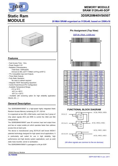
<strong>3D</strong><strong>SR20M40VS6507</strong><br />
20 Mbit SRAM organized as 512Kx40, based on 256Kx16<br />
Pin Assignment (Top View)<br />
SOP 84 (Pitch : 0.508 mm)<br />
Features<br />
- Fast Access Time : 12ns.<br />
- Power Supply 3.3V<br />
- Radiation Characteristics:<br />
Total Dose: 100Krad(Si)<br />
Immune to SEL (LET=110MeV.cm²/mg at 85°C)<br />
- TTL Compatible Input and Outputs.<br />
- Three State Outputs<br />
- Fully Static Operation<br />
No clock or refresh required<br />
- Integrate 100nF Decoupling capacitors<br />
- Centre Power/Ground Pin Configuration<br />
- Available Temperature Range:<br />
0°C to 70°C<br />
-40°C to +85°C<br />
-55°C to +125°C<br />
- Available with screening option for high reliability application<br />
(Space, etc…)<br />
General Description<br />
1 A9 22 Vss 43 A17 64<br />
2 A8 23 NC 44 A16 65<br />
#CS2<br />
#CS1<br />
3 A7 24 NC 45 A15 66 #CS0<br />
4 A6 25 Vcc 46 I/O15 67 NC<br />
5 A5 26 Vcc 47 I/O31 68 I/O35<br />
6 I/O7 27 Vcc 48 I/O14 69 I/O19<br />
7 I/O23 28 Vcc 49 I/O30 70 I/O3<br />
8 I/O39 29 Vcc 50 I/O13 71 I/O34<br />
9 I/O6 30 I/O27 51 I/O29 72 I/O18<br />
10 I/O22 31 I/O11 52 I/O12 73 I/O2<br />
11 I/O38 32 I/O26 53 I/O28 74 I/O33<br />
12 I/O5 33 I/O10 54 #OE3 75 I/O17<br />
13 I/O21 34 I/O25 55 #OE2 76 I/O1<br />
14 I/O37 35 I/O9 56 #OE1 77 I/O32<br />
15 I/O4 36 I/O24 57 #OE0 78 I/O16<br />
16 I/O20 37 I/O8 58 #WE0 79 I/O0<br />
17 I/O36 38 A14 59 #WE1 80 A4<br />
18 Vss 39 A13 60 #WE2 81 A3<br />
19 Vss 40 A12 61 #WE3 82 A2<br />
20 Vss 41 A11 62 NC 83 A1<br />
21 Vss 42 A10 63 #CS3 84 A0<br />
The <strong>3D</strong><strong>SR20M40VS6507</strong> is a high-speed highly integrated Static<br />
Random Access Memory containing 20, 971, 520 bit.<br />
It is organized as two 256 x 40bit banks, each bank has 2 group of<br />
chip select signals #CS and #WE to control the 32bit and 8bit<br />
independently .<br />
The <strong>3D</strong><strong>SR20M40VS6507</strong> uses 40 common input and output lines<br />
and has an output enable pin which operates faster than address<br />
access time at read cycle.<br />
The device is manufactured using <strong>3D</strong>-PLUS well known MCM-V<br />
patented technology designed for high speed circuit applications. It<br />
is particularity well suited for use in high reliability, high<br />
performance and high density system applications, such as solid<br />
state mass recorder, server or workstation.<br />
The <strong>3D</strong><strong>SR20M40VS6507</strong> is packaged in a 84 pin SOP.<br />
I/O 0-15<br />
I/O 16-31<br />
I/O 32-39<br />
FUNCTIONAL BLOCK DIAGRAM<br />
256<br />
x16<br />
256<br />
x16<br />
256<br />
x8<br />
#CS0, #WE0, #OE0<br />
#CS2, #CS2, #WE2, #WE2, #OE2 #OE3<br />
#CS1, #WE1, #OE1<br />
#CS3, #WE3, #OE3<br />
(All other signals are common to the six devices)<br />
SRAM Memory Module<br />
ALYSSON<br />
<strong>3D</strong>FP-0507-REV 4-Jun. 2011
Static Ram<br />
MODULE<br />
MEMORY MODULE<br />
SRAM 512Kx40-SOP<br />
<strong>3D</strong><strong>SR20M40VS6507</strong><br />
20 Mbit SRAM organized as 512Kx40, based on 256Kx16<br />
Mechanical Drawing<br />
Min<br />
Max<br />
A<br />
8.85 Max.<br />
A2<br />
7.3 Max.<br />
D 26.90 27.10<br />
E 28.55 28.95<br />
E1 26.05 26.25<br />
b 0.20<br />
e 0.508<br />
r 0.40<br />
Dimension (mm)<br />
Max. weight : 10.5gr.<br />
DC OPERATING CONDITIONS<br />
Parameter Symbol Min Typ Max Unit<br />
Supply Voltage V DD 3.0 3.3 3.6 V<br />
Input High Voltage V IH 2.0 V CC+0.3 V<br />
Input Low Voltage V IL -0.3 0.8<br />
Output High<br />
V OH 2.4 - V<br />
Voltage<br />
Output Low Voltage V OL - 0.4 V<br />
Note :<br />
Permanent device damage may occur if "ABSOLUTE MAXIMUM RATINGS"<br />
are exceeded.<br />
Functional operation should be restricted to recommended operating condition.<br />
Exposure to higher than recommended voltage for extended periods of time<br />
could affect device reliability<br />
ABSOLUTE MAXIMUM RATINGS<br />
Parameter Symbol Value Unit<br />
Voltage on any pin relative to V SS V T -0.5 to 4.6 V<br />
Storage temperature T STG -65 to +150 °C<br />
Power dissipation P D 3 W<br />
DC Characteristics<br />
Parameter Symbol Max Unit<br />
Operating Current (One bank active) I CC 450 mA<br />
TTL Standby Current I SB 240 mA<br />
CMOS Standby Current I SB1 30 mA<br />
<strong>3D</strong><strong>SR20M40VS6507</strong> - X X<br />
Temperature Range<br />
C = 0°C ~ +70°C<br />
I = -40°C ~ +85°C<br />
M = -55°C ~ +125°C<br />
Quality Level<br />
N = Commercial Grade<br />
B = Industrial Grade<br />
S = Space Grade<br />
Part Number Marking<br />
Part Option Marking<br />
Pin 1 Indicator<br />
Module Marking<br />
MMXX00000000XXX<br />
-XX 0000<br />
0000<br />
<strong>3D</strong> <strong>Plus</strong> Logo<br />
Date Code<br />
(WWYY) (YYWW )<br />
Serial Number<br />
(Optional)<br />
Main Sales Office<br />
FRANCE<br />
USA<br />
<strong>3D</strong> PLUS<br />
408, rue Hélène Boucher<br />
ZI.<br />
78532 BUC Cedex<br />
<strong>3D</strong> PLUS USA, Inc<br />
6633 Eldorado Parkway<br />
Suite 420<br />
Mckinney, TX 75070<br />
Tel : 33 (0)1 30 83 26 50 Fax : 33 (0)1 39 56 25 89<br />
Web : www.3d-plus.com<br />
e-mail : sales@3d-plus.com<br />
Tel : (241) 733-8505 Tel : (241) 733-8506 e-mail : sales@3d-plus.com<br />
DISTRIBUTOR<br />
SRAM Memory Module<br />
ALYSSON<br />
<strong>3D</strong>FP-0507-REV 4-Jun. 2011