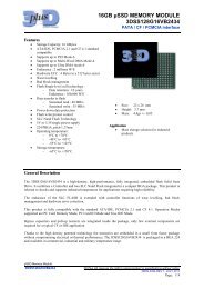
Double Data Rate SDRam MODULE - 3D Plus
Double Data Rate SDRam MODULE - 3D Plus
Double Data Rate SDRam MODULE - 3D Plus

Create successful ePaper yourself
Turn your PDF publications into a flip-book with our unique Google optimized e-Paper software.
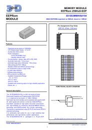
MEMORY <strong>MODULE</strong><br />
DDR <strong>SDRam</strong> 64Mx16-SOP<br />
<strong>Double</strong> <strong>Data</strong> <strong>Rate</strong> <strong>SDRam</strong><br />
<strong>MODULE</strong><br />
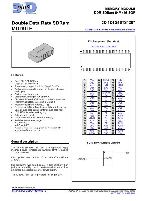
<strong>3D</strong> 1D1G16TS1267<br />
1Gbit DDR <strong>SDRam</strong> organized as 64Mx16<br />
Pin Assignment (Top View)<br />
SOP 66 (Pitch : 0.65 mm)<br />
Features<br />
One 1Gbit DDR <strong>SDRam</strong><br />
Organized as 64Mx16bit<br />
Power supply: V DD=2.5 ± 0.2V, V DDQ=2.5±0.2V<br />
<strong>Double</strong>-data-rate architecture; two data transfers per<br />
clock cycle<br />
Bi-directional data strobe<br />
Differential Clock input (CK and #CK)<br />
DLL aligns DQ and DQS transition with CK transition<br />
Programmable Read latency 2, 2.5 (clock)<br />
Programmable Burst length (2, 4, 8)<br />
Programmable Burst Type (sequential and interleave)<br />
Edge aligned data output, center aligned data input<br />
LDM, UDM for write masking only<br />
Auto and self refresh<br />
7.8 us refresh interval (8K/64ms refresh)<br />
Available temperature range :<br />
0°C to +70°C<br />
-40°C to +85°C<br />
Available with screening option for high reliability<br />
application (Space, etc …)<br />
1 V DD 23 #RAS 45 CK<br />
2 DQ0 24 #CS 46 #CK<br />
3 V DDQ 25 NC 47 UDM<br />
4 DQ1 26 BA0 48 V SS<br />
5 DQ2 27 BA1 49 V REF<br />
6 V SSQ 28 AP/A10 50 DNU<br />
7 DQ3 29 A0 51 UDQS<br />
8 DQ4 30 A1 52 V SSQ<br />
9 V DDQ 31 A2 53 NC<br />
10 DQ5 32 A3 54 DQ8<br />
11 DQ6 33 V DD 55 V DDQ<br />
12 V SSQ 34 V SS 56 DQ9<br />
13 DQ7 35 A4 57 DQ10<br />
14 NC 36 A5 58 V SSQ<br />
15 V DDQ 37 A6 59 DQ11<br />
16 LDQS 38 A7 60 DQ12<br />
17 A13 39 A8 61 V DDQ<br />
18 V DD 40 A9 62 DQ13<br />
19 DNU 41 A11 63 DQ14<br />
20 LDM 42 A12 64 V SSQ<br />
21 #WE 43 NC 65 DQ15<br />
22 #CAS 44 CKE 66 V SS<br />
General description<br />
FUNCTIONAL Block Diagram<br />
The <strong>3D</strong>-<strong>Plus</strong> <strong>3D</strong> 1D1G16TS1267 is a high-speed highly<br />
integrated DDR Synchronous Dynamic RAM containing<br />
1,073,741,824 bits.<br />
It is organized with one bank of 16bit with #CS, CKE, CK<br />
and #CK.<br />
64Mx16<br />
It is particularly well suited for use in high reliability, high<br />
performance and high density system applications, such as<br />
solid state mass recorder, server or workstation.<br />
The <strong>3D</strong> 1D1G16TS1267 is packaged in a 66 pin SOP.<br />
DDR Memory Module<br />
Preliminary / MMDD16064601STC<br />
<strong>3D</strong> <strong>Plus</strong> SA reserves the right to cancel product or specifications without notice<br />
<strong>3D</strong>FP-0267-RV 2-DEC 2008
MEMORY <strong>MODULE</strong><br />
DDR <strong>SDRam</strong> 64Mx16-SOP<br />
<strong>Double</strong> <strong>Data</strong> <strong>Rate</strong> <strong>SDRam</strong><br />
<strong>MODULE</strong><br />
<strong>3D</strong> 1D1G16TS1267<br />
1Gbit DDR <strong>SDRam</strong> organized as 64Mx16<br />
Min<br />
Max<br />
A - 4.05<br />
A2 - 2.80<br />
D 23.80 24.20<br />
E 13.40 13.80<br />
E1 10.85 11.05<br />
b 0.30<br />
e 0.65<br />
Dimension (mm)<br />
Max. weight : 2.4 gr.<br />
Test Tools<br />
<strong>3D</strong> 1D1G16TS1267 ENPLASOTS-_________ Modified by <strong>3D</strong> PLUS<br />
DC OPERATING CONDITIONS<br />
Parameter Symbol Min Max Unit<br />
Supply Voltage V DD<br />
2.5 2.7 V<br />
I/O Supply Voltage V DDQ<br />
2.5 2.7 V<br />
I/O Reference Voltage V REF<br />
0.49xV DDQ 0.51x V DDQ V<br />
I/O Termination<br />
V TT<br />
V REF –0.04 V REF +0.04 V<br />
Voltage (syst.)<br />
Input High Voltage V IH (DC) V REF +0.15 V REF +0.3 V<br />
Input . Low Voltage V IL (DC) -0.3 V REF -0.15 V<br />
Note :<br />
Permanent device damage may occur if "ABSOLUTE MAXIMUM RATINGS"<br />
are exceeded.<br />
Functional operation should be restricted to recommended operating condition.<br />
Exposure to higher than recommended voltage for extended periods of time<br />
could affect device reliability<br />
ABSOLUTE MAXIMUM RATINGS<br />
Parameter Symbol Value Unit<br />
Voltage on any pin relative to V SS V IN , V OUT<br />
-0.5 ~ +3.6 V<br />
Storage temperature T STG<br />
-55 ~ +150 °C<br />
Power dissipation P D<br />
1 W<br />
Short circuit current I OS<br />
50 mA<br />
DC Characteristics @ 133MHz<br />
Parameter Symbol Value Unit<br />
Operating Current (one bank active) I DD1<br />
195 mA<br />
Precharge Power Down Standby Current I DD2P<br />
10 mA<br />
Precharge Floating Standby Current I DD2F<br />
60 mA<br />
<strong>3D</strong> 1D1G16TS1267 X X<br />
Temperature Range<br />
C = 0°C ~ +70°C<br />
I = -40°C ~ +85°C<br />
M = -55°C ~ +125°C<br />
S = Specific<br />
Quality Level<br />
N = Commercial Grade<br />
B = Industrial Grade<br />
S = Space Grade<br />
C = Custom<br />
Main Sales Office<br />
FRANCE<br />
<strong>3D</strong> PLUS<br />
408, rue Hélène Boucher ZI.<br />
78532 BUC Cedex<br />
Tel : 33 (0)1 30 83 26 50 Fax : 33 (0)1 39 56 25 89<br />
Web : www.3d-plus.com<br />
e-mail : sales@3d-plus.com<br />
DISTRIBUTOR<br />
USA<br />
<strong>3D</strong> PLUS USA, Inc<br />
6633 Eldorado Parkway<br />
Suite 420<br />
Mckinney, TX 75070<br />
DDR Memory Module<br />
Preliminary / MMDD16064601STC<br />
Tel : (241) 733-8505 Tel : (241) 733-8506 e-mail : sales@3d-plus.com<br />
<strong>3D</strong> <strong>Plus</strong> SA reserves the right to cancel product or specifications without notice<br />
<strong>3D</strong>FP-0267-RV 2-DEC 2008