IBM 5150 PC Technical Reference (6025005, August, 1981) (PDF)
IBM 5150 PC Technical Reference (6025005, August, 1981) (PDF) IBM 5150 PC Technical Reference (6025005, August, 1981) (PDF)
N I ~ VI ) § I • \. ~ o el so. 0.. '"I -. 00 00 ~ . .... ~ ..., ::s ::T'N CD "0 :> "0 -. r.n -.::s r.n .... ~ 8 OQ o ~ ::scr ::s l:li o 9 ~§ ~ ~ ::s ::s g.~ ::s S 00 '"I ~
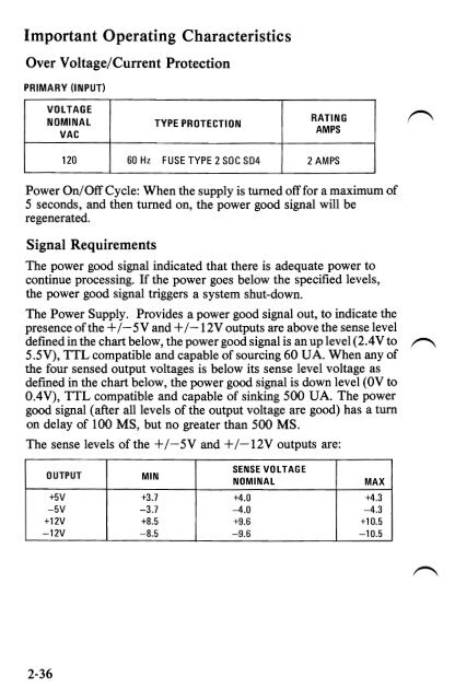
Important Operating Characteristics Over Voltage/Current Protection PRIMARY (INPUT) VOLTAGE NOMINAL VAC TYPE PROTECTION RATING AMPS 120 60 Hz FUSE TYPE 2 SOC SD4 2AMPS Power On/Off Cycle: When the supply is turned off for a maximum of 5 seconds, and then turned on, the power good signal will be regenerated. Signal Requirements The power good signal indicated that there is adequate power to continue processing. If the power goes below the specified levels, the power good signal triggers a system shut-down. The Power Supply. Provides a power good signal out, to indicate the presence ofthe +/-5V and +/-12Voutputs are above the sense level defined in the chart below, the power good signal is an up level (2.4V to 5 .5V), TTL compatible and capable of sourcing 60 VA. When any of the four sensed output voltages is below its sense level voltage as defined in the chart below, the power good signal is down level (OV to O.4V), TTL compatible and capable of sinking 500 VA. The power good signal (after all levels of the output voltage are good) has a turn on delay of 100 MS, but no greater than 500 MS. The sense levels of the +/-5V and +/-12V outputs are: "'" OUTPUT MIN SENSE VOLTAGE NOMINAL MAX +5V +3.7 +4.0 +4.3 -5V -3.7 -4.0 -4.3 +12V +8.5 +9.6 +10.5 -12V -8.5 -9.6 -10.5 2-36
- Page 5 and 6: FEDERAL COMMUNICATIONS COMMISSION R
- Page 8 and 9: CONTENTS SECTION 1. HARDWARE OVERV
- Page 10 and 11: Programming Considerations ........
- Page 12 and 13: INS 8250 Functional Pin Description
- Page 14 and 15: FIGURE LISTING 1. System Block Dia
- Page 16 and 17: SECTION I. HARDWARE OVERVIEW The
- Page 18 and 19: The 16KB Memory Expansion Kits allo
- Page 20 and 21: SECTION 2. HARDWARE ~ Contents: Sys
- Page 22 and 23: SYSTEM BOARD The System Board fits
- Page 24 and 25: The memory is dynamic 16K x 1 chips
- Page 26 and 27: System Board Data Flow Figure 2. S
- Page 28 and 29: 1/0 Channel Diagram REAR PANEl SI
- Page 30 and 31: I/O CHRDY I I/O Channel Ready: This
- Page 32 and 33: System Board Component Diagram REA
- Page 34 and 35: Keyboard Interface B lock Diagram
- Page 36 and 37: 1 2 3 4 5 6 7 8 9 10 11 12 13 14 15
- Page 38 and 39: Cassette User Interface The cassett
- Page 40 and 41: Cassette Interface Connector Specif
- Page 42 and 43: I/O Address Map HEX RANGE 9 8 7 6
- Page 44 and 45: System Memory Map X'OOOOO' 16 TO 6
- Page 46 and 47: System Memory Map Cont. START ADDR
- Page 48 and 49: 5-1/4" Diskette Drives Switch Setti
- Page 50 and 51: 32/64KB Memory Expansion Option Sw
- Page 52 and 53: Power Supply The system DC power su
- Page 56 and 57: IBM Monochrome Display and Parallel
- Page 58 and 59: System Channel Interface Lines Used
- Page 60 and 61: Programming Considerations Programm
- Page 62 and 63: • CRT Status Port (I/O Address '3
- Page 64 and 65: Color/Graphics Monitor Adapter The
- Page 66 and 67: CPU .. r-- ) ) ) DISPLAY ADDRESS BU
- Page 68 and 69: Modes of Operation There are two ba
- Page 70 and 71: IBM Monochrome Display Adapter V s.
- Page 72 and 73: Color selection is determined by th
- Page 74 and 75: 1"'"""""\ Table 5. I R G B Summary
- Page 76 and 77: Programming the Mode Control and St
- Page 78 and 79: Bit 5 When on, this bit will change
- Page 80 and 81: I/O Address and Bit Map Read/Write
- Page 82 and 83: Color/Graphics Monitor Adapter Auxi
- Page 84 and 85: Parallel Printer Adapter The Printe
- Page 86 and 87: Programming Considerations The Prin
- Page 88 and 89: Parallel Printer Adapter Interface
- Page 90 and 91: Table 7. Printer Specifications (1
- Page 92 and 93: Table 9. Functions and Conditions o
- Page 94 and 95: Table 10. Connector Pin Assignment
- Page 96 and 97: (4) Data transfer sequence Fig. 17
- Page 98 and 99: ASCII Control Codes Control Codes V
- Page 100 and 101: (8) DC 2 (Device Control 2) The DC
- Page 102 and 103: (b) 3) ESC 2 (Escape 2) Receipt of
Important Operating Characteristics<br />
Over Voltage/Current Protection<br />
PRIMARY (INPUT)<br />
VOLTAGE<br />
NOMINAL<br />
VAC<br />
TYPE PROTECTION<br />
RATING<br />
AMPS<br />
120 60 Hz FUSE TYPE 2 SOC SD4 2AMPS<br />
Power On/Off Cycle: When the supply is turned off for a maximum of<br />
5 seconds, and then turned on, the power good signal will be<br />
regenerated.<br />
Signal Requirements<br />
The power good signal indicated that there is adequate power to<br />
continue processing. If the power goes below the specified levels,<br />
the power good signal triggers a system shut-down.<br />
The Power Supply. Provides a power good signal out, to indicate the<br />
presence ofthe +/-5V and +/-12Voutputs are above the sense level<br />
defined in the chart below, the power good signal is an up level (2.4V to<br />
5 .5V), TTL compatible and capable of sourcing 60 VA. When any of<br />
the four sensed output voltages is below its sense level voltage as<br />
defined in the chart below, the power good signal is down level (OV to<br />
O.4V), TTL compatible and capable of sinking 500 VA. The power<br />
good signal (after all levels of the output voltage are good) has a turn<br />
on delay of 100 MS, but no greater than 500 MS.<br />
The sense levels of the +/-5V and +/-12V outputs are:<br />
"'"<br />
OUTPUT<br />
MIN<br />
SENSE VOLTAGE<br />
NOMINAL<br />
MAX<br />
+5V +3.7 +4.0 +4.3<br />
-5V -3.7 -4.0 -4.3 <br />
+12V +8.5 +9.6 +10.5 <br />
-12V -8.5 -9.6 -10.5 <br />
2-36


