Microstructure Analysis on Nanocrystalline Materials COMMISSION ...
Microstructure Analysis on Nanocrystalline Materials COMMISSION ...
Microstructure Analysis on Nanocrystalline Materials COMMISSION ...

You also want an ePaper? Increase the reach of your titles
YUMPU automatically turns print PDFs into web optimized ePapers that Google loves.
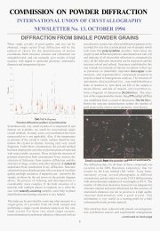
200 °C, not in the as-prepared state and <strong>on</strong>ly for copper<br />
samples.<br />
(a)<br />
(b)<br />
(c)<br />
(d)<br />
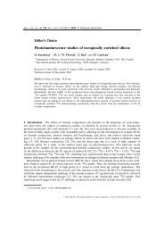
Fig. 8. Fragments of the Debye rings obtained by backreflecti<strong>on</strong><br />
for as-deformed sample Cu + 0.5 % Al2O3<br />
(a), the center of the same sample after annealing at<br />
550 °C (b), margin of the sample after annealing at<br />
550 °C (c), Fe sample after annealing at 550 °C.<br />
In Fig. 8, four cases are compared – rings for asdeformed<br />
state (a), for the central regi<strong>on</strong> of annealed<br />
sample (b), for outer regi<strong>on</strong> of the disc of the same<br />
sample (c) and for annealed ir<strong>on</strong> sample (d). Str<strong>on</strong>g inhomogeneity<br />
can be observed especially for copper<br />
while for ir<strong>on</strong> the distributi<strong>on</strong> of dots and c<strong>on</strong>sequently<br />
also grains is quite homogeneous. With increasing annealing<br />
temperature such effects can be seen <strong>on</strong> diffracti<strong>on</strong><br />
profiles as well. This also makes c<strong>on</strong>venti<strong>on</strong>al<br />
way of powder XRD line profile analysis impossible.<br />
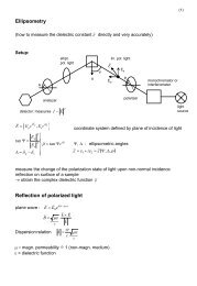
f(R)<br />
f(R)<br />
1000.0<br />
100.0<br />
10.0<br />
1.0<br />
0.1<br />
1.6e-4 1.0e1<br />
1.0e1<br />
8.0e0<br />
1.2e-4 8.0e0<br />
6.0e0<br />
6.0e0<br />
8.0e-5<br />
4.0e0<br />
4.0e0<br />
4.0e-5<br />
2.0e0<br />
2.0e0<br />
0.0e0<br />
Cu<br />
6 GPa, annealed at 250 °C for 4s<br />
-150 -100 -50 0 50 100 150 200<br />
Analyzer angle (arc sec<strong>on</strong>ds)<br />
Cu-250 4 4 ss<br />
Cu-250 4 s<br />
log-normal size size distributi<strong>on</strong><br />
log-normal size distributi<strong>on</strong><br />
0 2000 4000 6000 8000<br />
r(10 -10 0.0e0<br />
0 2000 4000 6000 8000<br />
r(10 m) -10 0.0e0<br />
0 2000 4000 6000 8000<br />
m)<br />
(b)<br />
Fig. 9. Experimental profile of the transmitted wave<br />
including diffuse scattering (thin line) and corresp<strong>on</strong>ding<br />
theoretical curve (fit, thick line) for the deformed<br />
copper annealed at 250 ºC (a), log-normal size distributi<strong>on</strong><br />
used for the calculati<strong>on</strong> of theoretical curve.<br />
A new method of measurements of the diffuse scattering<br />
by small crystallite size in the transmitted wave has<br />
been applied [31]. It c<strong>on</strong>sists in the comparis<strong>on</strong> of intensity<br />
profiles with and without diffuse scattering. It<br />
requires compact specimen with an appropriate thickness.<br />
It should be thick enough in order to measure the<br />
diffuse scattering but sufficiently thin in order to measure<br />
the transmitted intensity. For copper this means the<br />
sample thickness of about 0.1 mm. After careful<br />
alignment of the equipment with several crystal m<strong>on</strong>ochromators<br />
(to cut the tails of instrumental profile),<br />
23<br />
(a)