Microstructure Analysis on Nanocrystalline Materials COMMISSION ...
Microstructure Analysis on Nanocrystalline Materials COMMISSION ...
Microstructure Analysis on Nanocrystalline Materials COMMISSION ...

Create successful ePaper yourself
Turn your PDF publications into a flip-book with our unique Google optimized e-Paper software.
IN THIS ISSUE<br />
<str<strong>on</strong>g>Microstructure</str<strong>on</strong>g> <str<strong>on</strong>g>Analysis</str<strong>on</strong>g> <strong>on</strong> <strong>Nanocrystalline</strong> <strong>Materials</strong><br />
(David Rafaja, Editor)<br />
CPD Chairman’s message<br />
Bill David 2<br />
Editor’s message<br />
David Rafaja 2<br />
WWW sites related to Powder Diffracti<strong>on</strong> 2<br />
CPD Project 2<br />
IUCr Commissi<strong>on</strong> <strong>on</strong> Powder Diffracti<strong>on</strong> 3<br />
<str<strong>on</strong>g>Microstructure</str<strong>on</strong>g> <str<strong>on</strong>g>Analysis</str<strong>on</strong>g> <strong>on</strong> <strong>Nanocrystalline</strong> <strong>Materials</strong>:<br />
A Whole Powder Pattern Method for Nanoparticle Characterizati<strong>on</strong><br />
Ant<strong>on</strong>io Cervellino, Cinzia Giannini and<br />
Ant<strong>on</strong>ietta Guagliardi 4<br />
Practical Aspects of Partial Coherence of <strong>Nanocrystalline</strong><br />
Domains<br />
David Rafaja, Volker Klemm and Milan Dopita 7<br />
ISSN 1591-9552<br />
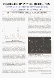
<strong>COMMISSION</strong> ON POWDER DIFFRACTION<br />
INTERNATIONAL UNION OF CRYSTALLOGRAPHY<br />
http://www.iucr-cpd.org/<br />
NEWSLETTER No. 34, December 2007<br />
http://www.iucr-cpd.org/Newsletters.htm<br />
The <str<strong>on</strong>g>Microstructure</str<strong>on</strong>g> of <strong>Nanocrystalline</strong> <strong>Materials</strong><br />
Determined by X-ray Line Profile <str<strong>on</strong>g>Analysis</str<strong>on</strong>g><br />
Tamás Ungár 13<br />
On Structural Studies of Sub-Microcrystalline<br />
<strong>Materials</strong> Obtained by Severe Plastic Deformati<strong>on</strong> –<br />
Thermal Stability and Inhomogeneity<br />
Radomír Kužel, Viktoria Cherkaska,<br />
Zdeněk Matěj, Jakub Čížek, Josef Pešička,<br />
Magsud Masimov and R.K. Islamgaliev 18<br />
New High-Temperature Furnace for SANS<br />
Measurements at DN-2 Double-Bent-Crystal<br />
Diffractometer in NPI Řež Near Prague<br />
Pavel Strunz, Jan Šaroun, Petr Lukáš,<br />
Pavol Mikula and Jakub Zrník 25<br />
Computer Corner<br />
Lachlan Cranswick 27<br />
News from the ICDD<br />
Jim Kaduk 29<br />
1
CPD Chairman’s Message<br />
Powder diffracti<strong>on</strong> is traditi<strong>on</strong>ally seen as a technique for the determinati<strong>on</strong> and refinement of moderately complex crystal<br />
structures that are difficult to prepare as single crystals for X-ray diffracti<strong>on</strong> analysis. Many people see powder diffracti<strong>on</strong> and<br />
the Rietveld technique as syn<strong>on</strong>ymous with <strong>on</strong>e another. However, there is an important class of materials where micr<strong>on</strong>-sized<br />
single crystals are simply not available – nanomaterials and nanocomposites. This current newsletter focuses <strong>on</strong> the developments<br />
and successes in using X-ray powder diffracti<strong>on</strong> to analyse nanocrystalline systems. High resoluti<strong>on</strong> and high statistical<br />
accuracy mean that precise, detailed structural and microstructural studies of nanomaterials may be performed using powder<br />
diffracti<strong>on</strong>. These reciprocal space studies complement and augment transmissi<strong>on</strong> electr<strong>on</strong> microscopy measurements and<br />
show that powder diffracti<strong>on</strong> has a relevance to the real world that ranges from nanometre to millimetre lengthscales.<br />
From the Editor of Newsletter 34<br />
Bill David<br />
For microstructure analysis <strong>on</strong> nanocrystalline materials and nanocomposites, transmissi<strong>on</strong> electr<strong>on</strong> microscopy is the technique<br />
of choice. However, in this issue of the Commissi<strong>on</strong> <strong>on</strong> Powder Diffracti<strong>on</strong> Newsletter, we show that recent developments<br />
in instrumentati<strong>on</strong> and analysis mean that X-ray powder diffracti<strong>on</strong> still has a huge potential. Indeed, it is <strong>on</strong>ly the combinati<strong>on</strong><br />
of these experimental methods, supplemented by other techniques such as spectroscopy that yields a complete understanding<br />
of the microstructure of nanomaterials.<br />
Traditi<strong>on</strong>al advantages of the powder X-ray diffracti<strong>on</strong> are its high statistical relevance and the n<strong>on</strong>-destructive nature of the<br />
sample preparati<strong>on</strong>, which still favour the powder X-ray diffracti<strong>on</strong> in comparis<strong>on</strong> with the transmissi<strong>on</strong> electr<strong>on</strong> microscopy.<br />
Other advantages of the powder X-ray diffracti<strong>on</strong> are the excellent resoluti<strong>on</strong> in reciprocal space and high sensitivity to the<br />
crystal anisotropy of the interplanar spacing and its changes that are much better than for TEM.<br />
The papers in this issue present diffracti<strong>on</strong> phenomena and experimental results obtained over several orders of magnitude:<br />
from clusters of atoms (individual nanocrystallites) and of partially coherent nanocrystallites, through nanocrystallites c<strong>on</strong>taining<br />
structure defects to sub-microcrystalline materials obtained by severe plastic deformati<strong>on</strong> and precipitates with mutual distances<br />
in sub-micrometer range.<br />
David Rafaja<br />
WWW sites related to powder diffracti<strong>on</strong><br />
The Commissi<strong>on</strong> <strong>on</strong> Powder Diffracti<strong>on</strong> (CPD): http://www.iucr-cpd.org/<br />
The Internati<strong>on</strong>al Uni<strong>on</strong> of Crystallography (IUCr): http://www.iucr.org/<br />
The Internati<strong>on</strong>al Centre for Diffracti<strong>on</strong> Data (ICDD): http://www.icdd.com/<br />
The Internati<strong>on</strong>al X-ray <str<strong>on</strong>g>Analysis</str<strong>on</strong>g> Society (IXAS): http://www.ixas.org/<br />
Collaborative Computati<strong>on</strong>al Project #14 (CCP 14): http://www.ccp14.ac.uk/<br />
Submitting a proposal for neutr<strong>on</strong> diffracti<strong>on</strong> or synchrotr<strong>on</strong> radiati<strong>on</strong> X-ray diffracti<strong>on</strong> is possible at many (publicly funded)<br />
large scale facilities in the world. It represents an important and frequently unique opportunity for powder diffracti<strong>on</strong> experiments.<br />
A useful guide and informati<strong>on</strong> can be accessed through the following web-site, maintained by R. Dinnebier at<br />
http://www.pulverdiffraktometrie.de/. This list is far from being complete and needs input from users and readers of the CPD<br />
Newsletter. Please send comments to R. Dinnebier (r.dinnebier@fkf.mpg.de)<br />
CPD project<br />
Rietveld refinement of organic structures<br />
Increasing numbers of organic crystal structures are being solved and refined from powder diffracti<strong>on</strong> data. The basic arrangement<br />
of the molecules in the structure can often be determined by direct methods, or by direct-space approaches. However,<br />
experience shows that problems can arise in the subsequent Rietveld refinement. For example, unless restrained by appropriate<br />
b<strong>on</strong>d distances and angles molecules can distort unrealistically from a reas<strong>on</strong>able molecular structure. So how good<br />
are these Rietveld refinements? Is the problem a fundamental <strong>on</strong>e of powder diffracti<strong>on</strong>? e.g. the ambiguities and correlati<strong>on</strong>s<br />
caused by peak overlap or defining the background etc. lead to inaccurate structures. Or can some of the blame be attributed to<br />
poor refinement practice? We plan to put <strong>on</strong>to the CPD web site a number of good quality powder diffracti<strong>on</strong> patterns from<br />
organic compounds of known crystal structure and of different complexity. These can be downloaded, and powder crystallographers<br />
can try out their own prowess at Rietveld refinement, by comparing their refined structures with the accepted singlecrystal<br />
structures. This should be a learning exercise for us all. Any suggesti<strong>on</strong>s as to compounds that would appear particularly<br />
appropriate for this project are very welcome. Please c<strong>on</strong>tact the CPD chairman, Bill David, at bill.david@rl.ac.uk.<br />
2
THE IUCR <strong>COMMISSION</strong> ON POWDER DIFFRACTION - TRIENNIUM 2005-2008<br />
Chairman: Prof. W. I. F. David (Bill)<br />
Rutherford Applet<strong>on</strong> Laboratory (CCLRC), Chilt<strong>on</strong>, Ox<strong>on</strong><br />
OX11 OQX, United Kingdom<br />
Teleph<strong>on</strong>e: +44 1235 445179 | Fax: +44 1235 445642<br />
e-mail: W.I.F.David@rl.ac.uk<br />
Secretary: Prof. A. N. Fitch (Andy)<br />
ESRF, BP220, F-38043 Grenoble Cedex 9, France<br />
Teleph<strong>on</strong>e : +33 476 88 25 32 | Fax: +33 476 88 25 42<br />
e-mail: fitch@esrf.fr<br />
Prof. S.J.L. Billinge (Sim<strong>on</strong>)<br />
Department of Physics and Astr<strong>on</strong>omy,<br />
Michigan State University, East Lansing, MI 48824,<br />
U.S.A.<br />
Teleph<strong>on</strong>e: +1 517 353 8697 | Fax: +1 517 353 4500<br />
e-mail: billinge@pa.msu.edu<br />
Prof. M. Delgado (Miguel)<br />
Laboratorio de Cristalografía, Departamento de Química,<br />
Facultad de Ciencias, Universidad de Los Andes, P.O. Box<br />
40, La Hechicera, Mérida 5251, Venezuela<br />
Teleph<strong>on</strong>e: +58 274 240 1372 | Fax: +58 274 240 1286<br />
e-mail: migueld@ula.ve<br />
Dr. I. Madsen (Ian)<br />
CSIRO Minerals<br />
Box 312, Clayt<strong>on</strong> South 3169, Victoria, Australia<br />
Teleph<strong>on</strong>e: +61 3 9545 8785 | Fax: +61 3 9562 8919<br />
e-mail: Ian.Madsen@csiro.au<br />
Prof. N. Masciocchi (Norberto)<br />
Dipartimento di Scienze Chimiche e Ambientali,<br />
Università dell' Insubria, via Valleggio 11, I-22100 Como,<br />
Italy<br />
Teleph<strong>on</strong>e: +39 031 326227 | Fax: +39-031-2386119<br />
e-mail: norberto.masciocchi@uninsubria.it<br />
Prof. D. Rafaja (David)<br />
Institut für Werkstoffwissenschaft, TU Bergakademie Freiberg,<br />
Gustav-Zeuner-Str. 5, D-09599 Freiberg,<br />
Germany<br />
Teleph<strong>on</strong>e: +49 3731 39 2299 | Fax: +49 3731 39 3657<br />
e-mail: Rafaja@ww.tu-freiberg.de<br />
Dr. R. Rizzi (Rosanna)<br />
CNR IC – c/o Dip. Geomineralogico, Via Orab<strong>on</strong>a 4,<br />
I-70125 Bari, Italy<br />
Teleph<strong>on</strong>e: + 39 80 544 2624 | Fax: + 39 80 544 2591<br />
e-mail: rosanna.rizzi@ic.cnr.it<br />
Prof. P. Stephens (Peter)<br />
Department of Physics and Astr<strong>on</strong>omy<br />
St<strong>on</strong>y Brook University, St<strong>on</strong>y Brook, NY 11794-3800,<br />
USA<br />
Teleph<strong>on</strong>e: +1 631 632 8156 | Fax: +1 631 632 4977<br />
e-mail: pstephens@notes.cc.sunysb.edu<br />
Dr. P. Whitfield (Pam)<br />
Institute for Chemical Process and Envir<strong>on</strong>mental Technology,<br />
Nati<strong>on</strong>al Research Council Canada, Building M12, 1200<br />
M<strong>on</strong>treal Road, Ottawa, Ontario, K1A 0R6, Canada<br />
Teleph<strong>on</strong>e: +1 613 998 8462 | Fax: +1 613 991 2384<br />
e-mail: Pamela.Whitfield@cnrc-nrc.gc.ca<br />
C<strong>on</strong>sultants<br />
Dr. J. Cline (Jim)<br />
Ceramics Divisi<strong>on</strong> (852), NIST, 100 Bureau Drive,<br />
Stop 8520, Gaithersburg, MD 20899, USA<br />
Teleph<strong>on</strong>e: +1 301 975 5793<br />
e-mail: james.cline@nist.gov<br />
Dr. R. E. Dinnebier (Robert)<br />
Max-Planck-Institut für Festkörperforschung,<br />
Heisenbergstrasse 1, D-70569 Stuttgart, Germany<br />
Teleph<strong>on</strong>e: +49 711 689 1503 | Fax: +49 711 689 1502<br />
e-mail: r.dinnebier@fkf.mpg.de<br />
Prof. P. Scardi (Paolo)<br />
Dipartimento di Ingegneria dei Materiali e Tecnologie<br />
Industriali, Università di Trento, I-38050 Mesiano (TN), Italy<br />
Teleph<strong>on</strong>e: +39 0461 882417/67 | Fax: +39 0461 881977<br />
e-mail: Paolo.Scardi@ing.unitn.it<br />
Prof. J. De Villiers (Johan)<br />
Mineral Divisi<strong>on</strong> MINTEK, Private Bag X3015, Randburg<br />
2125, South Africa<br />
Teleph<strong>on</strong>e: +27 11 709 4745 | Fax: +27 11 709 4564<br />
e-mail: jpdev@postino.up.ac.za<br />
Dr. I. Margiolaki (Irene)<br />
ESRF, BP 220, F-38043 Grenoble Cedex, France<br />
Teleph<strong>on</strong>e: +33 476 88 2148 | Fax: +33 476 88 2907<br />
e-mail: margiolaki@esrf.fr<br />
Prof. M. Yashima (Masatomo)<br />
Tokyo Institute of Technology, Grad. School of Science and<br />
Engineering, Department of <strong>Materials</strong> Science and Engineering,<br />
Nagatsuta-cho 4259-J1-4,<br />
Midori-ku Yokohama, 226-8502, Japan<br />
Teleph<strong>on</strong>e: +81-45-924-5630 | Fax: +81-45-924-5630<br />
e-mail: yashima@materia.titech.ac.jp<br />
ICDD Representative<br />
Dr. J. Kaduk (Jim)<br />
INEOS Technologies, Analytical Science Research Services,<br />
MC F-9, P.O. Box 3011, 150 W. Warrenville Road,<br />
Naperville IL 60566-7011<br />
Teleph<strong>on</strong>e: +1 630 420 4547 | Fax: +1 630 420 5252<br />
e-mail: james.kaduk@innovene.com<br />
3<br />
3
A WHOLE POWDER PATTERN METHOD FOR<br />
NANOPARTICLE CHARACTERIZATION<br />
Ant<strong>on</strong>io Cervellino 1,* , Cinzia Giannini 2 , Ant<strong>on</strong>ietta<br />
Guagliardi 2<br />
1. Laboratory for Neutr<strong>on</strong> Scattering, ETH Zurich and<br />
PSI Villigen, CH-5232 Villigen PSI, Switzerland<br />
2. Istituto di Cristallografia, CNR<br />
Via Amendola 122/O, 70126 Bari, ITALY<br />
e-mail: cinzia.giannini@ic.cnr.it<br />
INTRODUCTION<br />
The quantitative analysis of powder diffracti<strong>on</strong> patterns<br />
collected <strong>on</strong> nanocrystals c<strong>on</strong>stitutes a complex problem<br />
of data analysis. Significant differences distinguish<br />
a nanomaterial from a micrometric <strong>on</strong>e, as summarized<br />
in Fig. 1. A c<strong>on</strong>tributi<strong>on</strong> to the pattern of utmost importance<br />
comes from the size (and the size distributi<strong>on</strong>),<br />
especially for very small particles (1-2 nm), where the<br />
diffracti<strong>on</strong> peak width can reach several degrees. Another<br />
important c<strong>on</strong>tributi<strong>on</strong> derives from the surface.<br />
At extremely small sizes the ratio of surface to volume<br />
atoms may easily exceed 50% (see Fig. 1). Surface<br />
atom positi<strong>on</strong>s differ from the bulk because of rec<strong>on</strong>structi<strong>on</strong>,<br />
and, in additi<strong>on</strong>, due to the surface strain<br />
fields that normally occur due to surfactants. This surface<br />
effect is size dependent. Therefore, at least a size<br />
dependent unit cell should be modelled to account for<br />
the surface effect [1]. In some specific cases, such as<br />
for noble metals, a nanocrystalline sample is realistically<br />
composed by more structures; some of them even<br />
n<strong>on</strong> crystallographic (icosahedra, decahedra). The latter<br />
cannot be described as a porti<strong>on</strong> of a periodic lattice<br />
and have a five-fold symmetry axis. This further level<br />
of complexity rules out any traditi<strong>on</strong>al crystallographic<br />
method.<br />
Fig. 1. Schematic illustrati<strong>on</strong> of the most important<br />
features of nanocrystalline sample.<br />
Finally, a complete method should be able to treat<br />
nanoparticles of whatever shape (sphere, rod, tetrapod<br />
etc) as needed for many technological compounds recently<br />
synthesized. Especially for larger nanoparticles,<br />
defects (stacking faults, anti-phase domains etc) are<br />
also expected and should be added into the model.<br />
These are the most important aspects to c<strong>on</strong>sider for<br />
making a method of quantitative microstructural analysis<br />
successful for nanocrystals. Our choice has been to<br />
use the Debye functi<strong>on</strong> (DF) for the diffracted intensity<br />
calculati<strong>on</strong>. This choice was firstly motivated by the<br />
need to treat diffracti<strong>on</strong> data collected <strong>on</strong> noble metals,<br />
as the Debye functi<strong>on</strong> does not require lattice periodicity.<br />
Additi<strong>on</strong>al advantages of the DF pattern calculati<strong>on</strong><br />
with respect to the shape-based c<strong>on</strong>voluti<strong>on</strong> approach<br />
[7] c<strong>on</strong>vinced us to select this method as the most appropriate<br />
approach for structural analysis <strong>on</strong> nanocrystals.<br />
In the following, we will briefly describe the<br />
method and give some applicati<strong>on</strong>s.<br />
FROM THE CLUSTER TO THE PATTERN<br />
Few basic steps have to be fulfilled to calculate the diffracti<strong>on</strong><br />
pattern:<br />
1. C<strong>on</strong>structing the atomic models for clusters of increasing<br />
size up to a maximum diameter provided<br />
by the user. In the case of spherical shape, clusters<br />
are made of c<strong>on</strong>centric shells added in discrete<br />
numbers (<strong>on</strong>i<strong>on</strong>-like model). The size step corresp<strong>on</strong>ds<br />
to a spherical shell whose volume c<strong>on</strong>tains<br />
an entire number of formula units.<br />
2. Calculating the corresp<strong>on</strong>ding interatomic distances<br />
database. Our approach has been to generate few<br />
databases corresp<strong>on</strong>ding to some relevant crystallographic<br />
prototypes (diam<strong>on</strong>d, rocksalt, fcc, rutile,<br />
zincblende and wurtzite [2]) as well as to generate<br />
the databases for some n<strong>on</strong> crystallographic structures<br />
(icosahedra, decahedra and truncated decahedra).<br />
Any nanocrystal having <strong>on</strong>e of the listed<br />
prototypes, or alternatively, any m<strong>on</strong>o-atomic noble<br />
metal (Au, Ag) which is known to crystallize in fcc<br />
but also according to other n<strong>on</strong> crystallographic<br />
structures, can be treated within this approach. It is<br />
necessary to select the correct database, re-scale the<br />
interatomic distances using the proper unit cell and<br />
substitute the proper atomic species.<br />
3. For each structure in the sample a log-normal size<br />
distributi<strong>on</strong> and size dependent strain distributi<strong>on</strong><br />
have to be provided. In the case of nanocrystals of<br />
spherical shape, a uniform and isotropic surface-led<br />
radial deformati<strong>on</strong> inside each single nanoparticle<br />
was chosen as strain functi<strong>on</strong>.<br />
The shortcoming of this approach is the huge number<br />
of distances to be c<strong>on</strong>sidered, even grouping the equal<br />
<strong>on</strong>es, with grim perspective with respect to the calculati<strong>on</strong><br />
times and the possibility of applying iterative optimisati<strong>on</strong><br />
algorithms like n<strong>on</strong> linear least-squares.<br />
Therefore, a distances sampling algorithm, inspired to<br />
Ten Eyck's idea [3], is applied to each database: each<br />
distance is c<strong>on</strong>voluted in direct space with a Gaussian<br />
functi<strong>on</strong>, summing up all these Gaussian functi<strong>on</strong>s to<br />
obtain a c<strong>on</strong>tinuous atomic pair distance distributi<strong>on</strong><br />
(PDF), which is then sampled <strong>on</strong> a fixed grid with a<br />
suitable step δ (δ < Δ, the width of Gaussians). The<br />
number of interatomic distances is drastically reduced<br />
by sampling, as shown in Table I, choosing Au<br />
nanocrystals in the icosahedral structure.<br />
4
Once the sampled interatomic distance database is<br />
available and the size and strain distributi<strong>on</strong> functi<strong>on</strong>s<br />
are chosen, the pattern intensity can be easily computed<br />
using a fast algorithm performing the Debye Functi<strong>on</strong>,<br />
thanks to the c<strong>on</strong>stant step of the sampled distances [4].<br />
The details of the pattern intensity calculati<strong>on</strong> and interatomic<br />
distances sampling are given in [4, 5]. A<br />
brief descripti<strong>on</strong> of the software NANO which presently<br />
implements our method is described in [6]. With<br />
respect to the versi<strong>on</strong> described in [6] the refinement<br />
secti<strong>on</strong> has been modified alternating COMPLEX,<br />
Simulating Annealing and Full-Newt<strong>on</strong> Least Squares<br />
algorithms.<br />
n d(nm) Atoms Interatomic<br />
distances<br />
Gaussian<br />
sampled<br />
distances<br />
5 2.143 561 1.6 · 105 5 2.143 561 1.6 · 10 362<br />
5 5 2.143 561 1.6 · 10 362<br />
5 1.6 · 105 362<br />
10 4.524 3871 7.5 · 106 10 4.524 3871 7.5 · 10 705<br />
6 10 4.524 3871 7.5 · 10 705<br />
6 7.5 · 106 705<br />
20 9.286 28741 4.0 · 108 20 9.286 28741 4.0 · 10 1412<br />
8 20 9.286 28741 4.0 · 10 1412<br />
8 4.0 · 108 1412<br />
50 23.573 429351 9.0 · 10 10 50 23.573 429351 9.0 · 10 3534<br />
10 50 23.573 429351 9.0 · 10 3534<br />
10 9.0 · 10 10 3534<br />
Table I. n = cluster shell number, d = cluster diameter,<br />
interatomic distances and Gaussian sampled distances<br />
valid up to 2 sinθ<br />
max<br />
−1<br />
q max = = 125 . Å .<br />
λ<br />
APPLICATIONS<br />
PbS nanoparticles<br />
Colloidals PbS nanoparticles in the size range 4-7 nm<br />
have been studied by HRTEM and XRPD to determine<br />
the particle size in order to calculate the extincti<strong>on</strong> coefficients<br />
[7]. One of the samples involved in this work<br />
was analyzed with this approach (an extensive applicati<strong>on</strong><br />
was not possible because the samples are all affected<br />
by texture effects, not yet available in the<br />
model). We generated spherical PbS clusters up to<br />
about 20 nm in diameter (prototype rocksalt, Pears<strong>on</strong><br />
symbol cF8). The structural informati<strong>on</strong> was taken by<br />
ICSD #38293, with a cell parameter a=5.934 Å.<br />
Intensity<br />
8000<br />
7000<br />
6000<br />
5000<br />
4000<br />
3000<br />
2000<br />
1000<br />
0<br />
-1000<br />
Fracti<strong>on</strong> (%)<br />
Fig. 2. PbS XRPD experimental dataset and relevant<br />
calculated pattern. Background and difference profiles<br />
are included. Size & Strain distributi<strong>on</strong> are shown in<br />
the inset. GoF=2.54, Rwp=10.32.<br />
60<br />
50<br />
40<br />
30<br />
20<br />
10<br />
30 40 50 60 70 80 90<br />
2θ (deg)<br />
0<br />
0.990<br />
5 6 7 8 9 10<br />
diameters (nm)<br />
1.010<br />
1.008<br />
1.006<br />
1.004<br />
1.002<br />
1.000<br />
0.998<br />
0.996<br />
0.994<br />
0.992<br />
Strain<br />
Refined parameters were: the centre and width of the<br />
lognormal size distributi<strong>on</strong>, strain parameters and the<br />
background coefficients. The final best fit is shown in<br />
Fig. 2 together with the size and strain distributi<strong>on</strong>s (in<br />
the inset).<br />
The tensile strain of about 0.001, independent<br />
of the size, can be also interpreted as a larger unit cell<br />
(a = 5.942 Å) in agreement with the refined value that<br />
was found when the data were modelled using a shapebased<br />
c<strong>on</strong>voluti<strong>on</strong> approach described in [8].<br />
Ir<strong>on</strong> oxide nanoparticles<br />
Maghemite nanoparticles have been synthesized with<br />
an original chemical route obtaining nanocrystals of<br />
different shapes according to the reacti<strong>on</strong> parameters<br />
[9]. In Fig. 3 the diffracti<strong>on</strong> patterns collected <strong>on</strong><br />
spherical shape nanocrystals (solid line) and <strong>on</strong><br />
tetrapods (dotted curve) are shown. The shape clearly<br />
affects the width and intensity ratio. A gradual increase<br />
in the I220/I511 and especially in the I440/I311 ratio accompanies<br />
the transiti<strong>on</strong> from the spherical to the<br />
tetrapod shape with progressively l<strong>on</strong>ger branches. It is<br />
also noted that the (111) and (220) peak maxima<br />
slightly shift to higher angles. We first started data analy-<br />
sis with the sample having a spherical shape.<br />
Within our approach we generated spherical<br />
maghemite clusters up to about 10 nm in diameter. The<br />
structural informati<strong>on</strong> 1 was taken by ICSD #87119<br />
(Pears<strong>on</strong> symbol cP53), with a cell parameter a =<br />
8.3457 Å. Refined parameters were: centre and width<br />
of the lognormal size distributi<strong>on</strong>, the isotropic thermal<br />
parameters and the background coefficients. The final<br />
best fit is shown in Fig. 4 together with the size and<br />
strain distributi<strong>on</strong>s (in the inset).<br />
Intensity<br />
18000<br />
16000<br />
14000<br />
12000<br />
10000<br />
8000<br />
6000<br />
4000<br />
2000<br />
0<br />
111<br />
220<br />
311<br />
222<br />
400<br />
422<br />
511<br />
440<br />
620<br />
533<br />
444<br />
642<br />
731<br />
800<br />
751<br />
840<br />
10 20 30 40 50<br />
2θ (deg)<br />
Fig. 3. Ir<strong>on</strong> Oxide XRPD experimental datasets: the<br />
solid and dotted lines corresp<strong>on</strong>d to spherical and<br />
tetrapod shape nanocrystals, respectively.<br />
The atomic models for tetrapods (TPs) with arms oriented<br />
al<strong>on</strong>g the [110], [111] and [100] orientati<strong>on</strong>s<br />
were generated and the corresp<strong>on</strong>ding diffracti<strong>on</strong> patterns<br />
were calculated. Dotted and solid curves are<br />
computed for TPs with different arm length (l) and di-<br />
1 It is worth noting that for this structure, cluster's generati<strong>on</strong><br />
takes into account the partial occupancy of<br />
some atoms.<br />
931<br />
844<br />
5
ameter (d): l = 20Å, d = 150Å (dotted) and l = 40Å, d =<br />
180Å (solid). The comparis<strong>on</strong> shows the different effect<br />
<strong>on</strong> the reflecti<strong>on</strong>s width according to the arm orientati<strong>on</strong>s<br />
and dimensi<strong>on</strong>s.<br />
Intensity<br />
7000<br />
6000<br />
5000<br />
4000<br />
3000<br />
2000<br />
1000<br />
0<br />
Fracti<strong>on</strong> (%)<br />
0<br />
0.990<br />
4 5 6<br />
-1000<br />
10 20 30 40 50<br />
90<br />
60<br />
30<br />
2θ (deg)<br />
diameters (nm)<br />
Fig. 4. Ir<strong>on</strong> oxide XRPD experimental dataset and<br />
relative calculated pattern. Background and difference<br />
profiles are included. Size & Strain distributi<strong>on</strong> are<br />
shown in the inset. GoF = 2.43, Rwp = 6.79.<br />
20000<br />
15000<br />
10000<br />
5000<br />
0<br />
20000<br />
15000<br />
10000<br />
5000<br />
0<br />
20000<br />
15000<br />
10000<br />
5000<br />
0<br />
111<br />
111<br />
111<br />
220<br />
10 20<br />
2θ (deg)<br />
30<br />
220<br />
10 20<br />
2θ (deg)<br />
30<br />
220<br />
311<br />
222<br />
311<br />
222<br />
311<br />
222<br />
400<br />
400<br />
400<br />
422<br />
511<br />
422<br />
511<br />
422<br />
511<br />
440<br />
440<br />
440<br />
10 20<br />
2θ (deg)<br />
30<br />
1.010<br />
1.008<br />
1.006<br />
1.004<br />
1.002<br />
1.000<br />
0.998<br />
0.996<br />
0.994<br />
0.992<br />
Strain<br />
TETRA110<br />
620<br />
533<br />
444<br />
TETRA111<br />
620<br />
533<br />
444<br />
TETRA100<br />
620<br />
533<br />
444<br />
Fig. 5. Calculated patterns for TPs with arms oriented<br />
The increase of the I440/I311 ratio as well as the (111)<br />
and (220) peak shift to higher angles, experimentally<br />
found, can be explained by a coexistence of TPs oriented<br />
both al<strong>on</strong>g the [111] and the [110], ruling out the<br />
[100] <strong>on</strong>e. Tetrapods had been found with arms preferentially<br />
oriented al<strong>on</strong>g the [111] directi<strong>on</strong>s by transmissi<strong>on</strong><br />
electr<strong>on</strong> microscopy (TEM). Therefore, XRPD<br />
analysis c<strong>on</strong>firmed TEM findings but adding a precious<br />
informati<strong>on</strong>.<br />
PERSPECTIVES<br />
Nowadays, the size and shape evoluti<strong>on</strong> of colloidal<br />
nanocrystals, driven by both thermodynamic parameters<br />
and kinetically-limited growth processes, is attempting<br />
to assemble different materials together in<br />
heterostructures (hybrid materials) playing with crystal<br />
miscibility, interfacial strain, and face-selective reactivity.<br />
The structural and compositi<strong>on</strong>al c<strong>on</strong>trol of the resulting<br />
architecture is fundamental. Therefore powerful<br />
structural investigati<strong>on</strong> tools are highly required. It is<br />
worth noting that fairly large amounts of material are<br />
produced and have to be c<strong>on</strong>trolled. In this respect,<br />
powder diffracti<strong>on</strong> analysis has been showing to grant<br />
a rapid and cheap answer in terms of size, strain, shape<br />
and structure characterizati<strong>on</strong>. Relative data treatment<br />
methodologies are in c<strong>on</strong>tinuous development and improvement<br />
to guarantee the most complete and reliable<br />
informati<strong>on</strong>. Critical aspects are the treatment of exotic<br />
shapes as well as the occurrence of defects. Further<br />
work is in progress to extend and complete the present<br />
theoretical approach.<br />
The most important parts of software – as a<br />
program suite – are to be made available under GPL<br />
(Gnu Public License).<br />
REFERENCES<br />
* On leave from the Istituto di Cristallografia -CNR-<br />
Bari, Italy<br />
[1] R. Lamber, S. Wetjen, I. Jaeger, Phys. Rev. B 51<br />
(1995) 10968.<br />
[2] http://cst-www.nrl.navy.mil/lattice/prototype.html<br />
[3] F.L. Ten Eyck, Acta Cryst. A33 (1977) 486.<br />
[4] A. Cervellino, C. Giannini, A. Guagliardi, J. Appl.<br />
Cryst. 36 (2003) 1148.<br />
[5] A. Cervellino, C. Giannini, A. Guagliardi, J. Comp.<br />
Chem. 27 (2006) 998.<br />
[6] A. Cervellino, C. Giannini, A. Guagliardi, CPD<br />
Newsletter 30 (2005).<br />
[7] L. Cademartiri, E. M<strong>on</strong>tanari, G. Calestani, A. Migliori,<br />
A. Guagliardi, G.A. Ozin, J. Amer. Chem. Soc.<br />
(2006) in press.<br />
[8] A. Cervellino, C. Giannini, A. Guagliardi, M.<br />
Ladisa, Phys. Rev. B 72 (2005) 035412.<br />
al<strong>on</strong>g the [110], [111] and [100] orientati<strong>on</strong>s. [9] P.D. Cozzoli, E. Snoeck, M.A. Garcia, C. Giannini,<br />
A. Guagliardi, A. Cervellino, F. Gozzo, A. Hernando,<br />
K. Achterhold, F.G. Parak, R. Cingolani, L.<br />
Manna, Nanoletters 6 (2006) 1966.<br />
6
PRACTICAL ASPECTS OF PARTIAL COHER-<br />
ENCE OF NANOCRYSTALLINE DOMAINS<br />
David Rafaja, Volker Klemm and Milan Dopita *<br />
Institute of <strong>Materials</strong> Science, TU Bergakademie Freiberg,<br />
Gustav-Zeuner-Str. 5, D-09599 Freiberg, Germany,<br />
E-mail: rafaja@ww.tu-freiberg.de<br />
ABSTRACT<br />
Partial coherence of crystallites is often observed in<br />
supra-hard nanocomposites having a str<strong>on</strong>g texture as<br />
an effect causing the diffracti<strong>on</strong> line “narrowing”. The<br />
degree of the partial coherence depends <strong>on</strong> the crystallite<br />
size, <strong>on</strong> the local preferred orientati<strong>on</strong> of crystallites<br />
and <strong>on</strong> the size of the diffracti<strong>on</strong> vector. C<strong>on</strong>sequently,<br />
the microstructure parameters influencing the<br />
partial coherence of crystallites can be determined from<br />
the dependence of the diffracti<strong>on</strong> line broadening <strong>on</strong><br />
the size of the diffracti<strong>on</strong> vector. In some thermodynamically<br />
unstable systems, like in Ti-Al-Si-N and Cr-<br />
Al-Si-N thin films, the str<strong>on</strong>gly correlated orientati<strong>on</strong><br />
of adjacent crystallites that is a necessary c<strong>on</strong>diti<strong>on</strong> for<br />
their partial coherence can be understood as an indicator<br />
of the spinodal decompositi<strong>on</strong>.<br />
INTRODUCTION<br />
<strong>Nanocrystalline</strong> materials are employed in many industrial<br />
applicati<strong>on</strong>s, e.g. in materials for catalytic c<strong>on</strong>verters,<br />
in producti<strong>on</strong> of self cleaning surfaces, in magnetic<br />
nanostructures or in supra-hard nanocomposites.<br />
Nano-sized structures combine advantages of excellent<br />
chemical and physical properties that are tailored by<br />
modificati<strong>on</strong> of the material’s microstructure. For these<br />
reas<strong>on</strong>s, the microstructure analysis <strong>on</strong> nanocrystalline<br />
materials and nanocomposites is a very important issue<br />
for materials science. Obligatory methods for the microstructure<br />
analysis <strong>on</strong> nano-sized structures are the<br />
transmissi<strong>on</strong> electr<strong>on</strong> microscopy (TEM) and the highresoluti<strong>on</strong><br />
transmissi<strong>on</strong> electr<strong>on</strong> microscopy<br />
(HRTEM). The X-ray diffracti<strong>on</strong> (XRD) offers still<br />
some benefits, the n<strong>on</strong>-destructivity, a fast and easy<br />
sample preparati<strong>on</strong>, and excellent statistics being few<br />
of them. Thus, XRD is still regarded as a very important<br />
experimental method for the microstructure analysis<br />
<strong>on</strong> nanocrystalline materials and nanocomposites [1<br />
– 9].<br />
X-RAY SCATTERING ON NANOCRYSTALS<br />
Within the kinematical diffracti<strong>on</strong> theory, the diffracting<br />
volume of a material under study is assumed to<br />
c<strong>on</strong>sist of individual coherently diffracting domains<br />
called crystallites. The X-ray scattering <strong>on</strong> atomic<br />
structures is usually described by the amplitude of the<br />
scattered wave, E, which is equal to the Fourier transformati<strong>on</strong><br />
(FT) of the electr<strong>on</strong> density ( r )<br />
r<br />
ρ :<br />
r r r r r r<br />
E(<br />
q)<br />
= ρ( r ) exp(<br />
iq<br />
⋅ r ) dr<br />
= FT[<br />
ρ(<br />
r ) ] , (1)<br />
∫<br />
V<br />
where q r is the diffracti<strong>on</strong> vector and r r the positi<strong>on</strong>s<br />
of the scattering centres. Electr<strong>on</strong> density of an infinite<br />
crystal can be described as a c<strong>on</strong>voluti<strong>on</strong> of the elec-<br />
tr<strong>on</strong> density of the unit cell cell(<br />
)<br />
functi<strong>on</strong> L( r )<br />
r , see, e.g. [10]:<br />
r r r<br />
( r ) = ρ ( r ) ∗ L(<br />
r )<br />
where<br />
∞ cell<br />
r ρ with the lattice<br />
ρ , (2)<br />
( ) ∑ ∞<br />
r r<br />
r = δ r − rn<br />
2,<br />
n ). (3)<br />
1,n 3<br />
n1,<br />
n2,<br />
n3=<br />
−∞<br />
In Eq. (3), δ means the Dirac delta functi<strong>on</strong>, n1, n2 and<br />
n3 are integers. Analogously, the electr<strong>on</strong> density of an<br />
L r (<br />
individual crystallite ρ Xtal(<br />
) can be described by c<strong>on</strong>voluti<strong>on</strong><br />
the electr<strong>on</strong> density of the unit cell ( r )<br />
r<br />
ρ<br />
r r<br />
with the lattice functi<strong>on</strong> L (r)<br />
r multiplied by a shape<br />
functi<strong>on</strong> ( r )<br />
r<br />
Ω :<br />
r r r r<br />
ρ Xtal(<br />
r ) = ρcell(<br />
r ) ∗[<br />
Ω(<br />
r ) ⋅ L(r)]<br />
(4)<br />
( r )<br />
r<br />
Ω is equal to unity within the crystallite and zero<br />
outside. The amplitude of the wave scattered by the<br />
crystallite is then given by the Fourier transformati<strong>on</strong><br />
of the electr<strong>on</strong> density (r )<br />
r<br />
ρ Xtal :<br />
r<br />
r<br />
r r r<br />
E(<br />
q)<br />
= FT[<br />
ρXtal<br />
( r ) ] = FT{ ρcell(<br />
r)<br />
∗ [ Ω(<br />
r ) ⋅ L(<br />
r ) ] } =<br />
r r r<br />
(5)<br />
= FT[<br />
ρcell(<br />
r ) ] ⋅ FT[<br />
Ω(<br />
r ) ⋅ L(<br />
r ) ]<br />
The last term in Eq. (5), FT(<br />
Ω ⋅ L)<br />
, describes the shape<br />
of three-dimensi<strong>on</strong>ally periodic reciprocal lattice points<br />
that are broadened due to the finite crystallite size. The<br />
Fourier transformati<strong>on</strong> of the electr<strong>on</strong> density of a unit<br />
cell is equal to the structure factor, which in the first<br />
approximati<strong>on</strong> can be treated as a c<strong>on</strong>stant within the<br />
size of individual reciprocal lattice points:<br />
[ ( ) ] ( ) ( l)<br />
r r<br />
FT ρ cell r = F q ≈ F hk (6)<br />
Within <strong>on</strong>e reciprocal lattice point, the amplitude of the<br />
wave scattered by a finite crystallite is c<strong>on</strong>sequently<br />
given by a product of the structure factor of the unit<br />
cell and the Fourier transformati<strong>on</strong> of the shape factor:<br />
r<br />
r<br />
E ( q)<br />
= F(<br />
hkl)<br />
⋅ FT[<br />
Ω(r)]<br />
(7)<br />
The intensity scattered by the diffracting volume of<br />
material is proporti<strong>on</strong>al to the modulus of the sum of<br />
the amplitudes of waves scattered by individual crystallites<br />
(domains):<br />
N<br />
N<br />
r<br />
I(<br />
q)<br />
∝<br />
*<br />
∑ [ Fhkl<br />
⋅ FT( Ω)<br />
] n ⋅∑<br />
[ Fhkl<br />
⋅ FT(<br />
Ω)<br />
] n (8)<br />
n=<br />
1<br />
n=<br />
1<br />
Asterisk in Eq. (8) denotes the complex c<strong>on</strong>jugate. The<br />
summati<strong>on</strong> is performed over all crystallites within the<br />
irradiated volume of the sample. The product of the<br />
sums in Eq. (8) can easily be rewritten into the following<br />
form, which is more suitable for explaining the coherence<br />
phenomena in nanocrystalline materials:<br />
N<br />
r<br />
I(<br />
q)<br />
∝ ∑[<br />
F ⋅ ( Ω)<br />
] *<br />
hkl<br />
FT n ⋅[<br />
Fhkl<br />
⋅ FT(<br />
Ω)<br />
] n +<br />
n=<br />
1<br />
(9)<br />
N −1<br />
N −m<br />
+ 2∑∑[<br />
F ⋅ ( Ω)<br />
] *<br />
hkl<br />
FT n ⋅[<br />
Fhkl<br />
⋅ FT(<br />
Ω)<br />
] n+<br />
m<br />
m=<br />
1 n=<br />
1<br />
The first term in Eq. (9) describes the scattering of Xrays<br />
<strong>on</strong> identical domains, i.e. the interference of waves<br />
scattered by the same crystallites. The sec<strong>on</strong>d term describes<br />
the interference of waves scattered by different<br />
cell<br />
7
crystallites; the distance of the crystallites is hidden in<br />
the index m. Within the kinematical diffracti<strong>on</strong> theory,<br />
different crystallites are assumed to be mutually n<strong>on</strong>coherent,<br />
thus the sec<strong>on</strong>d term is neglected. This is valid<br />
<strong>on</strong>ly if<br />
[ F FT(<br />
) ] *<br />
hkl<br />
⋅ Ω n ⋅[<br />
Fhkl<br />
⋅ FT(<br />
Ω)<br />
] m = 0 (10)<br />
for n, m = 1, …, N and n ≠ m, i.e. if the broadened reciprocal<br />
lattice points (from different crystallites) do<br />
not overlap each other.<br />
Fig. 1. Effect of the mutual disorientati<strong>on</strong> of crystallites<br />
<strong>on</strong> the rotati<strong>on</strong> of their reciprocal lattices. The overlap<br />
of the reciprocal lattice points from different crystallites<br />
decreases with their increasing distance from the<br />
origin of the reciprocal lattice.<br />
A possible overlap of the reciprocal lattice points can<br />
be elucidated <strong>on</strong> the scheme shown in Fig. 1. Mutual<br />
rotati<strong>on</strong> of crystallites causes opposing rotati<strong>on</strong> of their<br />
reciprocal lattices around the origin of the reciprocal<br />
space. For small disorientati<strong>on</strong>s of nanocrystallites, i.e.<br />
crystallites having extremely broad reciprocal lattice<br />
points, some reciprocal lattice points do overlap partially<br />
(Fig. 1). This overlap can be understood as partial<br />
coherence of the crystallites. For two partially coherent<br />
crystallites, the intensity is given by the modulus of the<br />
sum of amplitudes of the waves scattered by individual<br />
crystallites, see Eq. (9):<br />
2 2<br />
∗<br />
2<br />
I ∝ E1<br />
+ E2<br />
= E1<br />
+ 2 Re(<br />
E1<br />
E2<br />
) Γ12<br />
+ E2<br />
(11)<br />
Mutual shift of crystallites modifies the phase ϕ of the<br />
amplitudes scattered by the respective crystallites,<br />
E 1 = E1<br />
exp( iϕ1<br />
) and E2<br />
= E2<br />
exp(<br />
iϕ2<br />
), (12)<br />
which takes effect <strong>on</strong> the “mixed” middle term in Eq.<br />
(11). Using Eq. (12), equati<strong>on</strong> (11) can be rewritten<br />
into the following form:<br />
2 2<br />
I ∝ E + E + 2 E E cos ϕ − ϕ Γ (13)<br />
1<br />
2<br />
1<br />
2<br />
( 1 1)<br />
12<br />
The phase difference ( )<br />
ϕ − is given by the scalar<br />
1 ϕ2<br />
product of q r and R r , where R r is the distance between<br />
the two crystallites involved in the scattering process.<br />
The parameter Γ12 occurring in equati<strong>on</strong>s (11) and (13)<br />
characterises the degree of coherence of the radiati<strong>on</strong><br />
[11], which is related to the coherence length of the radiati<strong>on</strong><br />
in the l<strong>on</strong>gitudinal directi<strong>on</strong> [12] that can be<br />
calculated from the Heisenberg uncertainty relati<strong>on</strong>:<br />
2<br />
λ<br />
Λ =<br />
(14)<br />
2Δλ<br />
The coherence length of the CuKα1 radiati<strong>on</strong> emitted<br />
by a sealed X-ray tube (λ = 1.54056 Å, Δλ = 3.615 ×<br />
10 -4 Å) is approximately 0.33 µm, which is sufficient to<br />
accommodate up to a hundred of neighbouring<br />
nanocrystallites within the coherence length.<br />
Another parameter influencing the degree of<br />
the coherence of adjacent crystallites is the product of<br />
|E1| and |E2| in Eq. (13). As discussed above, this product<br />
is n<strong>on</strong>-zero <strong>on</strong>ly if the reciprocal lattice points from<br />
these crystallites are overlapping each other. Figures 2,<br />
3 and 4 illustrate the effect of the overlap of the reciprocal<br />
lattice points <strong>on</strong> the shape of the two-dimensi<strong>on</strong>al<br />
intensity maxima in form of the Δqx/Δqz-scans. Δ q x is<br />
proporti<strong>on</strong>al to the crystallite’s disorientati<strong>on</strong>; Δ q z denotes<br />
the distance from the diffracti<strong>on</strong> maximum. In<br />
the microstructure model used for simulati<strong>on</strong> of the<br />
partial coherence phenomena that are shown in Figures<br />
2 – 4, spherical crystallites were displaced al<strong>on</strong>g the z<br />
directi<strong>on</strong>. Their displacement was equal to their size,<br />
which means that the crystallites were assumed to be in<br />
direct c<strong>on</strong>tact. For spherical crystallites, the Fourier<br />
transform of the shape factor is given by the equati<strong>on</strong>:<br />
r<br />
r r r<br />
FT[<br />
Ω( q)<br />
] = ∫exp(<br />
iq<br />
⋅ r ) dr<br />
=<br />
Sphere<br />
r<br />
, (15)<br />
4π<br />
⎛ sin q R ⎞<br />
= ⎜<br />
r<br />
− R q R⎟<br />
r ⎜<br />
r cos<br />
2<br />
⎟<br />
q ⎝ q<br />
⎠<br />
where R is the radius of the sphere and<br />
4π<br />
q = sinθ<br />
λ<br />
r<br />
(16)<br />
the size of the diffracti<strong>on</strong> vector. In a polycrystalline<br />
material c<strong>on</strong>sisting of pairs of partially coherent crystallites,<br />
the reciprocal lattice points shown in Figures 2<br />
– 4 are distributed al<strong>on</strong>g a sphere, for which<br />
q = c<strong>on</strong>st<br />
r<br />
. This distributi<strong>on</strong> corresp<strong>on</strong>ds to different<br />
orientati<strong>on</strong>s of the pairs of partially coherent crystallites.<br />
Regarding the resoluti<strong>on</strong> of a diffractometer in the<br />
qx directi<strong>on</strong>, the registered intensity is, in fact, integrated<br />
over a broad qx range:<br />
⎡ 2 2<br />
r r<br />
I ≈ ∫ E + E + 2 E E cos(<br />
q ⋅ R)<br />
⎤<br />
dq<br />
⎢⎣<br />
1 2 1 2 ⎥⎦<br />
x (17)<br />
and depends c<strong>on</strong>sequently <strong>on</strong>ly <strong>on</strong> qz.<br />
According to Eq. (7), the amplitudes E1 and E2 are<br />
given by the Fourier transformati<strong>on</strong>s of the shape factors<br />
of the disoriented crystallites that follow, for<br />
spherical crystallites with the radius R, from Eq. (15).<br />
8
E1<br />
= FT[<br />
Ω(<br />
q + Δq)<br />
] =<br />
r r<br />
4π<br />
⎛ sin q + Δq<br />
R<br />
⎞<br />
= ⎜<br />
r r<br />
− R q + Δq<br />
R⎟<br />
(18)<br />
r r ⎜<br />
r r cos<br />
2<br />
⎟<br />
q + Δq<br />
⎝ q + Δq<br />
⎠<br />
r r<br />
E2<br />
= FT[<br />
Ω(<br />
q − Δq)<br />
] =<br />
r r<br />
4π<br />
⎛ sin q − Δq<br />
R<br />
⎞<br />
= ⎜<br />
r r<br />
− R q − Δq<br />
R⎟<br />
(19)<br />
r r ⎜<br />
r r cos<br />
2<br />
⎟<br />
q − Δq<br />
⎝ q − Δq<br />
⎠<br />
Fig. 2. Two-dimensi<strong>on</strong>al intensity distributi<strong>on</strong> as calculated<br />
using Eqs. (7), (13) and (15) for fully coherent<br />
crystallites having the size of 30 Å. The reciprocal lattice<br />
points were completely overlapping each other.<br />
C<strong>on</strong>sequently, the radial intensity distributi<strong>on</strong>, i.e. the<br />
dependence of the intensity <strong>on</strong> qz, depends str<strong>on</strong>gly <strong>on</strong><br />
the degree of the partial coherence of crystallites,<br />
which is hidden in the coherence term of Eq. (17). The<br />
change of the line broadening and the change of the<br />
line shape are illustrated in Fig. 5. For n<strong>on</strong>-coherent<br />
crystallites (Fig. 4), the scattered intensity corresp<strong>on</strong>ds<br />
to the sum of the intensities scattered by individual<br />
crystallites. Thus, the line width and the line shape remain<br />
the same as for individual crystallites, like in the<br />
classical kinematical diffracti<strong>on</strong> theory. For fully coherent<br />
crystallites replaced in the z directi<strong>on</strong>, the scattered<br />
intensity (Fig. 2) is modulated additi<strong>on</strong>ally by the<br />
cosine term from Eq. (17) in the qz directi<strong>on</strong>, which<br />
causes an obvious decrease of the line broadening in<br />
this directi<strong>on</strong> (Fig. 5). For partially coherent crystallites<br />
(Fig. 3), the line broadening al<strong>on</strong>g qz<br />
lies between the<br />
line broadening from fully coherent and n<strong>on</strong>-coherent<br />
crystallites. Moreover, the diffracti<strong>on</strong> lines from partially<br />
coherent crystallites become Cauchy-like in<br />
shape due to their l<strong>on</strong>g tails in the qz directi<strong>on</strong>, see Fig.<br />
3.<br />
DIFFRACTION LINE BROADENING<br />
In [6], we have shown that the diffracti<strong>on</strong> line broadening<br />
from partially coherent crystallites can be divided<br />
into three regi<strong>on</strong>s that are shown in Fig. 6. For<br />
sinθ → 0 , the diffracti<strong>on</strong> line broadening is given by<br />
the maximum size of domains, which c<strong>on</strong>sist of several<br />
partially coherent crystallites. At medium diffracti<strong>on</strong><br />
angles, the diffracti<strong>on</strong> line broadening steeply increases<br />
with increasing diffracti<strong>on</strong> angle as the degree of the<br />
partial coherence (as well as the overlap of the reciprocal<br />
lattice points, see Fig. 1) decreases in this range.<br />
Fig. 3. Two-dimensi<strong>on</strong>al intensity distributi<strong>on</strong> as calculated<br />
using Eqs. (7), (13), (15) for partially coherent<br />
crystallites having the size of 30 Å. The distance of the<br />
reciprocal lattice points was 0.09 Å -1 al<strong>on</strong>g qx.<br />
Fig. 4. Two-dimensi<strong>on</strong>al intensity distributi<strong>on</strong> as calculated<br />
using Eqs. (7), (13), (15) for n<strong>on</strong>-coherent crystallites<br />
having the size of 30 Å. The distance of the reciprocal<br />
lattice points was 0.15 Å -1 al<strong>on</strong>g qx.<br />
At the largest diffracti<strong>on</strong> angles, the reciprocal lattice<br />
points do not overlap, which means that the coherence<br />
9
of neighbouring crystallites disappears completely. In<br />
this angular range, the diffracti<strong>on</strong> line broadening remains<br />
c<strong>on</strong>stant, being approximately equal to the reciprocal<br />
size of individual (n<strong>on</strong>-coherent) crystallites.<br />
Intensity (arb.units)<br />
1.8<br />
1.6<br />
1.4<br />
1.2<br />
1.0<br />
0.8<br />
0.6<br />
0.4<br />
0.2<br />
0.0<br />
-0.2 -0.1 0.0 0.1 0.2<br />
Δq z (Å -1 )<br />
Fig. 5. Diffracti<strong>on</strong> profiles calculated using equati<strong>on</strong>s<br />
(17), (18) and (19) for incoherent, partially coherent<br />
and fully coherent crystallites (from the top to the bottom).<br />
The displacement of the reciprocal lattice points<br />
is the same like in Figures 4, 3 and 2, respectively.<br />
Line broadening (Å -1 )<br />
0.014<br />
0.012<br />
0.010<br />
0.008<br />
0.006<br />
0.004<br />
D = 80 Å<br />
ω = 2.3° ω = 1.2° ω = 0.8°<br />
0.002<br />
0.0 0.2 0.4 0.6 0.8 1.0<br />
sin θ<br />
Fig. 6. Diffracti<strong>on</strong> line broadening as calculated according<br />
to Ref. [6] for partially coherent crystallites<br />
with the size of 80 Å and with the disorientati<strong>on</strong> of 0.8°,<br />
1.2° and 2.3°. Small oscillati<strong>on</strong>s in the range of the in-<br />
creasing line broadening are due to the numerical errors.<br />
Line broadening (Å -1 )<br />
0.020<br />
0.016<br />
0.012<br />
0.008<br />
0.004<br />
0.000<br />
0.0 0.2 0.4 0.6 0.8 1.0<br />
sin θ<br />
Fig. 7. Diffracti<strong>on</strong> line broadening as calculated according<br />
to equati<strong>on</strong>s (17), (18) and (19) for partially<br />
coherent crystallites with the size of 50 Å and with the<br />
disorientati<strong>on</strong> of 1.0° (triangles), 1.5° (circles) and<br />
2.5° (boxes).<br />
An analogous dependence of the diffracti<strong>on</strong> line broadening<br />
<strong>on</strong> the diffracti<strong>on</strong> angle can also be derived using<br />
the approach described in the previous Secti<strong>on</strong>. The<br />
line broadening shown in Fig. 7 was obtained from fitting<br />
the diffracti<strong>on</strong> profiles calculated using equati<strong>on</strong>s<br />
(17), (18) and (19) by the Pears<strong>on</strong> VII functi<strong>on</strong>. Some<br />
examples of the line profile fitting are shown in Fig. 5.<br />
In both approaches discussed above, the minimum and<br />
the maximum diffracti<strong>on</strong> line broadening corresp<strong>on</strong>d to<br />
the size of clusters of partially coherent crystallites and<br />
to the size of n<strong>on</strong>-coherent crystallites, respectively.<br />
The main difference between these approaches is the<br />
steepness of the increase of the diffracti<strong>on</strong> line broadening<br />
with increasing diffracti<strong>on</strong> angle. The microstructural<br />
model described in [6] assumes a c<strong>on</strong>tinuous<br />
distributi<strong>on</strong> of the disorientati<strong>on</strong>s of neighbouring crystallites<br />
between zero and a maximum disorientati<strong>on</strong>,<br />
which increases the degree of the coherence in the<br />
middle range of the diffracti<strong>on</strong> angles and shifts the<br />
steep increase of the diffracti<strong>on</strong> line broadening to larger<br />
diffracti<strong>on</strong> angles. C<strong>on</strong>sequently, the higher degree<br />
of the partial coherence of crystallites in the middle<br />
range of the diffracti<strong>on</strong> angles causes a steeper increase<br />
of the diffracti<strong>on</strong> line broadening at larger diffracti<strong>on</strong><br />
angles. The other microstructural model, which was<br />
used for the approach described in the previous Secti<strong>on</strong>,<br />
assumes a c<strong>on</strong>stant disorientati<strong>on</strong> of neighbouring<br />
crystallites in the clusters of partially coherent crystallites,<br />
which leads to a gradual decay of the partial coherence<br />
of crystallites that is dem<strong>on</strong>strated by a slower<br />
increase of the diffracti<strong>on</strong> line broadening with increas-<br />
10
ing diffracti<strong>on</strong> angle. These two approaches characterise<br />
approximately the limit cases of the scattering <strong>on</strong><br />
partially coherent crystallites.<br />
EXPERIMENTAL EXAMPLES<br />
For the first time, the coherence of nanocrystalline domains<br />
was observed in the Ti-Al-N [6, 9] and Ti-Al-Si-<br />
N [9] nanocomposites, for which the spinodal decompositi<strong>on</strong><br />
was reported [13 – 16]. Recently, we observed<br />
the partial coherence of nanocrystallites in the Cr-Al-<br />
Si-N nanocomposites [17]. The relati<strong>on</strong>ship between<br />
the spinodal decompositi<strong>on</strong> and the partial coherence<br />
of crystallites was discussed in [9] <strong>on</strong> the example of<br />
the Ti-Al-N and Ti-Al-Si-N systems. A requirement for<br />
the partial coherence of nanocrystallites is their small<br />
disorientati<strong>on</strong> (see Figures 1, 2, 3, 6 and 7). The maximum<br />
amount of the disorientati<strong>on</strong> of coherent nanocrystallites<br />
depends both <strong>on</strong> their size and <strong>on</strong> the minimum<br />
distance of the reciprocal lattice points from the<br />
origin of the reciprocal space, i.e. <strong>on</strong> the lattice parameter<br />
and the lattice type, but it typically does not<br />
exceed 3°. Ti-Al-N and Ti-Al-Si-N nanocomposites<br />
c<strong>on</strong>tain fcc-(Ti, Al) N phase with the NaCl structure<br />
and hexag<strong>on</strong>al AlN phase with the wurtzitic structure.<br />
As we have shown in [9], a very str<strong>on</strong>g local preferred<br />
orientati<strong>on</strong> of crystallites can be transferred between<br />
cubic crystallites through the hexag<strong>on</strong>al phase as some<br />
interplanar distances are similar in these particular<br />
crystal structures.<br />
Two examples illustrating the partial coherence<br />
of nanocrystallites in the Cr-Al-Si-N nanocomposites<br />
having the chemical compositi<strong>on</strong>s<br />
Cr0.40Al0.52Si0.08N and Cr0.91Al0.08Si0.01N are shown in<br />
Fig. 8. The simulati<strong>on</strong> of the line broadening for partially<br />
coherent crystallites was performed using the<br />
routine described in [6] and is shown by solid lines in<br />
Fig. 8. For the sample Cr0.40Al0.52Si0.08N, the simulati<strong>on</strong><br />
yielded the crystallite size of (47 ± 3) Å. The disorientati<strong>on</strong>s<br />
of crystallites are larger than 3° as estimated<br />
from the positi<strong>on</strong> of the steep increase of the line<br />
broadening with increasing diffracti<strong>on</strong> angle; the crystallites<br />
are n<strong>on</strong>-coherent in the accessible range of the<br />
diffracti<strong>on</strong> angles. The crystallite size was verified by<br />
transmissi<strong>on</strong> electr<strong>on</strong> microscopy with high resoluti<strong>on</strong><br />
(HRTEM), see Fig. 9. The dependence of the diffracti<strong>on</strong><br />
line broadening <strong>on</strong> the size of the diffracti<strong>on</strong> vector<br />
measured for the Cr0.91Al0.08Si0.01N nanocomposite<br />
indicated clearly the partial coherence of neighbouring<br />
crystallites. From the size of the diffracti<strong>on</strong> vector, for<br />
which the steep increase of the line broadening was observed,<br />
and from the maximum (saturated) line broadening,<br />
the mean disorientati<strong>on</strong> of crystallites of (0.6 ±<br />
0.1)° and the crystallite size of (117 ± 7) Å was determined,<br />
respectively. From extrapolati<strong>on</strong> of the diffracti<strong>on</strong><br />
line broadening to sin θ = 0 (dashed line in Fig.<br />
8), the size of the partially coherent domains was estimated<br />
to be between 500 and 600 Å.<br />
Thus, it can be c<strong>on</strong>cluded that the sample with<br />
the chemical compositi<strong>on</strong> Cr0.91Al0.08Si0.01N c<strong>on</strong>sists of<br />
small slightly disoriented crystallites that create large<br />
blocks c<strong>on</strong>taining 4 – 5 small partially coherent crystal-<br />
lites. Large blocks are mutually str<strong>on</strong>gly disoriented<br />
and therefore n<strong>on</strong>-coherent. The microstructure of this<br />
sample is illustrated by the HRTEM micrograph in Fig.<br />
10. One large block can be seen in the middle of the<br />
picture. It c<strong>on</strong>sists from several small partially coherent<br />
crystallites (dark regi<strong>on</strong>s in Fig. 10). Small disorientati<strong>on</strong><br />
of the partially coherent crystallites was c<strong>on</strong>firmed<br />
by the presence of the moiré pattern [18].<br />
Line broadening (Å -1 )<br />
0.025<br />
0.020<br />
0.015<br />
0.010<br />
0.005<br />
0.000<br />
0.0 0.2 0.4 0.6 0.8 1.0<br />
sin Θ<br />
Fig. 8. Diffracti<strong>on</strong> line broadening observed in samples<br />
Cr0.40Al0.52Si0.08N (circles) and Cr0.91Al0.08Si0.01N<br />
(boxes) [17]. The instrumental line broadening measured<br />
using the LaB6 standard from NIST was subtracted<br />
from the experimental data.<br />
20 Å<br />
Fig. 9. HRTEM micrograph of the sample with the overall<br />
chemical compositi<strong>on</strong> Cr0.40Al0.52Si0.08N.<br />
11
200 Å<br />
Fig. 10. HRTEM micrograph of the sample with the<br />
overall chemical compositi<strong>on</strong> Cr0.91Al0.08Si0.01N.<br />
CONCLUSIONS<br />
It was shown that broad reciprocal lattice points from<br />
nanosized crystallites can overlap each other. This<br />
overlap of the reciprocal lattice points reduces the<br />
broadening of the diffracti<strong>on</strong> lines as seen by X-ray diffracti<strong>on</strong>.<br />
In the direct space, the overlap of the reciprocal<br />
lattice points is equivalent to the partial coherence<br />
of adjacent crystallites that “enlarges” their size as seen<br />
by X-rays. As the overlap of the reciprocal lattice<br />
points decreases with increasing size of the diffracti<strong>on</strong><br />
vector, the effect of the partial coherence of crystallites<br />
<strong>on</strong> the line broadening varies with the diffracti<strong>on</strong> angle,<br />
which can be used to obtain the following microstructural<br />
informati<strong>on</strong> from the XRD line broadening.<br />
• Size of individual partially coherent crystallites<br />
can be calculated from the maximum (saturated)<br />
diffracti<strong>on</strong> line broadening observed for large diffracti<strong>on</strong><br />
angles.<br />
• Mean local disorientati<strong>on</strong> of the individual partially<br />
coherent neighbouring crystallites is related<br />
to the size of the diffracti<strong>on</strong> vector, for which the<br />
partial coherence of crystallites disappears.<br />
• Size of the blocks composed of individual partially<br />
coherent crystallites can be estimated from the extrapolati<strong>on</strong><br />
of the diffracti<strong>on</strong> line broadening to q =<br />
0.<br />
The partial coherence of neighbouring crystallites was<br />
observed in materials c<strong>on</strong>sisting of nanocrystalline<br />
domains with a str<strong>on</strong>g local preferred orientati<strong>on</strong> of<br />
crystallites. <strong>Nanocrystalline</strong> domains are necessary for<br />
getting broadened reciprocal lattice points; str<strong>on</strong>g local<br />
texture is needed for a sufficient overlap of the reciprocal<br />
lattice points from neighbouring crystallites. The<br />
last requirement for the partial coherence of nanocrystallites<br />
is that the distance of such nanocrystallites must<br />
be smaller than the coherence length of the X-rays used<br />
for the experiment, which is a general optical requirement<br />
for interference of scattered waves.<br />
ACKNOWLEDGEMENTS<br />
The authors appreciate the financial support of the project<br />
number RA-1050/9-1 through the German Research<br />
Council (DFG). The HRTEM JEM 2010 FEF<br />
was financed through DFG in the frame of the Priority<br />
program number 1062. Furthermore, we thank Dr. M.<br />
Šíma and M. Růžička (SHM Ltd., Šumperk, Czech Republic)<br />
for providing us with samples of the Ti-Al-Si-N<br />
and Cr-Al-Si-N thin films nanocomposites.<br />
REFERENCES<br />
* On leave from the Department of C<strong>on</strong>densed<br />
Matter Physics, Faculty of Mathematics and<br />
Physics, Charles University Prague, Czech Republic<br />
[1] R.L. Snyder, J. Fiala, H.J. Bunge: Defect and <str<strong>on</strong>g>Microstructure</str<strong>on</strong>g><br />
<str<strong>on</strong>g>Analysis</str<strong>on</strong>g> by Diffracti<strong>on</strong>, Oxford<br />
University Press, 1999.<br />
[2] N. Guillou, J.P. Auffrédic, D. Louër, Powder Diffracti<strong>on</strong><br />
10 (1995) 236.<br />
[3] J.I. Langford, D. Louër, P. Scardi, J. Appl. Cryst.<br />
33 (2000) 964.<br />
[4] A. Cervellino, C. Giannini, A. Guagliardi, J.<br />
Appl. Cryst. 36 (2003) 1148–1158.<br />
[5] D. Rafaja, M. Šíma, V. Klemm, G. Schreiber, D.<br />
Heger, L. Havela, R. Kužel, J. Alloys Comp. 378<br />
(2004) 107.<br />
[6] D. Rafaja, V. Klemm, G. Schreiber, M. Knapp,<br />
R. Kužel, J. Appl. Cryst. 37 (2004) 613.<br />
[7] G. Ribárik, N. Auderbrand, H. Palancher, T. Ungár,<br />
D. Louër, J. Appl. Cryst. 38 (2005) 912.<br />
[8] A. Cervellino, C. Giannini, A. Guagliardi, M.<br />
Ladisa, Phys. Rev. B72 (2005) 035412.<br />
[9] D. Rafaja, A. Poklad, V. Klemm, G. Schreiber,<br />
D. Heger, M. Šíma, M. Dopita, Thin Solid Films<br />
514 (2006) 240-249.<br />
[10] C. Giacovazzo, H.L. M<strong>on</strong>aco, G. Artioli, D. Viterbo,<br />
G. Feraris, G. Gilli, G. Zanotti, M. Catti:<br />
Fundamentals of Crystallography, 2 nd Editi<strong>on</strong>,<br />
IUCr Texts <strong>on</strong> Crystallography 7, Oxford University<br />
Press, 2002.<br />
[11] M. Born, E. Wolf: Principles of Optics, 7 th Editi<strong>on</strong>,<br />
University Press, Cambridge, 1999.<br />
[12] U. Pietsch, V. Holý, T. Baumbach: High-<br />
Resoluti<strong>on</strong> X-Ray Scattering – From Thin Films<br />
to Lateral Nanostructures, Springer, Berlin,<br />
2004.<br />
[13] H.-D. Männling, D.S. Patil, K. Moto, M. Jílek, S.<br />
Veprek, Surf. Coat. Technol. 146 (2001) 263.<br />
[14] A.E. Santana, A. Karimi, V.H. Derflinger, A.<br />
Schutze, Thin Solid Films 469 (2004) 339.<br />
[15] A. Hörling, L. Hultman, M. Odén, J. Sjölén, L.<br />
Karlss<strong>on</strong>, Surf. Coat. Technol. 191 (2005) 384.<br />
[16] A. Flink, T. Larss<strong>on</strong>, J. Sjölen, L. Karlss<strong>on</strong>, L.<br />
Hultman, Surf. Coat. Technol. 200 (2005) 1535.<br />
[17] D. Rafaja, M. Dopita, M. Růžička, V. Klemm, D.<br />
Heger, G. Schreiber, M. Šíma, Surf. Coat. Technol.<br />
201 (2006) 2835-2843.<br />
[18] D.B. Williams, C.B. Carter: Transmissi<strong>on</strong> Electr<strong>on</strong><br />
Microscopy III – Imaging, Plenum Press,<br />
New York, 1996.<br />
12
THE MICROSTRUCTURE OF NANOCRYSTAL-<br />
LINE MATERIALS DETERMINED BY X-RAY<br />
LINE PROFILE ANALYSIS<br />
Tamás Ungár<br />
Department of <strong>Materials</strong> Physics, Institute of Physics<br />
of the Eötvös University Budapest, P.O.Box 32, H-1518<br />
Budapest, Hungary, E-mail: ungar@ludens.elte.hu<br />
INTRODUCTION<br />
X-ray line profile analysis (XLPA) is a powerful tool<br />
for characterising the microstructure of crystalline materials<br />
in terms of size and strain [1-28]. It has the advantage<br />
to provide average values of physically relevant<br />
parameters. However, often the appropriate interpretati<strong>on</strong><br />
needs the assistance of other methods, especially<br />
the electr<strong>on</strong> microscopy. The c<strong>on</strong>comitant applicati<strong>on</strong><br />
of XLPA and different electr<strong>on</strong> microscopic<br />
methods, e.g. transmissi<strong>on</strong> or scanning electr<strong>on</strong> microscopy<br />
(TEM or SEM), or electr<strong>on</strong> back-scatter diffracti<strong>on</strong><br />
(EBSD) provides probably the best complex<br />
microstructure characterisati<strong>on</strong>. The most straightforward<br />
microstructure properties obtained by XLPA are<br />
the (i) average crystallite size and (ii) size distributi<strong>on</strong>,<br />
(iii) average dislocati<strong>on</strong> density and (iv) the character<br />
of dislocati<strong>on</strong>s, (v) slip activity, (vi) active Burgers<br />
vectors and (vii) planar defect densities, or (viii) different<br />
types of internal stresses of first and sec<strong>on</strong>d order,<br />
(ix) and l<strong>on</strong>g-range-internal stresses prevailing in heterogeneous<br />
microstructures.<br />
<strong>Nanocrystalline</strong> materials can either be in the<br />
form of loose powders or compact bulk materials, ceramics,<br />
i<strong>on</strong>ic crystals or metals and they can have been<br />
produced by different methods. XLPA has the great<br />
advantage that it can be applied for all different types<br />
of materials irrespective of synthesis or c<strong>on</strong>stituti<strong>on</strong>.<br />
The microstructure of this type of materials can be divided<br />
into two fundamental features: (i) the grain or<br />
crystallite size and (ii) the structure of lattice defects.<br />
The ideal powder diffracti<strong>on</strong> pattern c<strong>on</strong>sists<br />
of narrow, symmetrical peaks at the exact Bragg positi<strong>on</strong>s.<br />
A number of different types of deviati<strong>on</strong>s from<br />
the ideal peak profile are c<strong>on</strong>ceivable: (a) peak shifts,<br />
(b) peak broadening, (c) peak asymmetries and (d) anisotropic<br />
broadening or peak shape, where the anisotropy<br />
is meant in terms of hkl dependence. There is no<br />
<strong>on</strong>e-to-<strong>on</strong>e correlati<strong>on</strong> between the different peak profile<br />
features and the different microstructural properties.<br />
It is the experimentators skills and task to find the<br />
appropriate interpretati<strong>on</strong> of X-ray line profiles. The<br />
game becomes more reliable if other methods, especially<br />
TEM, SEM or EBSD are also used. On the other<br />
hand, the results of these other methods, in particular<br />
the electr<strong>on</strong> microscopy, can be refined or complemented<br />
by using XLPA.<br />
SIZE AND SIZE-DISTRIBUTION IN NANO-<br />
CRYSTALLINE MATERIALS<br />
<strong>Nanocrystalline</strong> metals and alloys can be produced by<br />
many different methods, e.g. inert-gas c<strong>on</strong>densati<strong>on</strong><br />
and subsequent hot compacti<strong>on</strong> [10] and [15], ball mill-<br />
ing [9, 13, 16], ball milling and hot iso-static pressure<br />
(HIP) [11], crystallizati<strong>on</strong> from the bulk amorphous<br />
state [28], different depositi<strong>on</strong> methods [23], or by severe<br />
plastic deformati<strong>on</strong> [8, 17, 31]. Size distributi<strong>on</strong> of<br />
grains, sub-grains or crystallite size is readily available<br />
by the classical Warren-Averbach [1, 9, 10, 13], or the<br />
more recent whole-profile or whole-pattern modelling<br />
methods [17, 19, 24, 25, 31]. There is an <strong>on</strong>going<br />
search for the correlati<strong>on</strong> between size values and size<br />
distributi<strong>on</strong>s determined either by TEM, SEM or<br />
EBSD and XLPA [9, 10, 15-17, 24, 27, 29 and 31]. As<br />
l<strong>on</strong>g as the coherently scattering domains have well<br />
determined boundaries, e.g. in the case of specimens<br />
prepared by ball milling or by compacti<strong>on</strong> of nanoparticles,<br />
the good correlati<strong>on</strong> is almost straightforward<br />
[9, 10, 11, 13, 15, 16 and 29]. In plastically deformed<br />
metals or alloys the correlati<strong>on</strong> is not so trivial, since<br />
the boundaries in a TEM micrograph are (i) of very different<br />
types and (ii) the c<strong>on</strong>trast in the micrographs depend<br />
<strong>on</strong> careful tilting exercises [29] and [33]. The lognormal<br />
size distributi<strong>on</strong> functi<strong>on</strong>s of crystallites in inert-gas<br />
c<strong>on</strong>densed and compacted nanocrystalline copper<br />
specimens determined by XLPA (short and l<strong>on</strong>g<br />
dash lines) and TEM (solid and dash-dot lines, and open<br />
symbols) [10] and [15] are shown in Fig. 1. A good<br />
correlati<strong>on</strong> between the TEM and X-ray size distributi<strong>on</strong>s<br />
can be seen.<br />
Fig. 1. Comparis<strong>on</strong> of the grain size distributi<strong>on</strong>s<br />
(number fracti<strong>on</strong>) obtained by XLPA and TEM studies<br />
<strong>on</strong> inert-gas c<strong>on</strong>densed and compacted nanocrystalline<br />
copper specimens in the as-compacted initial state<br />
(dotted and solid lines) and after 6 m<strong>on</strong>ths at room<br />
temperature (dashed and dash-dotted lines), respectively.<br />
The arrows point to the median values of each<br />
distributi<strong>on</strong>. (By courtesy of Mitra et al. [15]).<br />
In [29] it was shown that in bulk metallic materials<br />
prepared by plastic deformati<strong>on</strong> the X-ray size and size-distributi<strong>on</strong>s<br />
corresp<strong>on</strong>d to the size of sub-grains in<br />
TEM micrographs. The size and size-distributi<strong>on</strong> of<br />
crystallites in ceramic materials influence the kinetics<br />
of the sintering process and determine the density and<br />
the macroscopic properties of the material [35]. Several<br />
examples have shown that there is a good correlati<strong>on</strong><br />
between the size parameters provided by electr<strong>on</strong> microscopy,<br />
the method of Brunauer–Emmett–Teller<br />
(BET) and XLPA [4, 13, 16, 18, 19, 21, 24, 27 and 36].<br />
Deviati<strong>on</strong>s from spherical or globular shape cause ani-<br />
13
sotropies of line broadening in terms of hkl indices<br />
which has been treated readily by different numerical<br />
methods [4, 17, 37 and 38].<br />
STRAIN IN NANOCRYSTALLINE MATERIALS<br />
Strain in nanocrystalline materials is even a greater<br />
challenge than size. It is caused by lattice distorti<strong>on</strong>s<br />
and is directly linked to lattice defects. The fundamental<br />
parameter for describing strain is the mean-squarestrain,<br />
, as defined by Warren [1]. The questi<strong>on</strong> is<br />
how to solve . Warren realized in the early fifties<br />
that for Gaussian strain distributi<strong>on</strong> would be<br />
c<strong>on</strong>stant. This, however, never occurs in reality. The<br />
mean-square-strain appears in the Fourier coefficients<br />
or transforms of peak profiles; therefore it is a functi<strong>on</strong><br />
of the Fourier variable, L. Its L dependence is related to<br />
the spatial distributi<strong>on</strong> of the deformati<strong>on</strong> ε or the displacements<br />
u of atoms. In relati<strong>on</strong> with line broadening<br />
there is another aspect of . The deformati<strong>on</strong> ε can<br />
in principle be (i) of short range, (ii) of l<strong>on</strong>g range character<br />
or (iii) c<strong>on</strong>stant. In the first and sec<strong>on</strong>d case, its<br />
spatial dependence is 1/r 2 and 1/r, respectively. For the<br />
third case, i.e. for ε = c<strong>on</strong>stant, the lattice deformati<strong>on</strong><br />
has no effect <strong>on</strong> the line broadening (at least in the present<br />
c<strong>on</strong>text), as it causes line shift. Due to reciprocity<br />
between the crystal space and the reciprocal space,<br />
short or l<strong>on</strong>g range character in deformati<strong>on</strong> changes to<br />
its reciprocal in reciprocal space, i.e. in diffracti<strong>on</strong>.<br />
This means that the short range character deformati<strong>on</strong><br />
will give scattering that is far from the fundamental<br />
Bragg reflecti<strong>on</strong>s, whereas the l<strong>on</strong>g range character of<br />
deformati<strong>on</strong> scattering that is close or even around the<br />
fundamental Bragg reflecti<strong>on</strong>s. The scattering that is<br />
far from the fundamental Bragg reflecti<strong>on</strong>s is diffuse<br />
scattering which is often included in the background.<br />
Only the scattering that is close or around the fundamental<br />
Bragg reflecti<strong>on</strong>s is c<strong>on</strong>sidered as line broadening.<br />
It is important to note that, though the c<strong>on</strong>tributi<strong>on</strong>s<br />
of diffuse scattering are reaching far from the<br />
fundamental Bragg reflecti<strong>on</strong>s, their c<strong>on</strong>tributi<strong>on</strong>s are<br />
present in the entire reciprocal space. The formal classificati<strong>on</strong><br />
of the spatial dependence of deformati<strong>on</strong> and<br />
its relati<strong>on</strong> to scattering is in close c<strong>on</strong>necti<strong>on</strong> with the<br />
type of lattice defects [3, 6]. (1) Point defects, (2) small<br />
dislocati<strong>on</strong> loops, (3) precipitates or inclusi<strong>on</strong>s cause<br />
deformati<strong>on</strong>s of short range character, and the corresp<strong>on</strong>ding<br />
scattering c<strong>on</strong>tributes to diffuse scattering.<br />
(4) Dislocati<strong>on</strong>s, (5) triple juncti<strong>on</strong>s of grain boundaries<br />
or (6) c<strong>on</strong>tact stresses between touching particles<br />
(also called sinter stresses) cause deformati<strong>on</strong>s of l<strong>on</strong>g<br />
range character, and the corresp<strong>on</strong>ding scattering clusters<br />
around the fundamental Bragg reflecti<strong>on</strong>s. Only<br />
this type of scattering is c<strong>on</strong>sidered as strain broadening.<br />
(7) Planar defects cause a homogeneous deformati<strong>on</strong><br />
that produces line shift, see also Secti<strong>on</strong> “Stacking<br />
faults and twinning”. Wilkens calculated for parallel<br />
screw dislocati<strong>on</strong>s in the entire L range [3]. Groma<br />
[39] has shown that this strain functi<strong>on</strong> and the corresp<strong>on</strong>ding<br />
strain profile have a far more general validity<br />
than just the model used by Wilkens. Since the<br />
physical nature of deformati<strong>on</strong>s caused by the other<br />
two lattice defect types, i.e. triple juncti<strong>on</strong>s and sinter<br />
stresses, are identical to that of dislocati<strong>on</strong>s, they cannot<br />
be distinguished by the line profile analysis. Therefore,<br />
the best what strain broadening can provide is a<br />
dislocati<strong>on</strong> structure in terms dislocati<strong>on</strong> density, ρ and<br />
the effective outer cut-off-radius, Re, (or M = Reρ 1/2 ).<br />
The interpretati<strong>on</strong> of these parameters in terms of true<br />
dislocati<strong>on</strong>s or the other two lattice defects (# 5 and 6<br />
above) has to be d<strong>on</strong>e by using other methods, e.g. the<br />
electr<strong>on</strong> microscopy.<br />
THE INTERFERENCE PHENOMENON IN X-<br />
RAY DIFFRACTION FROM NANOCRYSTAL-<br />
LINE MATERIALS<br />
The Williams<strong>on</strong>-Hall plot of the full width at half<br />
maxima (FWHM) of the diffracti<strong>on</strong> peaks of a<br />
nanocrystalline thin film of Ti0.38Al0.62N [23] is shown<br />
in Fig. 2 (see figure 6 in [23]). It can be seen that for<br />
small values of the diffracti<strong>on</strong> vector (here the first 7<br />
reflecti<strong>on</strong>s) the peaks are narrower by almost an order<br />
of magnitude than the peaks at larger values of the diffracti<strong>on</strong><br />
vector.<br />
Fig. 2. Williams<strong>on</strong>-Hall plot of the full width at half<br />
maxima (FWHM) of the diffracti<strong>on</strong> peaks of a nanocrystalline<br />
thin film of Ti0.38Al0.62N (full dots) and the<br />
simulati<strong>on</strong> of the X-ray interference effect (solid line)<br />
(by courtesy of Rafaja et al. [23]).<br />
High resoluti<strong>on</strong> transmissi<strong>on</strong> electr<strong>on</strong> microscopy (see<br />
figures 4 and 5 in [23]) has shown that the crystallite<br />
size correlates with the FWHM of the broader peaks at<br />
q values above 6 Ǻ -1 . The narrowing of the peaks close<br />
to the origin of reciprocal space has been interpreted by<br />
the interference between scattering from adjacent crystallites<br />
with small orientati<strong>on</strong> differences. The same<br />
effect was found in ball milled Fluorides for specific<br />
bal-milling periods, especially when the size distributi<strong>on</strong><br />
indicated that a relatively large volume fracti<strong>on</strong> of<br />
crystallites are smaller than about 5 nm [40]. Fig. 3<br />
shows the measured and fitted diffracti<strong>on</strong> patterns of<br />
SrF2 ball milled for 12 and 40 min, respectively. It can<br />
be seen that in the case of 12 min ball milling the measured<br />
and the model based fitting coincides over the<br />
intensity range of three orders of magnitude (note the<br />
logarithmic intensity scale). However, in the case of<br />
the specimen ball milled for 40 min the first 3 to 4 reflecti<strong>on</strong>s<br />
are narrower than the fitted spectrum, whereas,<br />
the higher order reflecti<strong>on</strong>s comply perfectly to the<br />
model based fitting. In order to see the effect clearly,<br />
14
<strong>on</strong>ly the first parts of the diffracti<strong>on</strong> patterns up to about<br />
2θ = 78° are shown here.<br />
Counts<br />
Counts<br />
10000 Measured<br />
Fitted<br />
1000<br />
100<br />
10000<br />
1000<br />
100<br />
SrF 2 12 min a)<br />
20 40 60 80<br />
[ Deg ]<br />
2θ<br />
SrF 2 40 min<br />
20 40 60<br />
Measured<br />
Fitted<br />
2θ<br />
[ Deg ]<br />
Fig. 3. Observed (dotted line) and fitted (solid line)<br />
patterns of SrF2 after 12 (a) and 40 (b) minutes ball<br />
milling. Note the logarithmic intensity scale. (By courtesy<br />
of Ribárik et al. [40])<br />
Difference (counts)<br />
2000<br />
1000<br />
0<br />
-1000<br />
SrF 2<br />
(111)<br />
25 26 27 28<br />
2θ<br />
b)<br />
Milling periods<br />
min.<br />
40<br />
60<br />
30<br />
6, 12<br />
Fig. 4. The difference between the measured and fitted<br />
intensities of the 111 Bragg reflecti<strong>on</strong> as a functi<strong>on</strong> of<br />
the period of ball milling of SrF2. (By courtesy of Ribárik<br />
et al. [40].)<br />
In the case of the specimen ball milled for 60 min the<br />
measured and model based fitted patterns coincide<br />
again, as in the case of the 12 min ball milling. The ap-<br />
pearing and disappearing of the interference effect with<br />
milling time is shown by plotting the difference between<br />
the measured and fitted intensities of the 111<br />
Bragg reflecti<strong>on</strong>s in Fig. 4. The positive deviati<strong>on</strong>s in<br />
the tail regi<strong>on</strong>s of the intensities indicate that the measured<br />
profiles are narrower than the fitted <strong>on</strong>es. The figure<br />
shows that the peak narrowing relative to the model<br />
peaks is negligible for 6 and 12 min, increases to a<br />
maximum at 40 min and decreases for l<strong>on</strong>ger ball milling<br />
periods, respectively. It is important to note that the<br />
coincidence of the measured and modelled intensities<br />
was found to be perfect for all measured diffracti<strong>on</strong><br />
patterns from the fourth or fifth Bragg reflecti<strong>on</strong>s up to<br />
the last, fifteenth measured reflecti<strong>on</strong>. The size distributi<strong>on</strong><br />
of crystallites went through a minimum around<br />
40 min ball milling, as it can be seen in Fig. 13 in [40].<br />
The interference effect in the ball milled Fluorides has<br />
been interpreted as follows. A simple picture for the<br />
interference effect was given by figure 7 in [40] or figure<br />
1 in [41]. It shows the schematic diffracti<strong>on</strong> spots<br />
in reciprocal space blown up by small particle size for<br />
two adjacent crystallites with a small difference in their<br />
crystallographic orientati<strong>on</strong>. The figure is reproduced<br />
here as Fig. 5. The interference effect occurs when two<br />
diffracti<strong>on</strong> spots corresp<strong>on</strong>ding to adjacent crystallites<br />
overlap, cf. [23].<br />
1<br />
Fig. 5. Schematic drawing for the interpretati<strong>on</strong> of the<br />
interference effect. The dashed and the dotted spots are<br />
the blown up reciprocal lattice nodes corresp<strong>on</strong>ding to<br />
two adjacent crystallites rotated in orientati<strong>on</strong> with respect<br />
to each other by a small angle. The orientati<strong>on</strong>s<br />
of the two crystallites are indicated schematically by<br />
the dashed and dash-dotted arrows. The two diffracti<strong>on</strong><br />
spots encircled and numbered 1 and 2 overlap, whereas<br />
the <strong>on</strong>es numbered 3 are well separated. (By courtesy<br />
of Ribárik et al. [40]) A similar figure can be<br />
found in [41].<br />
This can happen if (i) the crystallites are small, so that<br />
the blow up of diffracti<strong>on</strong> spots is large, (ii) if the lattice<br />
c<strong>on</strong>stant of the material is large, so that there are<br />
diffracti<strong>on</strong> spots not too far from the origin of reciprocal<br />
space and (iii) the orientati<strong>on</strong> difference between<br />
adjacent crystallites is small enough, so that the overlap<br />
can occur. In the case of the ball milled Fluorides c<strong>on</strong>diti<strong>on</strong><br />
(i) is assured by ball milling. The lattice parameter<br />
of the Fluorides is somewhat larger than 0.5 nm, a<br />
2<br />
3<br />
15
elatively large value. The local texture in c<strong>on</strong>diti<strong>on</strong><br />
(iii) is c<strong>on</strong>ceivable since the specimens are i<strong>on</strong>ic crystals<br />
and there might be a str<strong>on</strong>g physical (Coulomb)<br />
interacti<strong>on</strong> between touching crystallites.<br />
Arbitrary Units<br />
1.5<br />
1.0<br />
0.5<br />
Whole Profile<br />
h+k+l=+5<br />
δ comp<strong>on</strong>ent: h+k+l=+3<br />
h+k+l=+1<br />
Intrinsic SF<br />
311<br />
0.0<br />
8.8 9.0 9.2 9.4<br />
K [ 1/nm ]<br />
Fig. 6. The calculated pattern of the {311} Bragg reflecti<strong>on</strong><br />
for 4 % intrinsic stacking faults, calculated by<br />
the DIFFaX [5] software. The different types of subreflecti<strong>on</strong>s<br />
corresp<strong>on</strong>ding to the various hkl c<strong>on</strong>diti<strong>on</strong>s<br />
are also shown. The solid line indicates the whole<br />
Bragg reflecti<strong>on</strong> which is the sum of the subreflecti<strong>on</strong>s.<br />
For the sake of visibility, the unaffected<br />
sub-reflecti<strong>on</strong> δ is cut off at the relative intensity of 1.5.<br />
The angular scale corresp<strong>on</strong>ds to copper, which is,<br />
however, apart from the scale, the pattern is the same<br />
for any other fcc type crystal (by courtesy of Balogh et<br />
al. [32]).<br />
STACKING FAULTS AND TWINNING<br />
In materials with low stacking fault energy faulting and<br />
twinning can be <strong>on</strong>e of the major class of lattice defects.<br />
In layered or modulated structures faulting and<br />
twinning can become so overwhelming that the other<br />
two effects, i.e. size and strain, might almost be neglected.<br />
This is the case, e.g. in clay minerals. In metals<br />
and alloys, especially in hexag<strong>on</strong>al metals like Ti, Mg<br />
and Zr, twinning plays and important role in plastic deformati<strong>on</strong>,<br />
since the number of active Burgers vectors<br />
is often limited to <strong>on</strong>e or two. On the other hand, in<br />
high staking fault energy materials, like Cu or Al for<br />
instance, where twinning is not a comm<strong>on</strong> mode of deformati<strong>on</strong>,<br />
twinning takes over dislocati<strong>on</strong> activity<br />
when the grain size is reduced below certain critical<br />
values [42, 43]. In the case of hexag<strong>on</strong>al metals and<br />
high staking fault energy nanocrystalline materials stacking<br />
faults and twinning occur together with small<br />
crystallite size and strain caused by dislocati<strong>on</strong>s. In<br />
such cases n<strong>on</strong>e of the three major lattice defect classes,<br />
i.e. size, strain and faulting, can be neglected, they<br />
have to be treated simultaneously. As we have seen before,<br />
the size and strain effect can be described by uniform<br />
size and strain profiles, at least the shape of which<br />
are valid throughout the entire diffracti<strong>on</strong> pattern. Both<br />
the shape and strain anisotropy can be treated by additi<strong>on</strong>al<br />
hkl dependent scaling factors. In the case of<br />
faulting this c<strong>on</strong>cept is not straightforward [1, 2, 5, 44,<br />
45], since there is no uniform profile functi<strong>on</strong> for the<br />
different hkl indices. Treacy, Deem and Newsam have<br />
developed a computer code, DIFFaX, for calculating<br />
the diffracti<strong>on</strong> patterns of faulted or twinned layered<br />
structures by using a recursive formalism of scattering<br />
[5]. Fig. 6 shows the profile of the 311 Bragg reflecti<strong>on</strong><br />
for an fcc crystal with 4% intrinsic stacking faults <strong>on</strong><br />
close packed 111 planes, calculated using the DIFFaX<br />
code [32].<br />
4,0x10 4<br />
Arbitrary Units<br />
111<br />
222<br />
0,0<br />
-0,1 0,0 0,1<br />
ΔK [ 1/nm ]<br />
Fig. 7. The calculated patterns of the {111} (open circles)<br />
and {222} (solid line) Bragg reflecti<strong>on</strong>s for 4 %<br />
intrinsic stacking faults, calculated by the DIFFaX<br />
[40] software. The profile of the {111} reflecti<strong>on</strong> has<br />
been mirrored over the exact Bragg positi<strong>on</strong>. The angular<br />
scale corresp<strong>on</strong>ds to copper, however, apart<br />
from the scale, the pattern is the same for any other fcc<br />
type crystal (by courtesy of Balogh et al. [32]).<br />
It can be seen that the total profile c<strong>on</strong>sists of three<br />
sub-profiles which corresp<strong>on</strong>d each to a specific hkl<br />
c<strong>on</strong>diti<strong>on</strong>: (i) h+k+l=±3n or (ii) h+k+l≠3n. In the first<br />
case, the profile is unaffected by faulting or twinning;<br />
the dotted profile in the figure is the "instrumental"<br />
profile in the DIFFaX code. In the sec<strong>on</strong>d case, the<br />
sub-profiles are broadened and shifted to different extent,<br />
depending also <strong>on</strong> hkl [32]. The gross features of<br />
the hkl c<strong>on</strong>diti<strong>on</strong>s for the behaviour of the sub-profiles<br />
are in good correlati<strong>on</strong> with those described by Warren<br />
in [1]. However, the details have not been worked out<br />
in [1]. An important aspect of faulting and twinning<br />
can be seen in Fig. 7, where the 111 (open circles) and<br />
222 (solid line) profiles corresp<strong>on</strong>ding to 4 % intrinsic<br />
stacking faults are shown as a functi<strong>on</strong> of ΔK =<br />
(2cosθ/λ)Δθ [32]. Note that ΔK is centred around the<br />
exact Bragg positi<strong>on</strong>, and the 111 profile has been mirrored<br />
over the exact Bragg positi<strong>on</strong>. The two profiles<br />
are identical, within the slight deviati<strong>on</strong>s due to limited<br />
accuracy of the numerical calculati<strong>on</strong>s. This means that<br />
faulting and twinning is not a strain, but rather a sizetype<br />
effect. On the other hand, the two profiles are <strong>on</strong>ly<br />
identical if <strong>on</strong>e of them is mirrored over the exact<br />
Bragg positi<strong>on</strong>, i.e. the asymmetry flips over when going<br />
from <strong>on</strong>e diffracti<strong>on</strong> order to the next <strong>on</strong>e. This<br />
means that it is not a simple size-type effect. As it can<br />
be seen in Fig. 6, the sub-profiles are shifted and<br />
16
oadened. The shifts are in correlati<strong>on</strong> with the homogeneous<br />
deformati<strong>on</strong> caused by planer defects (see also<br />
Secti<strong>on</strong> “The interference phenomen<strong>on</strong> in X-ray diffracti<strong>on</strong><br />
from nanocrystalline materials”), whereas the<br />
broadening is a c<strong>on</strong>sequence of the size-type effect,<br />
since faulting and twinning reduces the coherently scattering<br />
domain size in the directi<strong>on</strong> perpendicular to the<br />
faulted plains.<br />
Counts<br />
50000<br />
25000<br />
111<br />
200<br />
12000<br />
6000<br />
0<br />
220 311 222<br />
70 80 90<br />
220 311 222 400<br />
0<br />
40 80<br />
2θ<br />
120<br />
o<br />
Fig. 8. Measured (open circles) and fitted (solid lines)<br />
diffracti<strong>on</strong> patterns for an inert gas c<strong>on</strong>densed and<br />
compacted nanocrystalline copper specimen, cf. [10,<br />
15, 46]. (By courtesy of Balogh et al. [32].)<br />
[ % ]<br />
β<br />
8<br />
4<br />
0<br />
O 2 - IS<br />
P 2 - IS<br />
P 2 - T<br />
N 2 - IS<br />
N 2 - C<br />
ECAP(a)<br />
ECAP(b)<br />
0 25 50 75 100<br />
area [ nm ]<br />
Fig. 9. The twin density β as a functi<strong>on</strong> of the area average<br />
mean crystallite or sub-grain size, area, for<br />
nanocrystalline copper specimens prepared by different<br />
methods. For more details see Fig. 9. in [32]. (By<br />
courtesy of Balogh et al. [32].)<br />
Since the sub-profiles are shifted and broadened according<br />
to a complex hkl algorithm in the different hkl<br />
reflecti<strong>on</strong>s, there is no uniform profile functi<strong>on</strong> corresp<strong>on</strong>ding<br />
to planar defects. Nevertheless, in [32] it was<br />
realised the individual sub-profiles do behave like uniform<br />
profile functi<strong>on</strong>s. It was also shown that the subprofiles<br />
are Lorentzian functi<strong>on</strong>s over more than 3 orders<br />
of magnitude of the intensity distributi<strong>on</strong>, in good<br />
correlati<strong>on</strong> with, that faulting and twinning produces<br />
size-type line broadening. Some 15.000 sub-profiles<br />
were analysed in [32] for broadening and shifting as<br />
functi<strong>on</strong>s of intrinsic and extrinsic stacking faults, and<br />
twin boundaries. As a result, a numerically determined<br />
complex scaling algorithm was worked out for each<br />
class of sub-profiles and each type of planar faults. The<br />
scaling algorithm is given as a data sheet, also available<br />
<strong>on</strong> the website (http://metal.elte.hu/~levente/<br />
stacking), and is built in into the CMWP line profile<br />
evaluati<strong>on</strong> code. The extended CMWP code, eCMWP<br />
is providing the size distributi<strong>on</strong>, the dislocati<strong>on</strong> structure<br />
parameters, and the density of either stacking<br />
faults or twin boundaries [32]. The measured (open circles)<br />
and fitted (solid lines) diffracti<strong>on</strong> patterns for an<br />
inert gas c<strong>on</strong>densed and compacted nanocrystalline<br />
copper specimen [10, 46] is shown in Fig. 8.<br />
The best fit was obtained by using the scaling<br />
algorithm for twins. A large number of nanocrystalline<br />
copper specimens, either prepared by large plastic deformati<strong>on</strong><br />
or by inert gas c<strong>on</strong>densati<strong>on</strong>, were evaluated<br />
for stacking faults and twins. The result is shown in<br />
Fig.9. It can be seen that the twin density β is practically<br />
equal to zero when the area average crystallite<br />
size is larger than about 40 nm. Below this critical size<br />
the twin density increases to relatively high values in<br />
good agreement with TEM investigati<strong>on</strong>s [43].<br />
REFERENCES<br />
1. B.E. Warren, Progr. Metal Phys. 8 (1959) 147.<br />
2. A.J.C. Wils<strong>on</strong>, X-Ray Optics, the Diffracti<strong>on</strong> of<br />
X-Rays by Finite and Imperfect Crystals, L<strong>on</strong>d<strong>on</strong>,<br />
Methuen. 1962.<br />
3. M. Wilkens: Fundamental Aspects of Dislocati<strong>on</strong><br />
Theory (Eds. J. A. Simm<strong>on</strong>s, R. de Wit, R.<br />
Bullough) Nat. Bur. Stand. Spec. Publ. Vol. II.<br />
No. 317. Washingt<strong>on</strong> DC, USA, 1970, p. 1195.<br />
4. J.I. Langford, D. Louër, J. Appl. Cryst. 24<br />
(1991) 149.<br />
5. M.M.J. Treacy, J.M. Newsam, M.W. Deem,<br />
Proc. Roy. Soc. L<strong>on</strong>d<strong>on</strong> A433 (1991) 499.<br />
6. M.A. Krivoglaz: X-ray and Neutr<strong>on</strong> Diffracti<strong>on</strong><br />
in N<strong>on</strong>-ideal Crystals, Springer-Verlag, Berlin,<br />
Heidelberg, New York, 1996.<br />
7. J.G.M. van Berkum, R. Delhez, Th. H. de Keijser,<br />
E.J. Mittemeijer, Acta Cryst. A52 (1996)<br />
730.<br />
8. T. Ungár, A. Borbély, Appl. Phys. Lett. 69<br />
(1996) 3173.<br />
9. C.E. Krill, R. Birringer, Phil. Mag. 77 (1998)<br />
621.<br />
10. T. Ungár, S. Ott, P. Sanders, A. Borbély, J.R.<br />
Weertman, Acta mater 46 (1998) 3693.<br />
11. P. Scardi, M. Le<strong>on</strong>i, J. Appl. Cryst. 32 (1999)<br />
671.<br />
12. P.W. Stephens, J. Appl. Cryst. 32 (1999) 281.<br />
13. T. Ungár, A. Borbély, G.R. Goren-Muginstein,<br />
S. Berger, A.R. Rosen, Nanostructured <strong>Materials</strong><br />
11 (1999) 103.<br />
14. T. Ungár, G. Tichy, phys. stat. sol. a 147 (1999)<br />
425.<br />
15. T. Mitra, T. Ungár, P.G. Morita, P. Sanders, J.R.<br />
Weertman, Advanced <strong>Materials</strong> for the 21 st Century,<br />
(Eds. Y.W. Chung, D.C. Durand, P.K.<br />
17
Liaw, G.B. Ols<strong>on</strong>), TMS Warrendale, 1999, p. 31. P. Scardi, M. Le<strong>on</strong>i, J. Appl. Cryst. 39 (2006)<br />
553-564.<br />
24.<br />
16. J.I. Langford, D. Louër, P. Scardi, J. Appl. 32. L. Balogh, G. Ribárik, T. Ungár, J. Appl. Phys.<br />
Cryst. 33 (2000) 964.<br />
100 (2006) 023512.<br />
17. T. Ungár, J. Gubicza, G. Ribárik, A. Borbély, J. 33. N. Hansen, X. Huang, W. Pantle<strong>on</strong>, G. Winther,<br />
Appl. Cryst. 34 (2001) 298.<br />
Phil. Mag. 86 (2006) 3981.<br />
18. A.L. Ortiz, F. Sanchez-Bajo, F.L. Cumbrera, F. 34. R. Kužel, Z. Kristallogr. Suppl. 23 (2006) 75.<br />
Guiberteau, <strong>Materials</strong> Letters 49 (2001) 137. 35. J. Gubicza, F. Wéber, Mater. Sci. Eng. A263<br />
19. P. Scardi, M. Le<strong>on</strong>i, Acta Cryst. A58 (2002)<br />
(1999) 101.<br />
190. 36. J. Gubicza, J. Szépvölgyi, I. Mohai, L. Zsoldos,<br />
20. E. Estevez-Rams, M. Le<strong>on</strong>i, P. Scardi, B. Ara-<br />
T. Ungár, Mater. Sci. Eng. A280 (2000) 263.<br />
g<strong>on</strong>-Fernandez, H. Fuess, Phil. Mag. 83 (2003) 37. D. Louër, J.P. Auffrédic, J.I. Langford, D. Ci-<br />
4045.<br />
osmak, J.C. Niepce, J. Appl. Cryst. 16 (1983)<br />
21. T. Ida, S. Shimazaki, H. Hibino, H. Toraya, J.<br />
183.<br />
Appl. Cryst. 36 (2003) 1107. 38. P. Scardi, M. Le<strong>on</strong>i, Acta Cryst. A57 (2001),<br />
22. N. Audebrand, S. Raite, D. Louër, Solid State<br />
604.<br />
Sciences 5 (2003) 783. 39. I. Groma, Phys. Rev. B 57 (1998) 7535.<br />
23. D. Rafaja, V. Klemm, G. Schreiber, M. Knapp, 40. G. Ribárik, N. Audebrand, H. Palancher, T. Un-<br />
R. Kužel, J. Appl. Cryst. 37 (2004) 613.<br />
gár, D. Louër, J. Appl. Cryst. 38 (2005) 912.<br />
24. M. Le<strong>on</strong>i, P. Scardi, J. Appl. Cryst. 37 (2004) 41. D. Rafaja, A. Poklad, V. Klemm, G. Schreiber,<br />
629.<br />
D. Heger, M. Šíma, M. Dopita, Thin Solid Films<br />
25. G. Ribárik, J. Gubicza, T. Ungár, Mat. Sci. Eng.<br />
514 (2006) 240.<br />
A387–389 (2004) 343. 42. M. Chen, E. Ma, K.J. Hemker, H. Sheng, Y.<br />
26. M. Le<strong>on</strong>i, A. F. Gualtieri, N. Roveri, J. Appl.<br />
Wang, X. Cheng, Science 300 (2003) 1275.<br />
Cryst. 37 (2004) 166. 43. X. Z. Liao, Y. H. Zhao, S. G. Srinivasan, Y. T.<br />
27. D. Balzar, N. Audebrand, M.R. Daym<strong>on</strong>d, A.<br />
Zhu, R. Z. Valiev, D. V. Gunderov, Appl. Phys.<br />
Fitch, A. Hewat, J.I. Langford, A. Le Bail, D.<br />
Lett. 84 (2004) 592.<br />
Louër, O. Mass<strong>on</strong>, C.N. McCowan, N.C. Popa, 44. E. Estevez-Rams, J. Martinez, A. Pent<strong>on</strong>-<br />
P.W. Stephens, B.H. Toby, J. Appl. Cryst. 37<br />
Madrigal, R. Lora-Serrano, Phys. Rev. B 63<br />
(2004) 911.<br />
(2001) 054109.<br />
28. M. Kasai, E. Matsubara, J. Saida, M. Nakayama, 45. M. Le<strong>on</strong>i, A. F. Gualtieri, N. Roveric, J. Appl.<br />
K. Uematsu, T. Zhang, A. Inoue, Mater. Sci.<br />
Cryst. 37 (2004) 166.<br />
Eng. A 375–377 (2004) 744. 46. P. G. Sanders, G. E. Fougere, L. J. Thomps<strong>on</strong>, J.<br />
29. T. Ungár, G. Tichy, J. Gubicza, R. J. Hellmig,<br />
A. Eastman, J. R. Weertman, Nanostruct. Mater.<br />
Powder Diffracti<strong>on</strong> 20 (2005) 366.<br />
8 (1997) 243.<br />
30. F. Sanchez-Bajo, A. L. Ortiz, F. L. Cumbrera, J.<br />
Appl. Cryst. 39 (2006) 598.<br />
ON STRUCTURAL STUDIES OF SUB-<br />
MICROCRYSTALLINE MATERIALS OBTAINED<br />
BY SEVERE PLASTIC DEFORMATION –<br />
THERMAL STABILITY AND INHOMOGENEITY<br />
R. Kužel 1 , V. Cherkaska 1 , Z. Matěj 1 , J. Čížek 1 ,<br />
J. Pešička 1 , M. Masimov 2 , R.K. Islamgaliev 3<br />
1<br />
Department of C<strong>on</strong>densed Matter Physics, Faculty of<br />
Mathematics and Physics, Charles University, Ke Karlovu<br />
5, 121 16 Praha 2, Czech Republic<br />
2<br />
Institute of <strong>Materials</strong> Science, TU Bergakademie<br />
Freiberg, Germany<br />
3<br />
Institute of Physics of Advanced <strong>Materials</strong>, Ufa State<br />
Aviati<strong>on</strong> Technical University, Ufa, Russia<br />
INTRODUCTION<br />
<strong>Nanocrystalline</strong> materials are single- or multiphase<br />
polycrystals with mean grain size below 100 nm. Similar<br />
materials with mean grain size of about 100 nm are<br />
sometimes also called ultra fine-grained (UFG) or submicrocrystalline<br />
(SMC) materials. They have a number<br />
of unusual physical properties induced by significant<br />
volume fracti<strong>on</strong> of grain boundaries (GBs) as for example<br />
high strength, ductility and high diffusi<strong>on</strong> activity.<br />
It is well known that microstructure of UFG materials<br />
is determined mainly by the preparati<strong>on</strong> technology.<br />
Several techniques of preparati<strong>on</strong> of these materials<br />
have been developed so far.<br />
Severe plastic deformati<strong>on</strong> is a technique capable<br />
of producing fine-grained sub-microcrystalline<br />
(SMC) samples of high purity and no residual porosity<br />
[1-4]. In principle, two techniques are used for the<br />
str<strong>on</strong>g plastic deformati<strong>on</strong> – equal channel angular<br />
pressing (ECAP) and high-pressure torsi<strong>on</strong> (HPT).<br />
Typical feature of NC materials prepared by<br />
SPD is n<strong>on</strong>-equilibrium state of GBs with a higher energy<br />
and l<strong>on</strong>g-range stresses originating from GBs. The<br />
crystallographic width of the GBs is narrow, as in usual<br />
coarse-grained materials, and it does not exceed 1 nm.<br />
The main peculiarity of NC materials prepared by SPD<br />
is, however, the presence of an elastically distorted<br />
layer near the GBs where the value of the elastic strains<br />
is rather high and reaches 3 – 5 %. The thickness of<br />
this distorted layer is determined by the degree of the<br />
n<strong>on</strong>-equilibrium state of GB structure and is of a few<br />
18
tens of nanometers. The distributi<strong>on</strong> of dislocati<strong>on</strong>s is,<br />
however, str<strong>on</strong>gly n<strong>on</strong>-uniform: dislocati<strong>on</strong>s are arranged<br />
al<strong>on</strong>g GBs in the distorted layers while the regi<strong>on</strong>s<br />
inside grains are almost free of dislocati<strong>on</strong>s.<br />
EXPERIMENTAL<br />
Different materials mainly deformed by HPT were investigated<br />
in our laboratory during last years – semic<strong>on</strong>ductors<br />
(silic<strong>on</strong>, germanium), fcc metals (copper,<br />
nickel, copper with different amount of Al2O3), bcc<br />
metals (ir<strong>on</strong>), hexag<strong>on</strong>al metals (magnesium, magnesium<br />
with additi<strong>on</strong> of gadolinium) – by different techniques:<br />
X-ray diffracti<strong>on</strong> (XRD), life-time positr<strong>on</strong><br />
spectroscopy (PL), transmissi<strong>on</strong> electr<strong>on</strong> microscopy<br />
(TEM), differential scanning calorimetry (DSC), microhardness<br />
measurements. The evoluti<strong>on</strong> of microstructure<br />
with the temperature and phase compositi<strong>on</strong><br />
of the materials was studied. Characteristic grain<br />
growth with annealing temperature was investigated<br />
also by X-ray Debye patterns recorded in the backscattering<br />
modus and by the EBSD technique. In additi<strong>on</strong>,<br />
a new method for crystallite size estimati<strong>on</strong> – diffuse<br />
scattering in the transmitted wave – was tested for<br />
the copper samples.<br />
Samples were subjected to severe plastic deformati<strong>on</strong><br />
by high pressure torsi<strong>on</strong> (3 – 6 GPa). The<br />
thin foil disc samples were prepared in Ufa Aviati<strong>on</strong><br />
Technical University, Russia (diameter of about 1 cm<br />
for Cu and less down to 1 mm for Ge and Si).<br />
XRD measurements were carried out with the<br />
aid of the XRD7 (Seifert-FPM) and HZG4 powder diffractometers<br />
using filtered CuKα� and MoKα radiati<strong>on</strong>,<br />
respectively. XRD profiles were fitted with the Pears<strong>on</strong><br />
VII functi<strong>on</strong> by the program DIFPATAN [5]. The lattice<br />
parameters were determined by the Cohen-Wagner<br />
extrapolati<strong>on</strong> plot (ahkl vs. cos θ cot θ), preferred grain<br />
orientati<strong>on</strong> was characterized by the Harris texture indices.<br />
XRD line broadening was evaluated simply by<br />
integral breadths (β) and FWHMs. The correcti<strong>on</strong> for<br />
instrumental broadening was performed with the aid of<br />
NIST LaB6 standard and the Voigt functi<strong>on</strong> method.<br />
Then the modified Williams<strong>on</strong>-Hall (WH) plots (β vs.<br />
sin θ) were used for the evaluati<strong>on</strong> [6, 7]. For selected<br />
samples also total pattern fitting was applied.<br />
PHASE ANALYSIS, LATTICE PARAMETERS,<br />
TEXTURES<br />
Additi<strong>on</strong>al phases appeared after deformati<strong>on</strong> in germanium<br />
and silic<strong>on</strong> samples and minor phases were<br />
detected in Mg-Gd samples during annealing.<br />
The analysis of as-deformed samples has<br />
shown the presence of two Ge phases – the most comm<strong>on</strong><br />
cubic phase with the space group Fd 3 m and highpressure<br />
tetrag<strong>on</strong>al phase with the space group P43212.<br />
The measured lattice parameters (a = 5.960(3) Å, c =<br />
6.988(7) Å) agrees quite well with the tabulated values<br />
[8]. The c<strong>on</strong>tent of 8 wt% of the phase was estimated.<br />
With increasing annealing temperature the line widths<br />
of cubic phase and c<strong>on</strong>tent of tetrag<strong>on</strong>al phase decrease<br />
(Fig. 1). The phase completely disappeared after an-<br />
nealing at 400 ºC. High-pressure phase was also detected<br />
in silic<strong>on</strong> samples (cubic – Ia3) [9, 10].<br />
Lattice parameters of all the samples under<br />
study agreed well with the tabulated values that indicates<br />
absence of significant stresses. Preferred grain<br />
orientati<strong>on</strong> was negligible for ir<strong>on</strong> and not too str<strong>on</strong>g<br />
for copper samples when often mixed two comp<strong>on</strong>ent<br />
texture - < 100> was found. More pr<strong>on</strong>ounced<br />
texture was detected in magnesium samples (000l).<br />
150<br />
100<br />
50<br />
0<br />
111 T<br />
111 T<br />
111<br />
102 T<br />
201 T<br />
201 T<br />
112 T<br />
30 35<br />
2θ<br />
40<br />
as-deformed<br />
200 o C<br />
300 o C<br />
400 o C<br />
Fig. 1. Evoluti<strong>on</strong> of the XRD powder patterns of deformed<br />
Ge sample with annealing temperature. Highpressure<br />
tetrag<strong>on</strong>al phase (T) completely disappeared<br />
after annealing at 400 C.<br />
SIMPLIFIED LINE PROFILE ANALYSIS<br />
Williams<strong>on</strong>-Hall plots can well be used for visualizati<strong>on</strong><br />
of basic features of line broadening – finding main<br />
source of broadening, line broadening anisotropy, basic<br />
trends in series of samples. However, <strong>on</strong>e must be very<br />
careful with the quantitative evaluati<strong>on</strong> unless either<br />
size or strain effect is clearly dominating. For most of<br />
the as-deformed samples this was the strain broadening.<br />
Then the following formula can be used for the<br />
dislocati<strong>on</strong> density estimati<strong>on</strong><br />
sinθ<br />
β h = b ρ χ h 2 ln P A , (1)<br />
λ<br />
β is the integral breadth (in the units of the reciprocal<br />
space, 1/d), ρ is the mean dislocati<strong>on</strong> density, b is the<br />
magnitude of the Burgers vector, the P factor is related<br />
to the correlati<strong>on</strong> in dislocati<strong>on</strong> arrangement and factor<br />
A is close to unity.<br />
For dislocati<strong>on</strong> density determinati<strong>on</strong>, the<br />
knowledge of the orientati<strong>on</strong> factor χh (often called as<br />
c<strong>on</strong>trast factor and denoted by C) is necessary. The<br />
correlati<strong>on</strong> factor P must be estimated for example<br />
from the profile shape or better from the Fourier coefficients.<br />
Of course, this is the main source of uncertainty<br />
in this procedure.<br />
The orientati<strong>on</strong> factor depends <strong>on</strong> the indices<br />
h, k, l and determines the anisotropy of line broadening.<br />
General relati<strong>on</strong>s for calculati<strong>on</strong> of the orientati<strong>on</strong><br />
factors were derived in papers [11, 12]. In order to calculate<br />
the factor, some model – dislocati<strong>on</strong> types must<br />
be c<strong>on</strong>sidered. Crystal symmetry must also be taken<br />
into account and corresp<strong>on</strong>ding averaging over all<br />
19
symmetrically equivalent directi<strong>on</strong>s must be performed<br />
for the calculati<strong>on</strong>s of orientati<strong>on</strong> factors. In case of<br />
preferred orientati<strong>on</strong> of lattice defects in the sample,<br />
which may be related to the preferred grain orientati<strong>on</strong><br />
in some way, appropriate weights must be taken in the<br />
averaging. Useful simple relati<strong>on</strong>s for orientati<strong>on</strong> factors<br />
of polycrystalline cubic and hexag<strong>on</strong>al materials<br />
without preferred grain and defect orientati<strong>on</strong> were derived<br />
by Ungar et al [13-15]. The relati<strong>on</strong>s are based <strong>on</strong><br />
invariants typical for different symmetries. For cubic<br />
materials it is<br />
χ hkl = χ hkl ( 1+<br />
qH ) ⋅<br />
2 2 2 2 2 2<br />
⎡ h k + k l + l h ⎤<br />
(3)<br />
⎢1<br />
+ q 2 2 2 ⎥<br />
⎣ ( h + k + l ) ⎦<br />
If the elastic c<strong>on</strong>stants of the material are known, two<br />
parameters χ a q can be expressed as functi<strong>on</strong>s of<br />
h00<br />
elastic c<strong>on</strong>stants and then easily calculated for different<br />
dislocati<strong>on</strong> types [14]. Recently, the program ANIZC<br />
has been made available. This can calculate orientati<strong>on</strong><br />
factors for cubic, hexag<strong>on</strong>al and trig<strong>on</strong>al crystals [16].<br />
It should be emphasized that it is this factor<br />
which can make possible to estimate not <strong>on</strong>ly dislocati<strong>on</strong><br />
density but also the dislocati<strong>on</strong> c<strong>on</strong>tent. In most<br />
cases, these factors could account well for the observed<br />
line broadening anisotropy as it is shown <strong>on</strong> Fig. 2 for<br />
different HPT deformed materials. The orientati<strong>on</strong> factors<br />
were calculated for the most comm<strong>on</strong> dislocati<strong>on</strong>s<br />
in fcc lattice (for copper, nickel) and diam<strong>on</strong>d structure<br />
type (germanium), i.e. edge and screw dislocati<strong>on</strong>s<br />
with the Burgers vector b || , and for the bcc lattice<br />
the dislocati<strong>on</strong>s with the Burgers vector b || .<br />
TOTAL PATTERN FITTING<br />
In order to avoid rough and often inappropriate simplificati<strong>on</strong><br />
of the above method, more sophisticated methods<br />
should be used. Traditi<strong>on</strong>al Fourier analysis is being<br />
replaced by the multiple peaks or whole pattern fitting.<br />
The procedure also include c<strong>on</strong>voluti<strong>on</strong> with instrumental<br />
profile. Originally, the idea of simultaneous<br />
fitting of more orders of reflecti<strong>on</strong>s for size-strain<br />
analysis was introduced by Houska et al [17, 18], extended<br />
for stacking faults [19] and applied also to<br />
analysis of HPT deformed germanium. Nowadays, two<br />
program systems for this approach based <strong>on</strong> the descripti<strong>on</strong><br />
by realistic microstructural model are being<br />
developed in groups of Paolo Scardi (e.g. [20], [21])<br />
and Tamas Ungar [22]. Both are successfully using explicit<br />
formulae for the descripti<strong>on</strong> of both dislocati<strong>on</strong>induced<br />
line and size broadening and have been applied<br />
to different kind of materials. Essentially four<br />
free parameters are used – dislocati<strong>on</strong> density, dislocati<strong>on</strong><br />
correlati<strong>on</strong> factor, mean crystallite size and variance<br />
of the size distributi<strong>on</strong>. Even though, the descripti<strong>on</strong><br />
is more physically realistic than approximate<br />
methods based <strong>on</strong> integral breadth, the fitting must be<br />
used with a cauti<strong>on</strong> and the fitting cannot be d<strong>on</strong>e in a<br />
fully automatic mode. General problem is a high correlati<strong>on</strong><br />
between the dislocati<strong>on</strong> density and dislocati<strong>on</strong><br />
correlati<strong>on</strong> parameter and also the two size parameters.<br />
The correlati<strong>on</strong> is intrinsic in the descripti<strong>on</strong> and cannot<br />
be completely overcome by using different optimizati<strong>on</strong><br />
procedures. In any case, high-quality data are<br />
required for successful fitting. Example of fitting for<br />
the Ge sample annealed at 400 ºC is shown in Fig. 3.<br />
0,006<br />
0,004<br />
0,002<br />
β(10 -10 m -1 )<br />
HPT Cu<br />
sin θ<br />
0<br />
0 0,2 0,4 0,6 0,8 1<br />
0.0035<br />
0.0030<br />
0.0025<br />
0.0020<br />
0.0015<br />
0.0010<br />
0.0005<br />
110<br />
0.0000<br />
0.0 0.2 0.4 0.6 0.8 1.0<br />
0,0160<br />
0,0140<br />
0,0120<br />
0,0100<br />
0,0080<br />
0,0060<br />
0,0040<br />
β (10 -10 m -1 )<br />
β (10 -10 m -1 )<br />
HPT Ge<br />
200<br />
211<br />
220<br />
310<br />
222<br />
sin θ<br />
0,0020<br />
sin θ<br />
0,0000<br />
0,0 0,2 0,4 0,6 0,8 1,0<br />
(a)<br />
(b)<br />
Fig. 2. Typical Williams<strong>on</strong>-Hall plots for high-pressure<br />
torsi<strong>on</strong> deformed Cu (a), Fe (b) and Ge (c).Full symbols<br />
represent experimental data, open symbols (c<strong>on</strong>nected<br />
by line) corresp<strong>on</strong>d to the calculated values.<br />
MICROSTRUCTURE OF HPT DEFORMED<br />
SAMPLES<br />
In general, the microstructure of Ge and Si samples<br />
show significantly smaller crystallites of about 10 nm<br />
and dislocati<strong>on</strong> densities of 5 × 10 15 m -2 . Crystallite<br />
20<br />
(c)
size of metals (Cu, Ni and Fe) is <strong>on</strong>e order of magnitude<br />
larger having a wide distributi<strong>on</strong> and maximum<br />
values in the range 100 – 200 nm. Dislocati<strong>on</strong> densities<br />
are lower than 1 × 10 15 m -2 , usually 6 – 7 × 10 14 m -2 .<br />
111 220<br />
311<br />
HPT Ge<br />
PM 2000<br />
log scale<br />
400<br />
331 422<br />
P<br />
0,060<br />
0,050<br />
0,040<br />
0,030<br />
0,020<br />
0,010<br />
0,000<br />
511 440 531<br />
D = 30 nm<br />
0 20 40 60 80<br />
D[nm]<br />
620 533 444<br />
Fig. 3. Total pattern fitting for partially annealed<br />
(400°C) Ge sample (fitted by the program pm2k).<br />
TEM micrographs (Fig. 4) show highly defected structure<br />
with inhomogeneous distributi<strong>on</strong> of defects (regi<strong>on</strong>s<br />
with high and low dislocati<strong>on</strong> density). Dislocati<strong>on</strong>s<br />
are situated in distorted regi<strong>on</strong>s al<strong>on</strong>g GBs, while<br />
grain interiors are almost free of dislocati<strong>on</strong>s, for detailed<br />
discussi<strong>on</strong> see [23]. On the other hand, UFG Mg<br />
and UFG Mg-10 wt. % Gd exhibit homogeneous distributi<strong>on</strong><br />
of dislocati<strong>on</strong>s throughout whole grain.<br />
Obtained values of the dislocati<strong>on</strong> density<br />
agree quite well with the estimati<strong>on</strong>s made from TEM<br />
for as-deformed samples (Fig. 4a). The crystallite size<br />
distributi<strong>on</strong>s obtained from both methods are not identical<br />
but not much different either. It must be taken into<br />
account that the XRD is sensitive to coherent domain<br />
size and in the case of TEM of str<strong>on</strong>gly deformed materials<br />
it is often rather difficult to define grains <strong>on</strong> the<br />
pictures.<br />
Positr<strong>on</strong> life-time spectra show usually three<br />
major comp<strong>on</strong>ents – comp<strong>on</strong>ent with lifetime well below<br />
100 ps can be obviously attributed to free positr<strong>on</strong>s.<br />
Relative intensity of this comp<strong>on</strong>ent is very<br />
small for most of the as-deformed samples. It clearly<br />
indicates that majority of positr<strong>on</strong>s annihilate from<br />
trapped states at defects. The sec<strong>on</strong>d comp<strong>on</strong>ent is<br />
dominating and comes from positr<strong>on</strong>s trapped at dislocati<strong>on</strong>s.<br />
For example, the lifetime of this comp<strong>on</strong>ent<br />
for UFG Cu and UFG Cu with Al2O3 corresp<strong>on</strong>ds to<br />
the lifetime 164 ps of positr<strong>on</strong>s trapped at Cu dislocati<strong>on</strong>s<br />
[23, 24]. The third comp<strong>on</strong>ent with the l<strong>on</strong>gest<br />
lifetime represents a c<strong>on</strong>tributi<strong>on</strong> of positr<strong>on</strong>s trapped<br />
at micro-voids inside grains [23]. Using theoretical calculati<strong>on</strong>s<br />
in Ref. [23], <strong>on</strong>e obtains that size of the micro-voids<br />
in the as-deformed UFG Cu specimen corresp<strong>on</strong>ds<br />
to 5 m<strong>on</strong>o-vacancies. Larger micro-voids (more<br />
than 10 vacancies) were found in UFG Fe. On the other<br />
hand, no micro-voids were detected in UFG Mg and<br />
UFG Mg-10 wt% Gd.<br />
P<br />
0.009<br />
0.006<br />
0.003<br />
0.000<br />
0 100 200 300<br />
D [nm]<br />
(a)<br />
(b)<br />
(c)<br />
Fig. 4. Typical TEM micrographs of as-deformed ir<strong>on</strong><br />
(a - marked scale – 200 nm), corresp<strong>on</strong>ding histogram<br />
of estimated grain size distributi<strong>on</strong> (b) and log-normal<br />
size distributi<strong>on</strong> corresp<strong>on</strong>ding to the parameters obtained<br />
from the total pattern fitting by the program<br />
pm2k.<br />
THERMAL STABILITY OF THE MICRO-<br />
STRUCTURE<br />
Some results of our studies have been published, e.g. in<br />
[6, 25-27]. Thermal stability of the fine highly defected<br />
microstructure is not very high for pure metals. Usually<br />
strain recovery is followed by the grain growth. For<br />
copper samples, significant drop of line broadening is<br />
21
observed already after annealing at 150-200 ºC. It was<br />
found that the additi<strong>on</strong> of at least 0.5 wt. % Al2O3 prevents<br />
grain growth and keeps the dislocati<strong>on</strong> density<br />
high and crystallites small up to about 400°C. The<br />
amount of 0.3 wt. % is insufficient for that and a rapid<br />
grain growth is observed at about 200°C. Higher<br />
amount 1.1 wt. % Al2O3 does not improve stability c<strong>on</strong>siderably.<br />
0.0050<br />
0.0045<br />
0.0040<br />
0.0035<br />
0.0030<br />
0.0025<br />
0.0020<br />
0.0015<br />
0.0010<br />
0.0005<br />
β (10 -10 m -1 )<br />
HPT Fe<br />
sin θ<br />
0.0000<br />
0.0 0.2 0.4 0.6 0.8 1.0<br />
Fig. 5. Evoluti<strong>on</strong> of the Williams<strong>on</strong>-Hall plot with annealing<br />
temperature (from the top – as-deformed,<br />
130ºC, 190ºC, 370ºC). All points corresp<strong>on</strong>d to the experimental<br />
values after correcti<strong>on</strong> <strong>on</strong> instrumental<br />
broadening.<br />
For ir<strong>on</strong> samples, c<strong>on</strong>tinuous strain recovery is observed<br />
in the range 130-200°C (Fig. 5). However, microstructural<br />
changes at about 200 ºC are accompanied<br />
by an increase of line broadening and decrease of WH<br />
plot slope. Magnesium samples did not show significant<br />
line broadening even after severe deformati<strong>on</strong> at<br />
room temperature. Additi<strong>on</strong> of 10 % of Gd leads to<br />
finer and highly defected microstructure which remains<br />
stable up to about 220 ºC. A decrease of defect density<br />
and grain growth with increasing temperature during<br />
isochr<strong>on</strong>al annealing lead to rise of the intensity of the<br />
free positr<strong>on</strong> comp<strong>on</strong>ent in PL spectra accompanied by<br />
a decrease of the intensities of positr<strong>on</strong>s trapped at defects<br />
[28]. A typical example of temperature dependence<br />
of the relative intensities of positr<strong>on</strong> comp<strong>on</strong>ents<br />
is plotted in Fig. 6 for UFG Cu.<br />
INHOMOGENEITY<br />
In-plane inhomogeneity for as-deformed disc samples<br />
was found by positr<strong>on</strong> annihilati<strong>on</strong> [29, 30] but not by<br />
XRD. The diameter of the analyzed regi<strong>on</strong> was similar<br />
in both cases (4 mm). Therefore, it was explained by<br />
the inhomogeneous distributi<strong>on</strong> of micro-voids.<br />
In-depth gradients were found by both techniques.<br />
In Fig. 7, the WH plots are shown c<strong>on</strong>structed<br />
for as-deformed copper and for high-resoluti<strong>on</strong> parallel<br />
beam measurements with rotating anode, Goebel mirror<br />
in the incident beam and two crystals in the diffracted<br />
beam – quartz (101) and graphite (001). While<br />
there is no difference between centre and margin of the<br />
specimen, clear difference can be seen for plots obtained<br />
in symmetrical scan and the <strong>on</strong>e at the fixed an-<br />
gle of incidence γ = 5 °. In the latter case, the penetrati<strong>on</strong><br />
depth is smaller, which means a higher defect density<br />
<strong>on</strong> the surface. Therefore, in order to remove the<br />
surface layer, the samples were etched before most of<br />
XRD measurements.<br />
I (%)<br />
100<br />
80<br />
60<br />
40<br />
20<br />
Ι 2 - di sl ocati<strong>on</strong>s<br />
Ι3 - microvoids<br />
T ( o 0<br />
0 100 200 30<br />
0<br />
C)<br />
Ι1 - free positr<strong>on</strong>s<br />
400 500<br />
Fig. 6. Temperature dependence of relative intensities<br />
of positr<strong>on</strong> comp<strong>on</strong>ent resolved in positr<strong>on</strong> lifetime<br />
spectrum of UFG Cu prepared by high pressure torsi<strong>on</strong><br />
using pressure p = 3 GPa.<br />
β (10 10 m -1 )<br />
0.010<br />
0.008<br />
0.006<br />
0.004<br />
0.002<br />
margin<br />
center<br />
center - 5 deg<br />
center - 5 deg, calc<br />
center - calculated<br />
111<br />
200<br />
0.000<br />
0.0 0.2 0.4 0.6<br />
sin θ<br />
0.8 1.0<br />
Fig. 7. Williams<strong>on</strong>-Hall plots for Cu + 0.5 % Al2O3<br />
sample measured in the centre ( ), at the margin (x)<br />
and in the centre by 2θ scan at low angle of incidence<br />
(●).<br />
A different picture appeared after annealing. Valuable<br />
results were obtained by the classical simple backreflecti<strong>on</strong><br />
method. For as-prepared samples, c<strong>on</strong>tinuous<br />
Debye rings were observed while after annealing a few<br />
dots were clearly distinguished <strong>on</strong> them indicating fast<br />
growth of <strong>on</strong>ly a few grains. This appeared at lower<br />
temperatures, before any significant changes of line<br />
broadening and PL spectra and it was <strong>on</strong>ly detected for<br />
copper samples while for ir<strong>on</strong> and magnesium the grain<br />
growth seems to be homogeneous.<br />
In-plane inhomogeneity was also detected by<br />
the back-reflecti<strong>on</strong>. In the margin regi<strong>on</strong>s of disc<br />
specimens, larger grains were detected than in their<br />
centers. The effect appeared <strong>on</strong>ly after annealing above<br />
220<br />
311<br />
222<br />
400<br />
420<br />
331<br />
22
200 °C, not in the as-prepared state and <strong>on</strong>ly for copper<br />
samples.<br />
(a)<br />
(b)<br />
(c)<br />
(d)<br />
Fig. 8. Fragments of the Debye rings obtained by backreflecti<strong>on</strong><br />
for as-deformed sample Cu + 0.5 % Al2O3<br />
(a), the center of the same sample after annealing at<br />
550 °C (b), margin of the sample after annealing at<br />
550 °C (c), Fe sample after annealing at 550 °C.<br />
In Fig. 8, four cases are compared – rings for asdeformed<br />
state (a), for the central regi<strong>on</strong> of annealed<br />
sample (b), for outer regi<strong>on</strong> of the disc of the same<br />
sample (c) and for annealed ir<strong>on</strong> sample (d). Str<strong>on</strong>g inhomogeneity<br />
can be observed especially for copper<br />
while for ir<strong>on</strong> the distributi<strong>on</strong> of dots and c<strong>on</strong>sequently<br />
also grains is quite homogeneous. With increasing annealing<br />
temperature such effects can be seen <strong>on</strong> diffracti<strong>on</strong><br />
profiles as well. This also makes c<strong>on</strong>venti<strong>on</strong>al<br />
way of powder XRD line profile analysis impossible.<br />
f(R)<br />
f(R)<br />
1000.0<br />
100.0<br />
10.0<br />
1.0<br />
0.1<br />
1.6e-4 1.0e1<br />
1.0e1<br />
8.0e0<br />
1.2e-4 8.0e0<br />
6.0e0<br />
6.0e0<br />
8.0e-5<br />
4.0e0<br />
4.0e0<br />
4.0e-5<br />
2.0e0<br />
2.0e0<br />
0.0e0<br />
Cu<br />
6 GPa, annealed at 250 °C for 4s<br />
-150 -100 -50 0 50 100 150 200<br />
Analyzer angle (arc sec<strong>on</strong>ds)<br />
Cu-250 4 4 ss<br />
Cu-250 4 s<br />
log-normal size size distributi<strong>on</strong><br />
log-normal size distributi<strong>on</strong><br />
0 2000 4000 6000 8000<br />
r(10 -10 0.0e0<br />
0 2000 4000 6000 8000<br />
r(10 m) -10 0.0e0<br />
0 2000 4000 6000 8000<br />
m)<br />
(b)<br />
Fig. 9. Experimental profile of the transmitted wave<br />
including diffuse scattering (thin line) and corresp<strong>on</strong>ding<br />
theoretical curve (fit, thick line) for the deformed<br />
copper annealed at 250 ºC (a), log-normal size distributi<strong>on</strong><br />
used for the calculati<strong>on</strong> of theoretical curve.<br />
A new method of measurements of the diffuse scattering<br />
by small crystallite size in the transmitted wave has<br />
been applied [31]. It c<strong>on</strong>sists in the comparis<strong>on</strong> of intensity<br />
profiles with and without diffuse scattering. It<br />
requires compact specimen with an appropriate thickness.<br />
It should be thick enough in order to measure the<br />
diffuse scattering but sufficiently thin in order to measure<br />
the transmitted intensity. For copper this means the<br />
sample thickness of about 0.1 mm. After careful<br />
alignment of the equipment with several crystal m<strong>on</strong>ochromators<br />
(to cut the tails of instrumental profile),<br />
23<br />
(a)
measurements are very simple and fast. There was a<br />
hope to separate independently size and strain effect by<br />
this method and line profile analysis. However, in the<br />
case of str<strong>on</strong>g deformati<strong>on</strong>, the effect is smeared out<br />
and therefore n<strong>on</strong>e of this type diffuse scattering was<br />
measured. By c<strong>on</strong>trast, it was well detected <strong>on</strong> the copper<br />
samples annealed at 250 °C. In Fig 9a, the intensity<br />
profile of the transmitted wave is shown in log scale<br />
together with a fit [31]. For successful fit it was necessary<br />
either to use a model of bimodal size distributi<strong>on</strong><br />
or a very broad log-normal size distributi<strong>on</strong> (Fig. 9b).<br />
This is in agreement both with the back-reflecti<strong>on</strong><br />
method an also the EBSD. The map obtained by the<br />
EBSD is shown in Fig. 10.<br />
Fig. 10. EBSD map of the deformed copper annealed at<br />
250 ºC for 4 s. The bottom black marker corresp<strong>on</strong>ds<br />
to 20 μm.<br />
CONCLUSIONS<br />
Possibilities of the X-ray powder diffracti<strong>on</strong> – phase<br />
analysis, lattice parameter determinati<strong>on</strong>, texture,<br />
stresses and line profile analysis – can well be used for<br />
investigati<strong>on</strong>s of sub-microcrystalline materials obtained<br />
by severe plastic deformati<strong>on</strong>. They can be combined<br />
with other X-ray techniques, both old and new<br />
(2D picture of the Debye rings, diffuse scattering in the<br />
transmitted wave), as it was shown in the article. Of<br />
course, they should always be complemented with<br />
other techniques like for example TEM giving qualitative<br />
and local direct pictures of the microstructure,<br />
EBSD showing orientati<strong>on</strong> and crystallite size maps,<br />
positr<strong>on</strong> annihilati<strong>on</strong> spectroscopy, which could be<br />
sensitive to specific lattice defects like micro-voids. Of<br />
course, other methods like microhardness and resistivity<br />
measurements can be very useful for obtaining<br />
overall microstructural picture.<br />
In case of XRD technique, there are still challenging<br />
problems to be solved, for example, an appropriate<br />
theoretical descripti<strong>on</strong> of the scattering by<br />
str<strong>on</strong>gly inhomogeneous distributi<strong>on</strong> of dislocati<strong>on</strong>s,<br />
influence and separati<strong>on</strong> of the 2 nd kind stresses or the<br />
role and descripti<strong>on</strong> of disclinati<strong>on</strong>s.<br />
ACKNOWLEDGEMENTS<br />
This work is a part of the research program MSM<br />
0021620834 financed by the Ministry of Educati<strong>on</strong> of<br />
the Czech Republic.<br />
REFERENCES<br />
[1] R. Z. Valiev, Mat. Sci. Eng. A234-236 (1997) 59.<br />
[2] R. Z. Valiev, Nanostructured Mater. 6 (1995)<br />
173.<br />
[3] R. Z. Valiev, I. V. Alexandrov, R. K.<br />
Islamgaliev: Nanostructured <strong>Materials</strong> Sci. Technol.,<br />
ed. Chow G. M., Noskova N. I. – NATO<br />
ASI: Kluwer Publicati<strong>on</strong>. 1998, p. 121-143.<br />
[4] R. Z. Valiev, R. K. Islamgaliev, I. V. Alexandrov,<br />
Prog. Mater. Sci. 45 (2000) 103.<br />
[5] DIFPATAN – program for powder pattern analysis.<br />
R. Kužel, http://www.xray.cz/priv/kuzel/difpatan.<br />
[6] R. Kužel, J. Čížek, I. Procházka, F. Chmelík, R.<br />
K. Islamgaliev, N. M. Amirkhanov, Mat. Sci. Forum<br />
378-381 (2001) 463.<br />
[7] R. Kužel, Jr., R. Černý, V. Valvoda, M. Blomberg,<br />
and M. Merisalo, Thin Solid Films 247<br />
(1994) 64.<br />
[8] PDF2 or PDF4 database, www.icdd.com.<br />
[9] R.K. Islamgaliev, R. Kužel, E.D. Obraztsova, J.<br />
Burianek, F. Chmelik, R. Z. Valiev, Mat. Sci.<br />
Eng. A 249 (1998) 152.<br />
[10] R.K. Islamgaliev, R. Kužel, S.N. Mikov, A.V.<br />
Igo, J. Buriánek, F. Chmelík, R.Z. Valiev, Mat.<br />
Sci. Eng. A 266 (1999) 205.<br />
[11] P. Klimanek, R. Kužel, Jr., J. Appl. Cryst. 21<br />
(1988) 59.<br />
[12] R. Kužel, Jr., P. Klimanek, J. Appl. Cryst. 21<br />
(1988) 363.<br />
[13] T. Ungár, G. Tichý, phys. stat. sol. 17 (1999) 42.<br />
[14] T. Ungár, I. Dragomir, A. Révész, A. Borbély, J.<br />
Appl. Cryst. 32 (1999) 992.<br />
[15] I. Dragomir, T. Ungár, J. Appl. Cryst. 35 (2002)<br />
556.<br />
[16] A. Borbély, J. Dragomir-Cernatescu, G. Ribárik,<br />
T. Ungár, J. Appl. Cryst. 36 (2003) 160.<br />
[17] T. Adler, C. R. Houska, J. Appl. Phys. 17 (1979)<br />
3282.<br />
[18] C. R. Houska, T. M. Smith, J. Appl. Phys. 52<br />
(1981) 748.<br />
[19] C.R. Houska, R. Kuzel, in Defect and <str<strong>on</strong>g>Microstructure</str<strong>on</strong>g><br />
<str<strong>on</strong>g>Analysis</str<strong>on</strong>g> by Diffracti<strong>on</strong>. Ed. by R. L.<br />
Snyder, J. Fiala and H. J. Bunge, Oxford University<br />
Press, 1999, pp. 141-164.<br />
[20] P. Scardi, M. Le<strong>on</strong>i, Acta Cryst. A58 (2002) 190.<br />
[21] P. Scardi, M. Le<strong>on</strong>i, Y. H. D<strong>on</strong>g, Eur. Phys. J.<br />
B18 (2000) 23.<br />
[22] T. Ungár, J. Gubicza, G. Ribárik, A. J. Borbély,<br />
J. Appl. Cryst. 34 (2001) 298.<br />
[23] J. Čížek, I. Procházka, M. Cieslar, R. Kužel, J.<br />
Kuriplach, F. Chmelík, I. Stulíková, F. Bečvář,<br />
R.K. Islamgaliev, Phys. Rev. B65 (2002) 094106.<br />
[24] J. Čížek, I. Procházka, P. Vostrý, F. Chmelík,<br />
R.K. Islamgaliev, Acta Phys. Pol<strong>on</strong>ica A95<br />
(1999) 487.<br />
[25] R. Kužel, Z. Matěj, V. Cherkaska, J. Pešička, J.<br />
24
Čížek, I. Procházka, R. K. Islamgaliev, J. Alloys<br />
Comp. 378 (2004) 242.<br />
[26] J. Čížek, I. Procházka, B. Smola, I. Stulíková, R.<br />
Kužel, Z. Matěj, V. Cherkaska, R.K. Islamgaliev,<br />
O. Kulyasova, Acta Phys. Pol<strong>on</strong>ica 107 (2004)<br />
738.<br />
[27] J. Čížek, I. Procházka, B. Smola, I. Stulíková, R.<br />
Kužel, Z. Matěj, V. Cherkaska, R.K. Islamgaliev,<br />
O. Kulyasova, Mat. Sci. Forum 482 (2005) 183.<br />
[28] J. Čížek, I. Procházka, R. Kužel, M. Cieslar, R.K.<br />
Islamgaliev, J. Metastable <strong>Nanocrystalline</strong> <strong>Materials</strong><br />
17 (2003) 37.<br />
NEW HIGH-TEMPERATURE FURNACE FOR<br />
SANS MEASUREMENTS AT DN-2 DOUBLE-<br />
BENT-CRYSTAL DIFFRACTOMETER IN NPI<br />
ŘEŽ NEAR PRAGUE<br />
P. Strunz 1 , J. Šaroun 2 , P. Lukáš 1 , P. Mikula 2 , J. Zrník 3<br />
1<br />
Nuclear Physics Institute (NPI), CZ-25068 Řež near<br />
Prague, Czech Republic<br />
2<br />
Research Centre Řež, CZ-25068 Řež near Prague,<br />
Czech Republic<br />
3<br />
Technical University of Košice, Dept. of <strong>Materials</strong><br />
Science, Park Komenského 11, 04001 Košice, Slovakia<br />
INTRODUCTION<br />
One of the advantages of the neutr<strong>on</strong> radiati<strong>on</strong> is usually<br />
a weak absorpti<strong>on</strong> by matter (and thus also by<br />
sample envir<strong>on</strong>ment windows). It enables relatively<br />
easy investigati<strong>on</strong>s at extreme c<strong>on</strong>diti<strong>on</strong>s, e.g. at high<br />
temperatures, in the bulk of various materials. For example,<br />
super-alloys (single-crystalline and polycrystalline)<br />
and ceramics are both processed and used at high<br />
temperatures, which brings two str<strong>on</strong>g reas<strong>on</strong>s to investigate<br />
their microstructure in-situ in the temperature<br />
regi<strong>on</strong> that is not easily accessible by other techniques.<br />
Small-Angle Neutr<strong>on</strong> Scattering (SANS) can detect<br />
evoluti<strong>on</strong> of precipitates and pores in these materials.<br />
There is a number of in-situ SANS studies at high temperatures<br />
using c<strong>on</strong>venti<strong>on</strong>al pin-hole SANS machines<br />
for microstructural characterizati<strong>on</strong> of these solids <strong>on</strong><br />
nano-scale (e.g. [1] – [4] and references therein) using<br />
standard furnaces for neutr<strong>on</strong> scattering. However, a<br />
complementary double-bent-crystal SANS technique<br />
[5] was not yet – to the authors knowledge – used for<br />
material characterizati<strong>on</strong> at very high temperatures (i.e.<br />
over 1000°C), although its use would be desirable in<br />
many cases. For example, nickel-base super-alloys are<br />
strengthened by precipitates, size of which ranges from<br />
tens of nanometres to 1 µm and complementary studies<br />
of precipitate dissoluti<strong>on</strong> and formati<strong>on</strong> would help to<br />
optimize the heat treatment of the super-alloys.<br />
Therefore, a high-temperature furnace implementati<strong>on</strong><br />
project was realized at DN-2 facility of Neutr<strong>on</strong><br />
Physics Laboratory (NPL), NPI Řež near Prague<br />
(Czech Republic) in 2006 which fits into the frame of<br />
<strong>on</strong>e topic (microstructure characterizati<strong>on</strong> of alloys and<br />
ceramics) investigated at NPL.<br />
[29] J. Čížek, I. Procházka, G. Brauer, W. Anwand, R.<br />
Kužel, M. Cieslar, R. K. Islamgaliev, J. Metasta-<br />
ble <strong>Nanocrystalline</strong> <strong>Materials</strong> 17 (2003) 23.<br />
[30] J. Čížek, I. Procházka, G. Brauer, W. Anwand, R.<br />
Kužel, M. Cieslar, R. K. Islamgaliev, phys. stat.<br />
sol. a 195 (2003) 335.<br />
[31] R. Kužel, V. Holý, M. Čerňanský, J. Kuběna, D.<br />
Šimek, J. Kub, in “Diffracti<strong>on</strong> <str<strong>on</strong>g>Analysis</str<strong>on</strong>g> of the <str<strong>on</strong>g>Microstructure</str<strong>on</strong>g><br />
of <strong>Materials</strong>”. Ed. P. Scardi, E. J.<br />
Mittemeijer. Springer Series in <strong>Materials</strong> Science<br />
68. 2003. Springer. Berlin. Heidelberg. 229.<br />
SANS FACILITY DN-2<br />
DN-2 is a double-bent-crystal diffractometer dedicated<br />
to high-resoluti<strong>on</strong> SANS measurements ([6], [7]) that<br />
is located at the research reactor LVR-15. It employs<br />
neutr<strong>on</strong> diffracti<strong>on</strong> optics (bent silic<strong>on</strong> crystals) in order<br />
to transform the angular deviati<strong>on</strong> into the spatial<br />
<strong>on</strong>e, which enables the use of a linear positi<strong>on</strong>-sensitive<br />
detector for faster data collecti<strong>on</strong>. DN-2 device bel<strong>on</strong>gs<br />
to the NPL facilities, which are also accessible for external<br />
users [8]. Groups coming from the EU Member<br />
Countries and Associated Countries may qualify for a<br />
travel grant provided by the European Commissi<strong>on</strong> un-<br />
der NMI3 project (FP6: RII3-CT-2003-505925).<br />
With respect to the pin-hole SANS facilities,<br />
DN-2 can achieve lower magnitudes of scattering vector<br />
Q (Q=|Q|=4πsinθ/λ, 2θ is the full scattering angle,<br />
λ is the neutr<strong>on</strong> wavelength). The minimum Q is<br />
1.5×10 -4 Å -1 , significantly lower than the minimum<br />
(5×10 -4 Å -1 ) at the well-known pin-hole facility D11 in<br />
ILL Grenoble. At the same time, a lower neutr<strong>on</strong> wavelength<br />
λ is used (2.09 Å) which very significantly reduces<br />
multiple scattering effects. Due to the possibility<br />
of bending of m<strong>on</strong>ochromator and analyzer crystals, a<br />
Q-range most suitable for the particular experiment can<br />
be tuned.<br />
HIGH-TEMPERATURE FURNACE<br />
The radiati<strong>on</strong> furnace (3016VAK) for DN-2 was c<strong>on</strong>structed<br />
by CLASIC Řevnice and tested in summer<br />
2006. The furnace placed at sample positi<strong>on</strong> at DN-2 is<br />
shown in Fig. 1.<br />
The sample space (height 60 mm, diameter 30<br />
mm) in the radiati<strong>on</strong> furnace is heated by four Super-<br />
Kanthal elements. The furnace can be cooled by water<br />
flowing through the double coat (Julabo cooler, closed<br />
circuit). In order to fulfil geometrical requirements of<br />
double-bent-crystal arrangement, the outer diameter of<br />
the furnace was suppressed down to 160 mm. The parameters<br />
of the furnace are the following:<br />
- medium: vacuum, air, inert gas<br />
- maximum temperature for l<strong>on</strong>g-term treatment 1450°<br />
- maximum peak temperature 1500°C<br />
- temperature detecti<strong>on</strong>: thermocouple W-Re.<br />
- regulati<strong>on</strong>: CLARE 4.0<br />
- window: 4x (90° angular spacing), quartz or Al<br />
25
As the furnace is dedicated to the double-bent-crystal<br />
SANS (it implies very small scattering angles), <strong>on</strong>ly<br />
narrow openings for the incoming and outgoing beam<br />
are needed. Therefore, no thermal shielding is in the<br />
directi<strong>on</strong> of openings and <strong>on</strong>ly quartz glass windows<br />
Fig. 1. A high-temperature measurement at DN-2.<br />
are in the beam. In this way, relatively low scattering<br />
background is achieved, moreover independent <strong>on</strong> the<br />
temperature.<br />
S x (Q x ) (cm -1 rad -1 )<br />
1000<br />
100<br />
10<br />
1200°C<br />
1240°C<br />
1260°C<br />
1318°C<br />
RT<br />
850°C<br />
1080°C<br />
0.0000 0.0005 0.0010 0.0015<br />
Q (Å x -1 )<br />
Fig. 2. The measured and fitted scattering curves<br />
Sx(Qx) for CMSX4 sample during increasing temperature.<br />
For double-crystal arrangement, Sx(Qx) corresp<strong>on</strong>ds<br />
to the differential macroscopic cross secti<strong>on</strong><br />
dΣ/dΩ(Qx,Qy) integrated over the vertical angular<br />
comp<strong>on</strong>ent.<br />
DISSOLUTION OF PRECIPITATES IN CMSX4<br />
As an example of experiment using the furnace, a testing<br />
measurement with CMSX4 commercial super-alloy<br />
is presented here. In this super-alloy, a dense system of<br />
γ' precipitates is the main strengthening factor and their<br />
microstructure plays an essential role in the mechanical<br />
properties. The morphology is c<strong>on</strong>trolled by the heat<br />
treatment, the first part of which causes dissoluti<strong>on</strong> of<br />
the precipitates formed during casting. The dissoluti<strong>on</strong><br />
is accompanied by the homogenizati<strong>on</strong> of the chemical<br />
compositi<strong>on</strong> throughout the alloy. For an optimum homogenizati<strong>on</strong>,<br />
the temperature must be high enough to<br />
take into soluti<strong>on</strong> even the coarse inter-dendritic pre-<br />
cipitates, but sufficiently low to avoid incipient melting.<br />
In Fig. 2, a series of selected scattering curves<br />
taken during the temperature increase shows evoluti<strong>on</strong><br />
of γ'-precipitate microstructure at different temperatures.<br />
The visible inter-particle interference peak determines<br />
the distance between the precipitates in the<br />
dense packed precipitate system. The model of the microstructure<br />
used in the fit to the measured data is displayed<br />
in Fig. 3. Program NOC [9] which was used for<br />
the evaluati<strong>on</strong> employs this 3D model.<br />
Fig. 4 displays parameters obtained from the evaluati<strong>on</strong>.<br />
Although the effects of the volume fracti<strong>on</strong> and<br />
the change of the scattering c<strong>on</strong>trast cannot be separated<br />
easily (as the dissoluti<strong>on</strong> of smaller precipitates<br />
changes the compositi<strong>on</strong> of the γ matrix and thus also<br />
the scattering c<strong>on</strong>trast of the larger precipitates), a significant<br />
volume fracti<strong>on</strong> decrease can be deduced<br />
above 1000°C. Practically all ordered γ' precipitates<br />
dissolve fully between 1240 and 1260°C (the interparticle<br />
interference maximum disappears – see Fig. 2).<br />
Above this temperature, <strong>on</strong>ly larger inhomogeneities<br />
remain in the sample (see the scattering curve in Fig. 2<br />
at very low Q-values).<br />
On the other hand, the distance between the<br />
precipitates (see Fig. 4) remains nearly unchanged up<br />
to 1200°C. It indicates, that the dissoluti<strong>on</strong> occurs inhomogeneously,<br />
i.e. that there is still ordered precipi-<br />
Y (μm)<br />
10<br />
8<br />
6<br />
4<br />
2<br />
0<br />
0 2 4 6 8 10<br />
X (μm)<br />
Fig. 3. The secti<strong>on</strong> through 3D model of ordered γ'<br />
precipitates used for the SANS data evaluati<strong>on</strong> of<br />
CMSX4 in-situ measurement.<br />
volume fracti<strong>on</strong> × scatteing c<strong>on</strong>trast (rel.u.)<br />
1.2<br />
1.0<br />
0.8<br />
0.6<br />
0.4<br />
CMSX4<br />
volume fracti<strong>on</strong> × scatteing c<strong>on</strong>trast<br />
0.2<br />
7500<br />
center-to-center distance<br />
0.0<br />
7000<br />
0 600 800 1000 1200 1400<br />
Temperature (°C)<br />
10000<br />
9500<br />
9000<br />
8500<br />
8000<br />
Fig. 4. The evoluti<strong>on</strong> of the volume fracti<strong>on</strong> times<br />
scattering c<strong>on</strong>trast and mean distance of the ordered<br />
γ' precipitates.<br />
26<br />
distance (Å)
tate microstructure at some places in the sample while<br />
the precipitates are completely dissolved in the other<br />
parts.<br />
CONCLUSIONS<br />
The first tests c<strong>on</strong>firmed the applicability of the new<br />
equipment for in-situ SANS studies at elevated temperatures.<br />
Am<strong>on</strong>g many prospective fields of the use of<br />
high-temperature furnace at high-resoluti<strong>on</strong> SANS in-<br />
strument bel<strong>on</strong>g:<br />
- Slow kinetics studies of microstructure of hightemperature<br />
materials<br />
- Morphological transformati<strong>on</strong>s dependent <strong>on</strong> tem-<br />
ACKNOWLEDGEMENTS<br />
The project was supported by IRP AV0Z10480505 and<br />
the grant MSM 2672244501. The authors are indebted<br />
to the company CLASIC CZ, for a fruitful cooperati<strong>on</strong><br />
<strong>on</strong> the furnace prototype.<br />
REFERENCES<br />
[1] D. del Genovese, P. Strunz, D. Mukherji, R. Gilles,<br />
J. Rösler, Metal. Mater. Trans. A36 (2005)<br />
3439-3450.<br />
[2] P. Strunz, G. Schumacher, R. Vaßen, A. Wiedenmann,<br />
V. Ryukhtin, Scripta Mater. 55 (2006)<br />
545-548.<br />
perature change [3] P. Strunz, D. Mukherji, R. Gilles, J. Rösler, A.<br />
- Phase transformati<strong>on</strong>s<br />
Wiedenmann, Mat. Sci. Forum 426-432 (2003)<br />
- Formati<strong>on</strong>/dissoluti<strong>on</strong> of precipitates in alloys<br />
821-826.<br />
- Mesoscopic porosity in ceramics, metals and other [4] M. Vér<strong>on</strong>, P. Bastie, Acta mater. 45 (1997) 3277materials<br />
3282.<br />
- Sintering<br />
[5] J. Kulda, P. Mikula, J. Appl. Cryst. 16 (1983)<br />
- Study of n<strong>on</strong>-magnetic part of scattering over Curie<br />
498-504.<br />
temperature. [6] P. Strunz, J. Šaroun, P. Mikula, P. Lukáš, F.<br />
Eichhorn, J. Appl. Cryst. 30 (1997) 844-848.<br />
DN-2 SANS machine equipped with the furnace is [7] http://omega.ujf.cas.cz/CFANR/k13.html<br />
open (<strong>on</strong> proposal basis) to the external users. [8] http://omega.ujf.cas.cz/CFANR/access.html<br />
[9] P. Strunz, R. Gilles, D. Mukherji, A. Wiedenmann,<br />
J. Appl. Cryst. 36 (2003) 854-859.<br />
Computer Corner<br />
Updates <strong>on</strong> Available Crystallographic and Powder Diffracti<strong>on</strong> Software<br />
(Suggesti<strong>on</strong>s, correcti<strong>on</strong>s, comments and articles <strong>on</strong> new or updated software are appreciated; especially if you know of<br />
new program features, program updates and announcements that should be menti<strong>on</strong>ed here).<br />
Lachlan M. D. Cranswick<br />
Canadian Neutr<strong>on</strong> Beam Centre (CNBC),<br />
Nati<strong>on</strong>al Research Council (NRC),<br />
Building 459, Stati<strong>on</strong> 18, Chalk River Laboratories,<br />
Chalk River, Ontario, Canada, K0J 1J0<br />
Tel: (613) 584-8811 ext 3719; Fax: (613) 584-4040<br />
E-mail: Lachlan.Cranswick@nrc.gc.ca<br />
WWW: http://neutr<strong>on</strong>.nrc.gc.ca/<br />
Rietveld Software Updates (as of 9th November 2007):<br />
Hugo Rietveld website: ……………… http://home.wxs.nl/~rietv025/<br />
Armel Le Bail website: ……………… http://sdpd.univ-lemans.fr/<br />
BGMN (24 th Sep 2007): ……………… http://www.bgmn.de/<br />
BRASS (20 th Dec 2006) ……………… http://www.brass.uni-bremen.de/<br />
DBWS (22 nd February 2000): …..……… http://www.physics.gatech.edu/downloads/young/download_dbws.html<br />
DDM (25 th May 2006): ……………… http://icct.krasn.ru/eng/c<strong>on</strong>tent/pers<strong>on</strong>s/Sol_LA/ddm.html<br />
Debvin (ftp download site not c<strong>on</strong>necting): http://users.uniud.it/bruckner/debvin.html<br />
GSAS (24 th Sep 2007): ……………… http://www.ccp14.ac.uk/ccp/ccp14/ftp-mirror/gsas/public/gsas/<br />
EXPGUI (30 th April 2006): …………… http://www.ncnr.nist.gov/programs/crystallography/<br />
Jana (1 st October 2007): ……………… http://www-xray.fzu.cz/jana/Jana2000/jana.html<br />
LHPM-Rietica (19 th July 2007): ………. http://www.rietica.org/<br />
MAUD for Java (GPL’d) (9 th Nov 2006): http://www.ing.unitn.it/~maud/<br />
MXD (27 th July 2007): ……………… http://www-cristallo.grenoble.cnrs.fr/Prog_Cristallo/<br />
PowderCell (15 th November 2006): ftp://ftp.bam.de/Powder_Cell/<br />
27
Prodd (19 th August 2003): ……………… http://www.ccp14.ac.uk/ccp/web-mirrors/prodd/~jpw22/<br />
Profil (24 th May 2001): ……………… http://img.chem.ucl.ac.uk/www/cockcroft/profil.htm<br />
Rietan 2000 (GPL’d) (15 th March 2006)<br />
http://homepage.mac.com/fujioizumi/rietan/angle_dispersive/angle_dispersive.html<br />
Fullprof Suite (including Winplotr)<br />
(October 2007): ……………… http://www.ill.fr/dif/Soft/fp/<br />
XND (20 th September 2007): ………….. ftp://ftp.grenoble.cnrs.fr/xnd/<br />
XRS-82/DLS76: ……………… http://www.crystal.mat.ethz.ch/Software/index<br />
Most of the above Rietveld programs are also available via the CCP14 website (http://www.ccp14.ac.uk/mirror/).<br />
Summary lists of some software available via the EPSRC funded CCP14 website:<br />
“What do you want to do?“ (lists of software by single crystal and powder methods)<br />
http://www.ccp14.ac.uk/mirror/want_to_do.html<br />
Anharm<strong>on</strong>ic Thermal Refinement Software: ……………… http://www.ccp14.ac.uk/soluti<strong>on</strong>/anharm<strong>on</strong>ic/<br />
Data C<strong>on</strong>versi<strong>on</strong> for Powder Diffracti<strong>on</strong>: ……………… http://www.ccp14.ac.uk/soluti<strong>on</strong>/powderdatac<strong>on</strong>v/<br />
Image Plate Software: ……………………………… http://www.ccp14.ac.uk/soluti<strong>on</strong>/image-plate/<br />
Incommensurate Structure Software: ……………… http://www.ccp14.ac.uk/soluti<strong>on</strong>/incomm.htm<br />
Indexing Software for Powders: ……………… http://www.ccp14.ac.uk/soluti<strong>on</strong>/indexing/<br />
LeBail Method for Intensity Extracti<strong>on</strong>: ……………… http://www.ccp14.ac.uk/soluti<strong>on</strong>/lebail/<br />
Pawley Method for Intensity Extracti<strong>on</strong>: ……………… http://www.ccp14.ac.uk/soluti<strong>on</strong>/pawley/<br />
PDF, High Q Powder diffracti<strong>on</strong> <str<strong>on</strong>g>Analysis</str<strong>on</strong>g> Software: http://www.ccp14.ac.uk/soluti<strong>on</strong>/high_q_pdf/<br />
Peak Find/Profiling Software for Powder Diffracti<strong>on</strong>: http://www.ccp14.ac.uk/soluti<strong>on</strong>/peakprofiling/<br />
Pole Figure and Texture <str<strong>on</strong>g>Analysis</str<strong>on</strong>g> Software: ……………… http://www.ccp14.ac.uk/soluti<strong>on</strong>/pole_figure/<br />
Powder Diffracti<strong>on</strong> Data Visualisati<strong>on</strong>: ……………… http://www.ccp14.ac.uk/soluti<strong>on</strong>/powder_data_visual/<br />
Rietveld Software: ………………………………… http://www.ccp14.ac.uk/soluti<strong>on</strong>/rietveld_software/<br />
Search-Match Phase Identificati<strong>on</strong> Software: ……………. http://www.ccp14.ac.uk/soluti<strong>on</strong>/search-match.htm<br />
Single Crystal Suites linking to multiple programs relevant to Chemical Crystallography:<br />
http://www.ccp14.ac.uk/soluti<strong>on</strong>/xtalsuites/<br />
Spacegroup and Symmetry operator determinati<strong>on</strong> software and source code:<br />
http://www.ccp14.ac.uk/recomm/sym_operators_to_spacegroups.html<br />
http://www.ccp14.ac.uk/recomm/spacegroups_to_sym_operators.html<br />
Spacegroup and Structure Transformati<strong>on</strong> Software: http://www.ccp14.ac.uk/soluti<strong>on</strong>/transform/<br />
Structure C<strong>on</strong>versi<strong>on</strong> and Transformati<strong>on</strong>: ……………… http://www.ccp14.ac.uk/soluti<strong>on</strong>/structc<strong>on</strong>v/<br />
Structure Drawing and Visualisati<strong>on</strong>: ……………… http://www.ccp14.ac.uk/soluti<strong>on</strong>/structuredrawing/<br />
Unit Cell Refinement of Powder Diffracti<strong>on</strong> Data: http://www.ccp14.ac.uk/soluti<strong>on</strong>/unitcellrefine/<br />
How to receive the IUCr CPD Newsletter<br />
If you wish to be added to the mailing list for the Newsletter of the IUCr Commissi<strong>on</strong> <strong>on</strong> Powder Diffracti<strong>on</strong><br />
or have changed address, please c<strong>on</strong>tact the Chairman:<br />
Robert Dinnebier (r.dinnebier@fkf.mpg.de).<br />
The Newsletter can also be downloaded in electr<strong>on</strong>ic format, as a pdf file, from the CPD web-site.<br />
Companies<br />
If you would like to advertise in this twice-yearly newsletter, please c<strong>on</strong>tact Robert Dinnebier<br />
e-mail: r.dinnebier@fkf.mpg.de<br />
Teleph<strong>on</strong>e: +49-711-689-1503<br />
Fax: +49-711-689-1502<br />
28
News from the<br />
Internati<strong>on</strong>al Centre for Diffracti<strong>on</strong> Data<br />
(ICDD)<br />
12 Campus Boulevard<br />
Newtown Square, PA 19073-3273, U.S.A. www.icdd.com<br />
Ph<strong>on</strong>e: +610.325.9814 www.dxcicdd.com<br />
Fax: +610.325.9823 E-mail: info@icdd.com<br />
Denver X-ray C<strong>on</strong>ference<br />
❒ The 56 th Annual Denver X-ray C<strong>on</strong>ference took<br />
place, 30 July through 3 August 2007 at the Sherat<strong>on</strong><br />
Hotel in Colorado Springs,<br />
Colorado. Characterized by its<br />
traditi<strong>on</strong>al camaraderie, the c<strong>on</strong>ference<br />
experienced its highest<br />
attendance numbers in recent<br />
years. The nearly 550 attendees and exhibitors<br />
enjoyed the scientific exchange that transpired in the<br />
16 workshops and 16 special sessi<strong>on</strong>s, held throughout<br />
the week. The c<strong>on</strong>ference also provided a forum for<br />
networking am<strong>on</strong>g scientists, both beginners to<br />
experts, working in the X-ray materials analysis fields.<br />
Several awards were presented as well:<br />
➸ Recognizing distinguished work in powder diffracti<strong>on</strong>,<br />
the 2007 Barrett Award was presented to Sunil K.<br />
Sinha, of the University<br />
of California San Diego,<br />
La Jolla, CA. Sunil later<br />
presented a talk <strong>on</strong>: What<br />
We Can Learn About the<br />
Structure and Dynamics<br />
of Surfaces and Thin<br />
Films from Off-Specular Scattering.<br />
➸ The 2007 Jenkins Award, which is awarded for lifetime<br />
achievement in the advancement of the use of X-rays<br />
for materials analysis, was<br />
presented to Ting C. Huang,<br />
Emeritus, IBM Almaden<br />
Research Center, San Jose, CA.<br />
The c<strong>on</strong>ference was h<strong>on</strong>ored<br />
Vic Buhrke (left) presents the<br />
Jenkins Award to Ting Huang<br />
(right), (Phyllis Jenkins, center).<br />
to have Phyllis Jenkins present<br />
for this momentous occasi<strong>on</strong>.<br />
Ting also received the 2007<br />
Distinguished Fellow Award for his l<strong>on</strong>g and meritorious<br />
service to the ICDD.<br />
➸Tamás Ungár, of Eötvös University Budapest,<br />
Budapest, Hungary, became<br />
the recipient of the 2007<br />
Hanawalt Award. This award<br />
h<strong>on</strong>ors scientists for important,<br />
recent c<strong>on</strong>tributi<strong>on</strong>s to the<br />
field of powder diffracti<strong>on</strong>.<br />
Tamás was recognized for his<br />
work, The Dislocati<strong>on</strong> Model<br />
of Strain Anisotrophy.<br />
Sunil Sinha (left) receives the Barrett<br />
Award from Cev Noyan (right).<br />
Jim Kaduk (left) presents the<br />
Hanawalt Award to Tamás Ungár<br />
(right).<br />
At the c<strong>on</strong>clusi<strong>on</strong> of the c<strong>on</strong>ference, Dr. Vic Buhrke,<br />
C<strong>on</strong>sultant, Portola Valley, CA, retired as Chairman of<br />
the DXC Organizing Committee. The Committee<br />
presented Vic with a plaque to<br />
acknowledge their appreciati<strong>on</strong><br />
for his years of dedicati<strong>on</strong> and<br />
service to the c<strong>on</strong>ference. Vic<br />
will remain a member of the<br />
Committee. C<strong>on</strong>gratulati<strong>on</strong>s to<br />
our new Chairman, Dr. Bob<br />
Snyder, Georgia Institute of<br />
Technology, Atlanta, GA! The<br />
Committee is also pleased to<br />
welcome two new members to<br />
Newly-elected DXC Chairman,<br />
Bob Snyder (left), acknowledges<br />
Vic Buhrke’s five years of service as<br />
Chairman (right).<br />
the Organizing Committee: Thomas Blant<strong>on</strong> of Eastman<br />
Kodak Company, Rochester, NY and Rene Van Grieken<br />
of the University of Antwerp, Antwerp, Belgium.<br />
Make your plans to attend next year’s c<strong>on</strong>ference,<br />
4–8 August 2008, being held at the Marriott Denver Tech<br />
Center Hotel. The Internati<strong>on</strong>al C<strong>on</strong>ference <strong>on</strong> Residual<br />
Stress (ICRS-8) will meet jointly with the DXC. Stay<br />
informed: www.dxcicdd.com.<br />
Educati<strong>on</strong>al Events<br />
In pursuing its commitment to the educati<strong>on</strong> of scientists<br />
in the fields of X-ray analysis, the ICDD offers an extensive<br />
program of learning opportunities.<br />
Specialized Workshops<br />
In their sec<strong>on</strong>d year, the new ICDD workshops <strong>on</strong> Specimen<br />
Preparati<strong>on</strong> for XRF and Rietveld Refinement<br />
& Indexing <strong>on</strong>ce again received rave reviews by scientists<br />
who sought training in these areas.<br />
A completely hands-<strong>on</strong>, intensive, lab-oriented workshop,<br />
Specimen Preparati<strong>on</strong> for XRF took our participants<br />
through all steps of preparing a specimen from sample<br />
to analysis. Fusi<strong>on</strong>s, presses, mills and grinders were<br />
utilized by the participants to prepare specimens brought<br />
from their own labs, followed by analysis using the live<br />
WDS instrument. Faculty members, John Anzelmo,<br />
Anzelmo & Associates; Larry Arias, Bruker AXS; and<br />
Richard Bostwick, Spex SamplePrep LLC guided our<br />
participants al<strong>on</strong>g the way, giving them valuable tricks of<br />
the trade to take back to their labs.<br />
29
The ICDD Advanced XRD Clinic offers<br />
a small introductory secti<strong>on</strong> <strong>on</strong> the Rietveld<br />
Refinement method which always<br />
leaves our attendees wanting to know<br />
more <strong>on</strong> this technique. In resp<strong>on</strong>se, the<br />
Rietveld Refinement and Indexing<br />
Workshop has been added to our repertoire of training<br />
opportunities. This fall, we hosted participants for an<br />
intensive three days of computer analysis using the Rietveld<br />
Method as a powerful tool for extracting accurate<br />
structural informati<strong>on</strong> from powder patterns of inorganic,<br />
organic, metal & alloy, macromolecular and<br />
coordinati<strong>on</strong> compounds. Participants were also<br />
guided by our expert faculty in performing<br />
quantitative phase analysis and obtaining<br />
microstructural informati<strong>on</strong> such as size strain and texture.<br />
The faculty included Drs. John Faber, Suri Kabekkodu,<br />
Fangling Needham, Joel Reid of the ICDD and James<br />
Kaduk of INEOS Technologies.<br />
The Seventh Annual Pharmaceutical Powder Diffracti<strong>on</strong><br />
Symposium will take place in Orlando, Florida, 25–28<br />
February 2008, with the opti<strong>on</strong>al workshop, Exercises in<br />
Quantitative Phase Identificati<strong>on</strong>, being held <strong>on</strong> February 25 th .<br />
Stay informed: http://www.icdd.com/ppxrd/<br />
Announcing … the updated<br />
ICDD Website!<br />
The ICDD website is new and improved! Some of the<br />
new features include the easy navigati<strong>on</strong><br />
to Publicati<strong>on</strong>s and Products, Clinics,<br />
C<strong>on</strong>ferences, Grant-in-Aid, and Member<br />
News. To better serve our customers, you<br />
will also find multilingual versi<strong>on</strong>s of the website, currently<br />
available in Italian, Portuguese, French, Spanish,<br />
Russian, and Chinese.<br />
The site also features some product tutorials focused<br />
<strong>on</strong> the embedded features in the PDF-2 and PDF-4 +<br />
databases. If you’re a current user of these products, or<br />
are c<strong>on</strong>sidering purchasing them, you may want to view<br />
these tutorials. They are designed to dem<strong>on</strong>strate the<br />
comm<strong>on</strong> features of the databases, hints and shortcuts,<br />
embedded applicati<strong>on</strong> software in the PDF, use of<br />
embedded editorial and quality analyses, as well as the<br />
various features available in each database.<br />
PDF-4/Organics 2008<br />
PDF-4/Organics 2008 is now available!<br />
This latest editi<strong>on</strong> of the organics file c<strong>on</strong>tains 341,540<br />
new entries. Designed for rapid materials analysis,<br />
PDF-4/Organics 2008 excels in polymorph identificati<strong>on</strong><br />
and formulati<strong>on</strong> analysis. This database is a practical<br />
results-oriented product that combines drug active compounds<br />
with polymers (including starches and celluloses),<br />
excipients and pharmaceuticals. Our subfiles provide<br />
faster, efficient searches<br />
including Pharmaceuticals<br />
(3,577 entries), Bioactivity<br />
(9,010 entries), Excipients<br />
(1,623 entries) and Merck<br />
(1,574). New for 2008 is our statistical analysis package<br />
for x-y and histogram plots. The statistical package provides<br />
you with the power to examine the molecular symmetry,<br />
volume and packing of a compound to assist in polymorph<br />
identificati<strong>on</strong>. The database c<strong>on</strong>tains integrated<br />
viewing and searching software, DDView + , and as a<br />
value-added feature, a complimentary license for SIeve + ,<br />
a search-index plug-in.<br />
Further Informati<strong>on</strong><br />
To learn more about the ICDD, its products<br />
and services, please visit our web sites:<br />
www.icdd.com and www.dxcicdd.com.<br />
ICDD, the ICDD logo, and PDF are registered in the U.S. Patent and<br />
Trademark Office.<br />
Powder Diffracti<strong>on</strong> File, DDView, SIeve and Denver X-ray C<strong>on</strong>ference<br />
are trademarks of the JCPDS—Internati<strong>on</strong>al Centre for Diffracti<strong>on</strong> Data.<br />
30