Notes LMV641 10 MHz, 12V, Low Power Amplifier
Notes LMV641 10 MHz, 12V, Low Power Amplifier
Notes LMV641 10 MHz, 12V, Low Power Amplifier

Create successful ePaper yourself
Turn your PDF publications into a flip-book with our unique Google optimized e-Paper software.
<strong>LMV641</strong><br />
<strong>10</strong> <strong>MHz</strong>, <strong>12V</strong>, <strong>Low</strong> <strong>Power</strong> <strong>Amplifier</strong><br />
General Description<br />
The <strong>LMV641</strong> is a low power, wide bandwidth operational amplifier<br />
with an extended power supply voltage range of 2.7V<br />
to <strong>12V</strong>.<br />
It features <strong>10</strong> <strong>MHz</strong> of gain bandwidth product with unity gain<br />
stability on a typical supply current of 138 μA. Other key specifications<br />
are a PSRR of <strong>10</strong>5 dB, CMRR of 120 dB, V OS of<br />
500 μV, input referred voltage noise of 14 nV/ , and a THD<br />
of 0.002%. This amplifier has a rail-to-rail output stage, and a<br />
common mode input voltage which includes the negative supply.<br />
The <strong>LMV641</strong> operates over a temperature range of −40°C to<br />
+125°C and is offered in the board space saving 5-Pin SC70<br />
and 8-Pin SOIC packages.<br />
Features<br />
September 2007<br />
■ Guaranteed 2.7V, and ±5V performance<br />
■ <strong>Low</strong> power supply current 138 µA<br />
■ High unity gain bandwidth<br />
<strong>10</strong> <strong>MHz</strong><br />
■ Max input offset voltage 500 µV<br />
■ CMRR<br />
120 dB<br />
■ PSRR<br />
<strong>10</strong>5 dB<br />
■ Input referred voltage noise<br />
14 nV/√Hz<br />
■ 1/f corner frequency<br />
4 Hz<br />
■ Output swing with 2 kΩ load<br />
40 mV from rail<br />
■ Total harmonic distortion 0.002% @ 1 kHz, 2 kΩ<br />
■ Temperature range −40°C to 125°C<br />
Applications<br />
■ Portable equipment<br />
■ Automotive<br />
■ Battery powered systems<br />
■ Sensors and instrumentation<br />
<strong>LMV641</strong> <strong>10</strong> <strong>MHz</strong>, <strong>12V</strong>, <strong>Low</strong> <strong>Power</strong> <strong>Amplifier</strong><br />
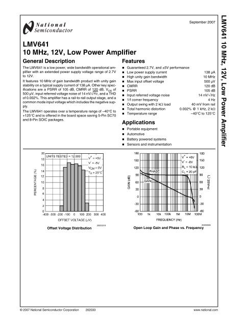
Offset Voltage Distribution<br />
20203319<br />
20203326<br />
Open Loop Gain and Phase vs. Frequency<br />
© 2007 National Semiconductor Corporation 202033 www.national.com
<strong>LMV641</strong><br />
Absolute Maximum Ratings (Note 1)<br />
If Military/Aerospace specified devices are required,<br />
please contact the National Semiconductor Sales Office/<br />
Distributors for availability and specifications.<br />
ESD Tolerance (Note 2)<br />
Human Body Model<br />
2000V<br />
Machine Model<br />
200V<br />
Differential Input V ID<br />
±0.3V<br />
Supply Voltage (V S = V + - V − ) 13.2V<br />
Input/Output Pin Voltage<br />
V + +0.3V, V − −0.3V<br />
Storage Temperature Range<br />
−65°C to +150°C<br />
2.7V DC Electrical Characteristics<br />
Junction Temperature (Note 3)<br />
Soldering Information<br />
+150°C<br />
Infrared or Convection (20 sec) 235°C<br />
Wave Soldering Lead Temp (<strong>10</strong> sec) 260°C<br />
Operating Ratings (Note 1)<br />
Temperature Range (Note 3) −40°C to 125°C<br />
Supply Voltage (V S = V + - V − )<br />
2.7V to <strong>12V</strong><br />
Package Thermal Resistance (θ JA )(Note 3)<br />
5-Pin SC70<br />
8-Pin SOIC<br />
Unless otherwise specified, all limits are guaranteed for T A = 25°C, V + = 2.7V, V − = 0V, V O = V CM = V + /2, and R L > 1 MΩ.<br />
Boldface limits apply at the temperature extremes.<br />
Symbol Parameter Conditions Min<br />
(Note 5)<br />
Typ<br />
(Note 4)<br />
Max<br />
(Note 5)<br />
V OS Input Offset Voltage 30 500<br />
750<br />
456°C/W<br />
166°C/W<br />
TC V OS Input Offset Average Drift 0.1 μV/°C<br />
I B Input Bias Current (Note 6) 75 95<br />
1<strong>10</strong><br />
I OS Input Offset Current 0.9 5 nA<br />
CMRR Common Mode Rejection Ratio 0V ≤ V CM ≤ 1.7V 89<br />
84<br />
PSRR <strong>Power</strong> Supply Rejection Ratio 2.7V ≤ V + ≤ <strong>10</strong>V, V CM = 0.5 94.5<br />
92.5<br />
CMVR<br />
Input Common-Mode Voltage<br />
Range<br />
2.7V ≤ V + ≤ <strong>12V</strong>, V CM = 0.5 94<br />
92<br />
CMRR ≥ 80 dB<br />
CMRR ≥ 68 dB<br />
A VOL Large Signal Voltage Gain 0.3V ≤ V O ≤ 2.4V, R L = 2 kΩ to V + /2<br />
0.4V ≤ V O ≤ 2.3V, R L = 2 kΩ to V + /2<br />
0.3V ≤ V O ≤ 2.4V, R L = <strong>10</strong> kΩ to V + /2<br />
0.4V ≤ V O ≤ 2.3V, R L = <strong>10</strong> kΩ to V + /2<br />
114<br />
<strong>10</strong>5<br />
<strong>10</strong>0<br />
Units<br />
µV<br />
nA<br />
dB<br />
dB<br />
0 1.8 V<br />
V O Output Swing High R L = 2 kΩ to V + /2, V IN = <strong>10</strong>0 mV 42 58<br />
68<br />
I OUT<br />
R L = <strong>10</strong> kΩ to V + /2, V IN = <strong>10</strong>0 mV 22 35<br />
40<br />
Output Swing <strong>Low</strong> R L = 2 kΩ to V + /2, V IN = <strong>10</strong>0 mV 38 48<br />
58<br />
Sourcing and Sinking Output<br />
Current<br />
R L = <strong>10</strong> kΩ to V + /2, V IN = <strong>10</strong>0 mV 18 30<br />
35<br />
V IN_DIFF = <strong>10</strong>0 mV to<br />
V O = V + /2 (Note 7)<br />
82<br />
78<br />
86<br />
82<br />
88<br />
98<br />
Sourcing 22<br />
Sinking 25<br />
I S Supply Current 138 170<br />
220<br />
SR Slew Rate A V = +1, V O = 1 V PP Rising (<strong>10</strong>% to 90%) 2.3<br />
Falling (90% to <strong>10</strong>%) 1.6<br />
dB<br />
mV from<br />
rail<br />
GBW Gain Bandwidth Product <strong>10</strong> <strong>MHz</strong><br />
e n Input-Referred Voltage Noise f = 1 kHz 14 nV/<br />
mA<br />
μA<br />
V/μs<br />
www.national.com 2
Symbol Parameter Conditions Min<br />
(Note 5)<br />
Typ<br />
(Note 4)<br />
Max<br />
(Note 5)<br />
i n Input-Referred Current Noise f = 1 kHz 0.15 pA/<br />
THD Total Harmonic Distortion f = 1 kHz, A V = 2, R L = 2 kΩ 0.014 %<br />
Units<br />
<strong>LMV641</strong><br />
<strong>10</strong>V DC Electrical Characteristics<br />
Unless otherwise specified, all limits are guaranteed for T A = 25°C, V + = <strong>10</strong>V, V − = 0V,V O = V CM = V + /2, and R L > 1 MΩ. Boldface<br />
limits apply at the temperature extremes.<br />
Symbol Parameter Conditions Min<br />
(Note 5)<br />
Typ<br />
(Note 4)<br />
Max<br />
(Note 5)<br />
V OS Input Offset Voltage 5 500<br />
750<br />
TC V OS Input Offset Average Drift 0.1 μV/°C<br />
I B Input Bias Current (Note 6) 70 90<br />
<strong>10</strong>5<br />
I OS Input Offset Current 0.7 5 nA<br />
CMRR Common Mode Rejection Ratio 0V ≤ V CM ≤ 9V 94<br />
90<br />
PSRR <strong>Power</strong> Supply Rejection Ratio 2.7V ≤ V + ≤ <strong>10</strong>V, V CM = 0.5V 94.5<br />
92.5<br />
CMVR<br />
Input Common-Mode Voltage<br />
Range<br />
2.7V ≤ V + ≤ <strong>12V</strong>, V CM = 0.5V 94<br />
92<br />
CMRR ≥ 80 dB<br />
CMRR ≥ 76 dB<br />
A VOL Large Signal Voltage Gain 0.3V ≤ V O ≤ 9.7V, R L = 2 kΩ to V + /2<br />
I OUT<br />
0.4V ≤ V O ≤ 9.6V, R L = 2 kΩ to V + /2<br />
0.3V ≤ V O ≤ 9.7V, R L = <strong>10</strong> kΩ to V + /2<br />
0.4V ≤ V O ≤ 9.6V, R L = <strong>10</strong> kΩ to V + /2<br />
120<br />
<strong>10</strong>5<br />
<strong>10</strong>0<br />
Units<br />
µV<br />
nA<br />
dB<br />
dB<br />
0 9.1 V<br />
V O Output Swing High R L = 2 kΩ to V + /2, V IN = <strong>10</strong>0 mV 68 95<br />
125<br />
90<br />
85<br />
97<br />
92<br />
99<br />
<strong>10</strong>4<br />
R L = <strong>10</strong> kΩ to V + /2, V IN = <strong>10</strong>0 mV 37 55<br />
65<br />
Output Swing <strong>Low</strong> R L = 2 kΩ to V + /2, V IN = <strong>10</strong>0 mV 65 90<br />
1<strong>10</strong><br />
Sourcing and Sinking Output<br />
Current<br />
R L = <strong>10</strong> kΩ to V + /2, V IN = <strong>10</strong>0 mV 32 42<br />
52<br />
V IN_DIFF = <strong>10</strong>0 mV<br />
to V O = V + /2 (Note 7)<br />
Sourcing 26<br />
Sinking 112<br />
I S Supply Current 158 190<br />
240<br />
SR Slew Rate A V = +1, V O = 2V to 8 Rising (<strong>10</strong>% to 90%) 2.6<br />
V PP Falling (90% to <strong>10</strong>%) 1.6<br />
dB<br />
mV from<br />
rail<br />
GBW Gain Bandwidth Product <strong>10</strong> <strong>MHz</strong><br />
e n Input-Referred Voltage Noise f = 1 kHz 14 nV/<br />
i n Input-Referred Current Noise f = 1 kHz 0.15 pA/<br />
THD Total Harmonic Distortion f = 1 kHz, A V = 2, R L = 2 kΩ 0.002 %<br />
mA<br />
μA<br />
V/μs<br />
3 www.national.com
<strong>LMV641</strong><br />
Note 1: Absolute Maximum Ratings indicate limits beyond which damage to the device may occur. Operating Ratings indicate conditions for which the device is<br />
intended to be functional, but specific performance is not guaranteed. For guaranteed specifications and the test conditions, see the Electrical Characteristics<br />
Tables.<br />
Note 2: Human Body Model, applicable std. MIL-STD-883, Method 3015.7. Machine Model, applicable std. JESD22-A115-A (ESD MM std. of JEDEC)<br />
Field-Induced Charge-Device Model, applicable std. JESD22-C<strong>10</strong>1-C (ESD FICDM std. of JEDEC).<br />
Note 3: The maximum power dissipation is a function of T J(MAX , θ JA . The maximum allowable power dissipation at any ambient temperature is<br />
P D = (T J(MAX) - T A )/ θ JA . All numbers apply for packages soldered directly onto a PC board.<br />
Note 4: Typical values represent the most likely parametric norm as determined at the time of characterization. Actual typical values may vary over time and will<br />
also depend on the application and configuration. The typical values are not tested and are not guaranteed on shipped production material.<br />
Note 5: Limits are <strong>10</strong>0% production tested at 25°C. Limits over the operating temperature range are guaranteed through correlations using Statistical Quality<br />
Control (SQC) method.<br />
Note 6: Positive current corresponds to current flowing into the device.<br />
Note 7: The part is not short circuit protected and is not recommended for operation with low resistive loads. Typical sourcing and sinking output current curves<br />
are provided in the Typical Performance Characteristics and should be consulted before designing for heavy loads.<br />
Connection Diagrams<br />
5-Pin SC70<br />
8-Pin SOIC<br />
Top View<br />
20203339<br />
Top View<br />
20203340<br />
Ordering Information<br />
Package Part Number Package Marking Transport Media NSC Drawing<br />
5-Pin SC70<br />
<strong>LMV641</strong>MG<br />
<strong>LMV641</strong>MGE<br />
A99<br />
1k Units Tape and Reel<br />
250 Units Tape and Reel<br />
MAA05A<br />
<strong>LMV641</strong>MGX<br />
3k Units Tape and Reel<br />
8-Pin SOIC<br />
<strong>LMV641</strong>MA<br />
<strong>LMV641</strong>MAE<br />
<strong>LMV641</strong>MA<br />
95 Units/Rail<br />
250 Units Tape and Reel<br />
M08A<br />
<strong>LMV641</strong>MAX<br />
2.5k Tape and Reel<br />
www.national.com 4
Typical Performance Characteristics Unless otherwise specified, T A = 25°C, V + = <strong>10</strong>V, V − = 0V,<br />
V CM = V S /2.<br />
<strong>LMV641</strong><br />
Supply Current vs. Supply Voltage<br />
Offset Voltage vs. Supply Voltage<br />
20203307<br />
20203308<br />
Offset Voltage vs. V CM<br />
20203309<br />
Offset Voltage vs. V CM<br />
202033<strong>10</strong><br />
Offset Voltage vs. V CM<br />
20203311<br />
Offset Voltage vs. V CM<br />
20203312<br />
5 www.national.com
<strong>LMV641</strong><br />
Offset Voltage Distribution<br />
Offset Voltage Distribution<br />
20203321<br />
20203319<br />
CMRR vs. Frequency<br />
PSRR vs. Frequency<br />
20203366<br />
20203367<br />
Input Bias Current vs. V CM<br />
20203317<br />
Input Bias Current vs. V CM<br />
20203318<br />
www.national.com 6
Open Loop Gain and Phase with Capacitive Load<br />
Open Loop Gain and Phase with Capacitive Load<br />
<strong>LMV641</strong><br />
20203327<br />
20203328<br />
Open Loop Gain and Phase with Resistive Load<br />
Open Loop Gain and Phase with Supply Voltage<br />
20203329<br />
20203330<br />
Input Referred Noise Voltage vs. Frequency<br />
Close Loop Output Impedance vs. Frequency<br />
20203325<br />
20203335<br />
7 www.national.com
<strong>LMV641</strong><br />
THD+N vs. Frequency<br />
THD+N vs. Frequency<br />
20203368<br />
20203369<br />
THD+N vs. V OUT<br />
20203370<br />
THD+N vs. V OUT<br />
20203371<br />
Sourcing Current vs. Supply Voltage<br />
Sinking Current vs. Supply Voltage<br />
20203334<br />
20203365<br />
www.national.com 8
<strong>LMV641</strong><br />
Sourcing Current vs. V OUT<br />
20203331<br />
Sinking Current vs. V OUT<br />
20203332<br />
Sourcing Current vs. V OUT<br />
20203333<br />
Large Signal Transient<br />
20203324<br />
Small Signal Transient Response<br />
Small Signal Transient Response<br />
20203322<br />
20203323<br />
9 www.national.com
<strong>LMV641</strong><br />
Output Swing High vs. Supply Voltage<br />
Output Swing <strong>Low</strong> vs. Supply voltage<br />
20203313<br />
20203314<br />
Output Swing High vs. Supply Voltage<br />
Output Swing <strong>Low</strong> and Supply Voltage<br />
20203315<br />
20203316<br />
Slew Rate vs. Supply Voltage<br />
20203372<br />
www.national.com <strong>10</strong>
Application Information<br />
ADVANTAGES OF THE <strong>LMV641</strong><br />
<strong>LMV641</strong><br />
<strong>Low</strong> Voltage and <strong>Low</strong> <strong>Power</strong> Operation<br />
The <strong>LMV641</strong> has performance guaranteed at supply voltages<br />
of 2.7V and <strong>10</strong>V. It is guaranteed to be operational at all supply<br />
voltages between 2.7V and 12.0V. The <strong>LMV641</strong> draws a<br />
low supply current of 138 µA. The <strong>LMV641</strong> provides the low<br />
voltage and low power amplification which is essential for<br />
portable applications.<br />
Wide Bandwidth<br />
Despite drawing the very low supply current of 138 µA, the<br />
<strong>LMV641</strong> manages to provide a wide unity gain bandwidth of<br />
<strong>10</strong> <strong>MHz</strong>. This is easily one of the best bandwidth to power<br />
ratios ever achieved, and allows this op amp to provide wideband<br />
amplification while using the minimum amount of power.<br />
This makes the <strong>LMV641</strong> ideal for low power signal processing<br />
applications such as portable media players and other accessories.<br />
<strong>Low</strong> Input Referred Noise<br />
The <strong>LMV641</strong> provides a flatband input referred voltage noise<br />
density of 14 nV/ , which is significantly better than the<br />
noise performance expected from a low power op amp. This<br />
op amp also feature exceptionally low 1/f noise, with a very<br />
low 1/f noise corner frequency of 4 Hz. Because of this the<br />
<strong>LMV641</strong> is ideal for low power applications which require decent<br />
noise performance, such as PDAs and portable sensors.<br />
Ground Sensing and Rail-to-Rail Output<br />
The <strong>LMV641</strong> has a rail-to-rail output stage, which provides<br />
the maximum possible output dynamic range. This is especially<br />
important for applications requiring a large output swing.<br />
The input common mode range of this part includes the negative<br />
supply rail which allows direct sensing at ground in a<br />
single supply operation.<br />
Small Size<br />
The small footprint of the packages for the <strong>LMV641</strong> saves<br />
space on printed circuit boards, and enables the design of<br />
smaller and more compact electronic products. Long traces<br />
between the signal source and the op amp make the signal<br />
path susceptible to noise. By using a physically smaller package,<br />
these op amps can be placed closer to the signal source,<br />
reducing noise pickup and enhancing signal integrity.<br />
FIGURE 1. Gain vs. Frequency for an Op Amp<br />
20203359<br />
An op amp, ideally, has a dominant pole close to DC which<br />
causes its gain to decay at the rate of 20 dB/decade with respect<br />
to frequency. If this rate of decay, also known as the<br />
rate of closure (ROC), remains the same until the op amp's<br />
unity gain bandwidth, then the op amp is stable. If, however,<br />
a large capacitance is added to the output of the op amp, it<br />
combines with the output impedance of the op amp to create<br />
another pole in its frequency response before its unity gain<br />
frequency (Figure 1). This increases the ROC to 40 dB/<br />
decade and causes instability.<br />
In such a case, a number of techniques can be used to restore<br />
stability to the circuit. The idea behind all these schemes is to<br />
modify the frequency response such that it can be restored to<br />
an ROC of 20 dB/decade, which ensures stability.<br />
In The Loop Compensation<br />
Figure 2 illustrates a compensation technique, known as in<br />
the loop compensation, that employs an RC feedback circuit<br />
within the feedback loop to stabilize a non-inverting amplifier<br />
configuration. A small series resistance, R S , is used to isolate<br />
the amplifier output from the load capacitance, C L , and a small<br />
capacitance, C F , is inserted across the feedback resistor to<br />
bypass C L at higher frequencies.<br />
STABILITY OF OP AMP CIRCUITS<br />
If the phase margin of the <strong>LMV641</strong> is plotted with respect to<br />
the capacitive load (C L ) at its output, and if C L is increased<br />
beyond <strong>10</strong>0 pF then the phase margin reduces significantly.<br />
This is because the op amp is designed to provide the maximum<br />
bandwidth possible for a low supply current. Stabilizing<br />
the <strong>LMV641</strong> for higher capacitive loads would have required<br />
either a drastic increase in supply current, or a large internal<br />
compensation capacitance, which would have reduced the<br />
bandwidth. Hence, if this device is to be used for driving higher<br />
capacitive loads, it will have to be externally compensated.<br />
20203358<br />
FIGURE 2. In the Loop Compensation<br />
11 www.national.com
<strong>LMV641</strong><br />
The values for R S and C F are decided by ensuring that the<br />
zero attributed to C F lies at the same frequency as the pole<br />
attributed to C L . This ensures that the effect of the second<br />
pole on the transfer function is compensated for by the presence<br />
of the zero, and that the ROC is maintained at 20 dB/<br />
decade. For the circuit shown in Figure 2 the values of R S and<br />
C F are given by Equation 1. Values of R S and C F required for<br />
maintaining stability for different values of C L , as well as the<br />
phase margins obtained, are shown in Table 1. R F and R IN<br />
are <strong>10</strong> kΩ, R L is 2 kΩ, while R OUT is 680Ω.<br />
TABLE 1.<br />
C L (nF) R S (Ω) C F (pF) Phase Margin (°)<br />
0.5 680 <strong>10</strong> 17.4<br />
1 680 20 12.4<br />
1.5 680 30 <strong>10</strong>.1<br />
The <strong>LMV641</strong> is capable of driving heavy capacitive loads of<br />
up to 1 nF without oscillating, however it is recommended to<br />
use compensation should the load exceed 1 nF. Using this<br />
methodology will reduce any excessive ringing and help<br />
maintain the phase margin for stability. The values of the<br />
compensation network tabulated above illustrate the phase<br />
margin degradation as a function of the capacitive load.<br />
Typical Applications<br />
ANISOTROPIC MAGNETORESISTIVE SENSOR<br />
The low operating current of the <strong>LMV641</strong> makes it a good<br />
choice for battery operated applications. Figure 4 shows two<br />
<strong>LMV641</strong>s in a portable application with a magnetic field sensor.<br />
The <strong>LMV641</strong>s condition the output from an anisotropic<br />
(1)<br />
Although this methodology provides circuit stability for any<br />
load capacitance, it does so at the price of bandwidth. The<br />
closed loop bandwidth of the circuit is now limited by R F and<br />
C F .<br />
Compensation by External Resistor<br />
In some applications it is essential to drive a capacitive load<br />
without sacrificing bandwidth. In such a case, in the loop compensation<br />
is not viable. A simpler scheme for compensation<br />
is shown in Figure 3. A resistor, R ISO , is placed in series between<br />
the load capacitance and the output. This introduces a<br />
zero in the circuit transfer function, which counteracts the effect<br />
of the pole formed by the load capacitance, and ensures<br />
stability. The value of R ISO to be used should be decided depending<br />
on the size of C L and the level of performance desired.<br />
Values ranging from 5Ω to 50Ω are usually sufficient to<br />
ensure stability. A larger value of R ISO will result in a system<br />
with less ringing and overshoot, but will also limit the output<br />
swing and the short circuit current of the circuit.<br />
20203360<br />
FIGURE 3. Compensation by Isolation Resistor<br />
magnetoresistive (AMR) sensor. The sensor is arranged in<br />
the form of a Wheatstone bridge. This type of sensor can be<br />
used to accurately measure the current (either DC or AC)<br />
flowing in a wire by measuring the magnetic flux density, B,<br />
emanating from the wire.<br />
20203341<br />
FIGURE 4. A Battery Operated System for Contact-Less Current Sensing Using an Anisotropic Magnetoresistive Sensor<br />
www.national.com 12
In this circuit, the use of a 9-volt alkaline battery exploits the<br />
<strong>LMV641</strong>’s high voltage and low supply current for a low power,<br />
portable current sensing application. The sensor converts<br />
an incident magnetic field (via the magnetic flux linkage) in<br />
the sensitive direction, to a balanced voltage output. The<br />
<strong>LMV641</strong> can be utilized for moderate to high current sensing<br />
applications (from a few milliamps and up to 20A) using a<br />
nearby external conductor providing the sensed magnetic<br />
field to the bridge. The circuit shows a Honeywell HMC<strong>10</strong>51Z<br />
used as a current sensor. Note that the circuit must be calibrated<br />
based on the final displacement of the sensed conductor<br />
relative to the measurement bridge. Typically, once the<br />
sensor has been oriented properly, with respect to the conductor<br />
to be measured, the conductor can be placed about<br />
one centimeter away from the bridge and have reasonable<br />
capability of measuring from tens of milliamperes to beyond<br />
20 amperes.<br />
In Figure 4, U1 is configured as a single differential input amplifier.<br />
Its input impedance is relatively low, however, and<br />
requires that the source impedance of the sensor be considered<br />
in the gain calculations. Also, the asymmetrical loading<br />
on the bridge will produce a small offset voltage that can be<br />
cancelled out with the offset trim circuit shown in Figure 4.<br />
Figure 5 shows a typical magnetoresistive Wheatstone bridge<br />
and the Thevenin equivalent of its resistive elements. As we<br />
shall see, the Thevenin equivalent model of the sensor is<br />
useful in calculating the gain needed in the differential amplifier.<br />
Using Thevenin’s Theorem, the bridge can be reduced to two<br />
voltage sources with series resistances. ΔR is normally very<br />
small in comparison to R, thus the Thevenin equivalent resistance,<br />
commonly called the source resistance, can be<br />
taken to be R. When a bias voltage is applied between V EXC<br />
and ground, in the absence of a magnetic field, all of the resistances<br />
are considered equal. The voltage at Sig+ and Sig<br />
− is half V EXC , or 4.5V, and Sig+ - Sig− = 0. Bridges are designed<br />
such that, when immersed in a magnetic field, opposite<br />
resistances in the bridge change by ±ΔR with an amount<br />
proportional to the strength of the magnetic field. This causes<br />
the bridge's output differential voltage, to change from its half<br />
V EXC value. Thus Sig+ - Sig− = Vsig ≠ 0. With four active<br />
elements, the output voltage is:<br />
Since ΔR is proportional to the field strength, B S , the amount<br />
of output voltage from the sensor is a function of sensor sensitivity,<br />
S. This expression can rewritten as<br />
V SIG = V EXC · S · B S , where<br />
S = material constant (nominally 1 mV/V/gauss)<br />
B S = magnetic flux in gauss<br />
A simplified schematic of a single op amp, differential amplifier<br />
is shown in Figure 6. The Thevenin equivalent circuit of<br />
the sensor can be used to calculate the gain of this amplifier.<br />
<strong>LMV641</strong><br />
20203342<br />
FIGURE 6. Differential Input <strong>Amplifier</strong><br />
20203344<br />
The Honeywell HMC<strong>10</strong>51Z AMR sensor has nominal 1 kΩ<br />
elements and a sensitivity of 1 mV/V/gauss and is being used<br />
with 9V of excitation with a full scale magnetic field range of<br />
±6 gauss. At full-scale, the resistors will have ΔR ≈ 12Ω and<br />
<strong>10</strong>8 mV will be seen from Sig− to Sig+ (refer to Figure 7).<br />
20203343<br />
FIGURE 5. Anisotropic Magnetoresistive Wheatstone<br />
Bridge Sensor, (a), and Thevenin Equivalent Circuit, (b)<br />
13 www.national.com
<strong>LMV641</strong><br />
FIGURE 7. Sensor Output with No Load<br />
20203346<br />
performs a temperature compensation function for the bridge<br />
so that it will have greater accuracy over a wide range of operational<br />
temperatures. With mangetoresistive sensors, temperature<br />
drift of the bridge sensitivity is negative and linear,<br />
and in the case of the sensor used here, is nominally −3000<br />
PP/M. Thus the gain of U2 needs to increase proportionally<br />
with increasing temperature, suggesting a thermistor with a<br />
positive temperature coefficient. Selection of the temperature<br />
compensation resistor, R TH , depends on the additional gain<br />
required, on the thermistor chosen, and is dependent on the<br />
thermistor’s %/°C shift in resistance. For best op amp compatibility,<br />
the thermistor resistance should be greater than<br />
<strong>10</strong>00Ω. R TH should also be much less than R A , the feedback<br />
resistor. Because the temperature coefficient of the AMR<br />
bridge is largely linear, R TH also needs to behave in a linear<br />
fashion with temperature, thus R A is placed in parallel with<br />
R TH , which acts to linearize the thermistor.<br />
Referring to the simplified diagram in Figure 6, and assuming<br />
that required full scale at the output of the amplifier is 2.5V, a<br />
gain of 23.2 is needed for U1. It is clear from the Thevenin<br />
equivalent circuit in Figure 8 that a sensor Thevenin equivalent<br />
source resistance, R THEV , of 500Ω will be in series with<br />
both the inverting and non-inverting inputs of the <strong>LMV641</strong>.<br />
Therefore, the required gain is:<br />
Choosing R 1 = R 2 = 24.5 kΩ, then R 4 will be approximately<br />
580 kΩ. The actual values chosen will depend on the fullscale<br />
needs of the succeeding circuitry as well as bandwidth<br />
requirements. The values shown here provide a −3 dB bandwidth<br />
of approximately 431 kHz, and are found as follows.<br />
Gain Error and Bandwidth Consideration if Using an<br />
Analog to Digital Converter<br />
The bandwidth available from Figure 4 is dependent on the<br />
system closed loop gain required and the maximum gain-error<br />
allowed if driving an analog to digital converter (ADC). If<br />
the output from the sensor is intended to drive an ADC, the<br />
bandwidth will be considerably reduced from the closed-loop<br />
corner frequency. This is because the gain error of the preamplifier<br />
stage needs to be taken into account when calculating<br />
total error budget. Good practice dictates that the gain<br />
error of the amplifier be less than or equal to half LSB (preferably<br />
less in order to allow for other system errors that will eat<br />
up a portion of the available error budget) of the ADC. However,<br />
at the −3 dB corner frequency the gain error for any<br />
amplifier is 29.3%. In reality, the gain starts rolling off long<br />
before the −3 dB corner is reached. For example, if the amplifier<br />
is driving an 8-bit ADC, the minimum gain error allowed<br />
for half LSB would be approximately 0.2%. To achieve this<br />
gain error with the op amp, the maximum frequency of interest<br />
can be no higher than<br />
where n is the bit resolution of the ADC and f −3 dB is the closed<br />
loop corner frequency.<br />
Given that the <strong>LMV641</strong> has a GBW of <strong>10</strong> <strong>MHz</strong>, and is operating<br />
with a closed loop gain of 26.3, its closed loop bandwidth<br />
is 380 kHZ, therefore<br />
20203347<br />
FIGURE 8. Thevenin Equivalent Showing Required Gain<br />
By choosing input resistor values for R 1 and R 2 that are four<br />
to ten times the bridge element resistance, the bridge is minimally<br />
loaded and the offset errors induced by the op amp<br />
stages are minimized. These resistors should have 1% tolerance,<br />
or better, for the best noise rejection and offset minimization.<br />
Referring once again to Figure 4, U2 is an additional gain<br />
stage with a thermistor element, R TH , in the feedback loop. It<br />
which is the highest frequency that can be measured with required<br />
accuracy.<br />
www.national.com 14
VOICEBAND FILTER<br />
The majority of the energy of recognizable speech is within a<br />
band of frequencies between 200 Hz and 4 kHz. Therefore it<br />
is beneficial to design circuits which transmit telephone signals<br />
that pass only certain frequencies and eliminate unwanted<br />
signals (noise) that could interfere with conversations and<br />
introduce error into control signals. The pass band of these<br />
circuits is defined as the ranges of frequencies that are<br />
passed. A telephone system voice frequency (VF) channel<br />
has a pass band of 0 Hz to 4 kHz. Specifically for human<br />
voices most of the energy content is found from 300 Hz to 3<br />
kHz and any signal within this range is considered an in-band<br />
signal. Alternatively, any signal outside this range but within<br />
the VF channel is considered an out-of-band signal.<br />
To properly recover a voice signal in applications such as<br />
cellular phones, cordless phones, and voice pagers, a low<br />
power bandpass filter that is matched to the human voice<br />
spectrum can be implemented using an <strong>LMV641</strong> op amp.<br />
Figure 9 shows a multi-feedback, multi-pole filter (2 nd order<br />
response) with a gain of −1. The lower 3 dB cutoff frequency<br />
which is set by the DC blocking capacitor C 1 and resistor R 1<br />
is 60 Hz and the upper cutoff frequency is 3.5 kHz.<br />
The total current consumption is a mere 138 µA. The LV641<br />
is operating with a gain of −1, but the circuit is easily modified<br />
to add gain. The op amp is powered from a single supply,<br />
hence the need for offset (common-mode) adjustment of its<br />
output, which is set to ½ V S via its non-inverting input.<br />
This filter is also useful in applications for battery operated<br />
talking toys and games.<br />
20203373<br />
FIGURE 9. <strong>Low</strong> <strong>Power</strong> Voice In-Band Receive Filter for<br />
Battery-<strong>Power</strong>ed Portable Use<br />
<strong>LMV641</strong><br />
15 www.national.com
<strong>LMV641</strong><br />
Physical Dimensions inches (millimeters) unless otherwise noted<br />
5-Pin SC70<br />
NS Package Number MAA05A<br />
8-Pin SOIC<br />
NS Package Number M08A<br />
www.national.com 16
<strong>Notes</strong><br />
<strong>LMV641</strong><br />
17 www.national.com
<strong>LMV641</strong> <strong>10</strong> <strong>MHz</strong>, <strong>12V</strong>, <strong>Low</strong> <strong>Power</strong> <strong>Amplifier</strong><br />
<strong>Notes</strong><br />
THE CONTENTS OF THIS DOCUMENT ARE PROVIDED IN CONNECTION WITH NATIONAL SEMICONDUCTOR CORPORATION<br />
(“NATIONAL”) PRODUCTS. NATIONAL MAKES NO REPRESENTATIONS OR WARRANTIES WITH RESPECT TO THE ACCURACY<br />
OR COMPLETENESS OF THE CONTENTS OF THIS PUBLICATION AND RESERVES THE RIGHT TO MAKE CHANGES TO<br />
SPECIFICATIONS AND PRODUCT DESCRIPTIONS AT ANY TIME WITHOUT NOTICE. NO LICENSE, WHETHER EXPRESS,<br />
IMPLIED, ARISING BY ESTOPPEL OR OTHERWISE, TO ANY INTELLECTUAL PROPERTY RIGHTS IS GRANTED BY THIS<br />
DOCUMENT.<br />
TESTING AND OTHER QUALITY CONTROLS ARE USED TO THE EXTENT NATIONAL DEEMS NECESSARY TO SUPPORT<br />
NATIONAL’S PRODUCT WARRANTY. EXCEPT WHERE MANDATED BY GOVERNMENT REQUIREMENTS, TESTING OF ALL<br />
PARAMETERS OF EACH PRODUCT IS NOT NECESSARILY PERFORMED. NATIONAL ASSUMES NO LIABILITY FOR<br />
APPLICATIONS ASSISTANCE OR BUYER PRODUCT DESIGN. BUYERS ARE RESPONSIBLE FOR THEIR PRODUCTS AND<br />
APPLICATIONS USING NATIONAL COMPONENTS. PRIOR TO USING OR DISTRIBUTING ANY PRODUCTS THAT INCLUDE<br />
NATIONAL COMPONENTS, BUYERS SHOULD PROVIDE ADEQUATE DESIGN, TESTING AND OPERATING SAFEGUARDS.<br />
EXCEPT AS PROVIDED IN NATIONAL’S TERMS AND CONDITIONS OF SALE FOR SUCH PRODUCTS, NATIONAL ASSUMES NO<br />
LIABILITY WHATSOEVER, AND NATIONAL DISCLAIMS ANY EXPRESS OR IMPLIED WARRANTY RELATING TO THE SALE<br />
AND/OR USE OF NATIONAL PRODUCTS INCLUDING LIABILITY OR WARRANTIES RELATING TO FITNESS FOR A PARTICULAR<br />
PURPOSE, MERCHANTABILITY, OR INFRINGEMENT OF ANY PATENT, COPYRIGHT OR OTHER INTELLECTUAL PROPERTY<br />
RIGHT.<br />
LIFE SUPPORT POLICY<br />
NATIONAL’S PRODUCTS ARE NOT AUTHORIZED FOR USE AS CRITICAL COMPONENTS IN LIFE SUPPORT DEVICES OR<br />
SYSTEMS WITHOUT THE EXPRESS PRIOR WRITTEN APPROVAL OF THE CHIEF EXECUTIVE OFFICER AND GENERAL<br />
COUNSEL OF NATIONAL SEMICONDUCTOR CORPORATION. As used herein:<br />
Life support devices or systems are devices which (a) are intended for surgical implant into the body, or (b) support or sustain life and<br />
whose failure to perform when properly used in accordance with instructions for use provided in the labeling can be reasonably expected<br />
to result in a significant injury to the user. A critical component is any component in a life support device or system whose failure to perform<br />
can be reasonably expected to cause the failure of the life support device or system or to affect its safety or effectiveness.<br />
National Semiconductor and the National Semiconductor logo are registered trademarks of National Semiconductor Corporation. All other<br />
brand or product names may be trademarks or registered trademarks of their respective holders.<br />
Copyright© 2007 National Semiconductor Corporation<br />
For the most current product information visit us at www.national.com<br />
National Semiconductor<br />
Americas Customer<br />
Support Center<br />
Email:<br />
new.feedback@nsc.com<br />
Tel: 1-800-272-9959<br />
National Semiconductor Europe<br />
Customer Support Center<br />
Fax: +49 (0) 180-530-85-86<br />
Email: europe.support@nsc.com<br />
Deutsch Tel: +49 (0) 69 9508 6208<br />
English Tel: +49 (0) 870 24 0 2171<br />
Français Tel: +33 (0) 1 41 91 8790<br />
National Semiconductor Asia<br />
Pacific Customer Support Center<br />
Email: ap.support@nsc.com<br />
National Semiconductor Japan<br />
Customer Support Center<br />
Fax: 81-3-5639-7507<br />
Email: jpn.feedback@nsc.com<br />
Tel: 81-3-5639-7560<br />
www.national.com