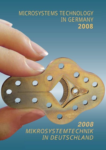
MICROSYSTEMS TECHNOLOGY IN GERMANY - AHK
MICROSYSTEMS TECHNOLOGY IN GERMANY - AHK
MICROSYSTEMS TECHNOLOGY IN GERMANY - AHK

Create successful ePaper yourself
Turn your PDF publications into a flip-book with our unique Google optimized e-Paper software.
<strong>MICROSYSTEMS</strong> <strong>TECHNOLOGY</strong><br />
<strong>IN</strong> <strong>GERMANY</strong><br />
2008<br />
2008<br />
MIKROSYSTEMTECHNIK<br />
<strong>IN</strong> DEUTSCHLAND
Table of Contents<br />
4<br />
6 Welcoming Address<br />
Grußwort<br />
Dr. Annette Schavan<br />
Federal Minister for Education and Research<br />
Bundesministerin für Bildung und Forschung<br />
8 Positioning in International<br />
Competition<br />
Zur Positionierung im<br />
internationalen Wettbewerb<br />
10 VDE-GMM: Microsystems Technology Drives<br />
Innovation in Leading Markets<br />
Mikrosystemtechnik – Innovationstreiber<br />
für Leitmärkte<br />
13 Contributions to<br />
Topical Fields of Innovation<br />
Beiträge zu aktuellen<br />
Innovationsfeldern<br />
14 Helmut Seidel, Universität des Saarlandes:<br />
Microactuators<br />
16 Peter Woias, IMTEK:<br />
MicroEnergy Harvesting – Energy Supply for distributed<br />
embedded Microsystems<br />
18 Jürgen Mohr, Forschungszentrum Karlsruhe:<br />
Micro-Optics<br />
20 OSRAM Opto Semiconductors:<br />
High Brightness LEDs for Light Engines<br />
22 Thomas Stieglitz, IMTEK:<br />
Intelligent Implants<br />
24 Johannes Dehm, DGBMT im VDE:<br />
Latest Results and Solutions in Preventive<br />
Micromedicine<br />
26 Reiner Wichert, Fraunhofer-Verbund Mikroelektronik:<br />
The Fraunhofer Alliance „Ambient Assisted Living“<br />
28 Katrin Gaßner, VDI/VDE-IT:<br />
Smart Labels for Logistic Applications<br />
30 Hartmut Strese, VDI/VDE-IT:<br />
Intelligent Technical Textiles<br />
32 Herbert Reichl, Fraunhofer IZM, at al:<br />
More than Moore, Hetero System Integration<br />
and Smart System Integration –<br />
Three Approaches – one Goal: Smarter Products<br />
and Processes<br />
38 The 2 nd German Congress<br />
on Microsystem Technologies<br />
2007<br />
Der 2. Deutsche Mikrosystemtechnik-Kongress<br />
2007<br />
40 Thomas Gessner, TU Chemnitz:<br />
Review of the 2 nd German Congress on<br />
Microsystem Technologies<br />
42 Roland Zengerle, IMTEK, et al:<br />
Microfl uidic Platforms for Miniaturization, Integration<br />
and Automation of Biochemical Assays<br />
44 Christian Voss, Jörg Müller, TU Hamburg-Harburg:<br />
A Mechanical Microsystem for Restoration of<br />
Spinal Cord Continuity after Paraplegia<br />
46 Kathrin Knese, Robert Bosch GmbH, et al:<br />
Novel Surface Micromachining Technology<br />
for Fabrication of Capacitive Pressure Sensors<br />
Based on Porous Silicon<br />
48 Thomas Otto, Ray Saupe, Fraunhofer IZM, et al:<br />
Forensic Investigation Using MEMS-Spectrometers<br />
50 Anna Gerken, Johannes Paul, Sensitec GmbH:<br />
Use of the Tunnelmagnetoresistive Effect for Sensor<br />
Applications<br />
52 Katrin Müller, Motorola GmbH:<br />
Nutriwear – Nutrition Management Using Smart Textiles
54 Jan-Uwe Schmidt, Fraunhofer IPMS, et al:<br />
Technology Development for 1 Megapixel-Micromirror<br />
Arrays with High Optical Fill Factor and Stable<br />
Analogue Defl ection<br />
57 Associations and Networks<br />
Verbände und Netzwerke<br />
58 ZVEI<br />
60 AMA<br />
62 IVAM<br />
64 Mikrotechnik Thüringen with<br />
∙ Micro-Hybrid Electronic GmbH<br />
∙ Hermsdorfer Institut für Technische Keramik e. V.<br />
68 Zentrum für Mikrosystemtechnik Berlin<br />
71 Current Results and Portfolios<br />
of Research Institutions<br />
Aktuelle Ergebnisse und<br />
Leistungen aus Forschungseinrichtungen<br />
72 Fraunhofer IFAM<br />
74 ZfM Zentrum für Mikrotechnologien Technische<br />
Universität Chemnitz<br />
76 NMI Naturwissenschaftliches und Medizinisches<br />
Institut an der Universität Tübingen, Reutlingen<br />
78 IPHT Institut für Photonische Technologien, Jena<br />
80 IMM Institut für Mikrotechnik Mainz<br />
82 Hahn-Schickard-Gesellschaft<br />
84 IMN Institut für Mikro- und Nanotechnologien<br />
der Technischen Universität Ilmenau<br />
86 Fraunhofer IKTS<br />
87 Current Innovations and<br />
Competencies of Companies<br />
Aktuelle Innovationen und<br />
Kompetenzen aus Unternehmen<br />
Inhaltsverzeichnis<br />
Microsystems Technology Products and Solutions<br />
Mikrosystemtechnische Produkte und Lösungen<br />
88 Infi neon Technologies AG<br />
90 Carl-Zeiss MicroImaging GmbH<br />
92 UST Umweltsensortechnik GmbH<br />
93 Greiner Bio-One GmbH<br />
94 Plan Optik AG<br />
96 MMT Micro Mechatronic Technologies GmbH<br />
97 pro-micron GmbH & Co. KG<br />
Products and Solutions for Microsystems Technology<br />
Produkte und Lösungen für die Mikrosystemtechnik<br />
98 Carl Zeiss Industrielle Messtechnik GmbH<br />
100 Lumera Laser GmbH<br />
101 Physik Instrumente (PI) GmbH & Co KG<br />
102 Polytec GmbH<br />
104 3D-Micromac AG<br />
105 Rohwedder AG<br />
106 LIMO Lissotschenko Mikrooptik GmbH<br />
108 SONOSYS Ultraschallsysteme GmbH<br />
109 MPD GmbH Microelectronic Packaging Dresden<br />
110 technotrans AG<br />
112 SCHUNK GmbH & Co. KG Spann- und<br />
Greiftechnik<br />
113 ZMD Zentrum Mikroelektronik Dresden AG<br />
114 Impressum<br />
Photo Credits/Bildnachweise<br />
5
Welcoming Adress<br />
With the introduction of the High-Tech<br />
Strategy for Germany just over a year<br />
ago, the Federal Government gave a<br />
clear signal that it intended to strengthen<br />
our country’s innovative strength in the<br />
long term. For the fi rst time ever, we<br />
have a national strategy covering all<br />
fi elds of politics and aimed at leading<br />
Germany to the top in the most important<br />
markets of the future.<br />
One priority of the High-Tech Strategy,<br />
which is coordinated by the Federal<br />
Ministry of Education and Research, is<br />
the fi eld of microsystems technology.<br />
This cutting-edge fi eld has enormous<br />
potential. Microsystems technology<br />
can be used in almost all branches of<br />
industry to develop new products and<br />
improve existing ones.<br />
At the same time, microsystems technology<br />
is increasingly becoming a key<br />
technology for tackling diverse societal<br />
challenges, such as the problems of demographic<br />
change and climate change.<br />
Microsystems technology supplies the<br />
technical solutions to these problems.<br />
6<br />
With an annual growth rate of 16 percent<br />
and a turnover of more that 277<br />
billion Euros, microsystems technology<br />
is one of the major job machines in our<br />
country today. Some 680,000 jobs in<br />
Germany are closely connected with<br />
microsystems technology: fi fty thousand<br />
of them are in the immediate production<br />
of microsystems. And the trend is rising.<br />
For example, the fi eld of sensor technology,<br />
an important area of microsystems<br />
technology, is creating more jobs than<br />
ever before. More than 13,000 new jobs<br />
were created in 2007 alone.<br />
It is smaller fi rms in particular that are<br />
responsible for growth in this area.<br />
The technological development of<br />
microsystems technology is in no way<br />
complete: its potential for application<br />
has by no means been exhausted.<br />
In order to use this potential in Germany,<br />
the Federal Ministry of Education and<br />
Research is making project funding<br />
worth over 220 million Euros available<br />
between 2004 and 2009 under the “Microsystems”<br />
framework programme.<br />
Dr. Annette Schavan,<br />
Federal Minister of<br />
Education and Research<br />
Bundesministerin für<br />
Bildung und Forschung<br />
Close cooperation between industry and<br />
science is an important precondition for<br />
the successful use of the opportunities<br />
linked with microsystems technology.<br />
The Federal Research Ministry therefore<br />
organized the Microsystems Technology<br />
Congress in conjunction with the VDE<br />
(Association for Electrical, Electronic &<br />
Information Technologies) for the second<br />
time in October 2007. More than 1000<br />
experts at the Dresden conference set<br />
the course for Germany’s future as a<br />
location for microsystems technology.<br />
Our aim is clear: Germany is to once<br />
again become the country with the best<br />
innovations. In the fi eld of microsystems<br />
technology we are on the right track.<br />
Dr Annette Schavan, MdB<br />
Federal Minister of Education<br />
and Research
Mit der „Hightech-Strategie für Deutschland“<br />
hat die Bundesregierung vor etwas<br />
mehr als einem Jahr ein klares Signal<br />
gesetzt, die Innovationskraft unseres<br />
Landes nachhaltig zu stärken. Erstmals<br />
gibt es eine nationale Strategie über alle<br />
Politikfelder hinweg, um unser Land an<br />
die Weltspitze der wichtigsten Zukunftsmärkte<br />
zu führen.<br />
Ein Schwerpunkt der Hightech-Strategie,<br />
die vom Bundesministerium für Bildung<br />
und Forschung koordiniert wird, ist die<br />
Mikrosystemtechnik. In dieser Zukunftstechnologie<br />
steckt enormes Potenzial,<br />
denn mit Hilfe der Mikrosystemtechnik<br />
lassen sich in nahezu allen Industriebranchen<br />
neue Produkte entwickeln und<br />
bestehende verbessern.<br />
Gleichzeitig wird die Mikrosystemtechnik<br />
immer mehr zu einer Schlüsseltechnologie<br />
für die Lösung vielfältiger gesellschaftlicher<br />
Herausforderungen, die<br />
etwa durch die demografi sche Entwicklung<br />
oder den Klimawandel auf uns zukommen.<br />
Die Mikrosystemtechnik liefert<br />
dafür die technologischen Ansätze.<br />
Mit jährlich 16 Prozent Wachstum und<br />
einem Umsatzvolumen von mehr als<br />
277 Milliarden Euro gehört die Mikrosystemtechnik<br />
zu den Jobmaschinen<br />
unseres Landes. Heute sind rund<br />
680.000 Arbeitsplätze in Deutschland<br />
mit der Mikrosystemtechnik eng verbunden,<br />
davon knapp 50.000 direkt in<br />
der Produktion von Mikrosystemen. Die<br />
Tendenz ist steigend: Beispielsweise die<br />
Sensorik-Branche, ein wichtiges Feld<br />
der Mikrosystemtechnik, schafft so viele<br />
Arbeitsplätze wie nie zuvor. Allein im Jahr<br />
2007 entstanden hier über 13.000 neue<br />
Jobs. Dieses Wachstum wird vor allem<br />
durch die kleineren Firmen getragen.<br />
Die technologische Entwicklung der<br />
Mikrosystemtechnik ist bei weitem nicht<br />
abgeschlossen; ihre Anwendungspotenziale<br />
noch lange nicht ausgeschöpft.<br />
Um diese Potenziale in Deutschland zu<br />
nutzen, stellt das Bundesministerium für<br />
Bildung und Forschung darum mit dem<br />
Rahmenprogramm „Mikrosysteme“ von<br />
2004 bis 2009 über 220 Mio. Euro an<br />
Projektfördermitteln zur Verfügung.<br />
Grußwort<br />
Eine wichtige Voraussetzung für die<br />
erfolgreiche Nutzung der mit der Mikrosystemtechnik<br />
verbundenen Chancen<br />
ist eine enge Kooperation zwischen<br />
Industrie und Wissenschaft. Bereits zum<br />
zweiten Mal veranstaltete das Bundesforschungsministerium<br />
deshalb im<br />
Oktober 2007 gemeinsam mit dem VDE<br />
den Mikrosystemtechnik-Kongress. Über<br />
1000 Expertinnen und Experten stellten<br />
in Dresden die Weichen für die Zukunft<br />
des Mikrosystemtechnik-Standorts<br />
Deutschland.<br />
Unser Ziel ist klar: Deutschland soll<br />
wieder das Land mit den besten Innovationen<br />
werden. In der Mikrosystemtechnik<br />
sind wir auf dem besten Weg.<br />
Dr. Annette Schavan, MdB<br />
Bundesministerin für Bildung<br />
und Forschung<br />
7
Positioning in International Competition<br />
Kapitelüberschrift<br />
Positioning<br />
in International<br />
Competition<br />
8
Positioning in International Competition<br />
Positionierung<br />
im internationalen<br />
Wettbewerb<br />
9
Positioning in International Competition<br />
Microsystems Technology –<br />
Drives Innovation<br />
in Leading Markets<br />
VDE: Microsystems technology drives economic<br />
and technical progress in Germany and Europe<br />
With a worldwide market volume in<br />
the triple-digit billion-euro range and<br />
double-digit growth rates, microsystems<br />
technology (MST) is one of the biggest<br />
markets of the future. And the leveraging<br />
effect of MST applications – estimated<br />
at 25 times that volume – is even more<br />
important. All in all, MST ranks as one of<br />
the leading cross-disciplinary technologies<br />
of the 21st century. In the VDE’s<br />
2007 Innovation Monitor, VDE business<br />
and research experts consider micro-<br />
and nanotechnologies to be the primary<br />
stimulus for innovations.<br />
Microtechnical components are long<br />
since a mass market, and appear<br />
in products such as ink-jet pressure<br />
injectors, CD/DVD scanners, acceleration<br />
sensors for triggering airbags,<br />
10<br />
and laser measurement systems for<br />
automation systems, minimally invasive<br />
medical procedures and in optics. MST<br />
also makes possible new production<br />
processes in nanometer dimensions,<br />
and is transforming traditional industries<br />
such as high-precision engineering and<br />
tool manufacturing for state-of-the-art<br />
injection molding.<br />
Germany has long been the technology<br />
leader for integrated systems solutions<br />
and continues to hold an outstanding<br />
position in the fi eld of microsystems<br />
technology as the most important European<br />
home by far for microelectronics<br />
and microtechnology. The VDE Innovation<br />
Monitor indicates that Germany<br />
will be able to continue defending its<br />
excellent technology position even<br />
though Europe is in<br />
a neck-to-neck race<br />
with the U.S. in micro-<br />
and nanotechnology<br />
innovations, and<br />
East Asia is gaining<br />
ground. Microsystems<br />
technology will<br />
undoubtedly continue<br />
to be a major key to<br />
Germany’s success in<br />
leading markets of the<br />
future.<br />
In particular, microsystems<br />
technology<br />
drives industries in<br />
which Germany and<br />
Europe are traditionally<br />
strong, such as the<br />
automotive industry,<br />
medical engineering and the information<br />
and communications sector. In the future,<br />
the “Internet of things” will not only<br />
be used to transport data, but to directly<br />
operate a wide range of devices. Smart<br />
labels (RFIDs), for example, are the fi rst<br />
step toward networking IT systems and<br />
enabling independent interaction among<br />
intelligent devices (machine-to-machine<br />
communication), such as in the multimedia<br />
sector.<br />
To optimally exploit the potential of German<br />
science and build bridges between<br />
research and future markets, the German<br />
government’s high-tech strategy<br />
has designated microsystems technology<br />
as the forerunner for intelligent<br />
products. It is orienting its MST program<br />
toward meeting important needs in
Dr.-Ing. Dr. sc. techn.<br />
Klaus-Dieter Lang<br />
stellv. Vorstandsvorsitzender<br />
der VDE/VDI<br />
Gesellschaft GMM<br />
Fraunhofer Institut<br />
Zuverlässigkeit und<br />
Mikrointegration (IZM),<br />
Deputy Director<br />
the areas of environment, healthcare<br />
and resource effi ciency. The VDE and<br />
the Federal Ministry for Education and<br />
Research (BMBF) are already partners in<br />
many areas, such as the VDE/BMBF Microsystems<br />
Technology Congress and<br />
in precompetitive networking projects<br />
like micromedicine.<br />
The VDE/VDI Society of Microelectronics,<br />
Micro and Precision Engineering<br />
(GMM) comprises a broad network<br />
Die Mikrosystemtechnik ist mit einem<br />
weltweiten Marktvolumen im dreistelligen<br />
Milliardenbereich und zweistelligen<br />
Wachstumsraten einer der großen<br />
Zukunftsmärkte. Von noch größerer<br />
Bedeutung ist der bemerkenswerte<br />
Hebeleffekt für MST-Anwendungen, der<br />
auf das 25-fache geschätzt wird. Damit<br />
zählt die MST zu den wichtigsten Querschnittstechnologien<br />
des 21. Jahrhunderts.<br />
VDE-Experten aus Unternehmen<br />
und Forschungsinstitutionen sehen nach<br />
dem VDE Innovationsmonitor 2007<br />
die Mikro- und Nanotechnik sogar als<br />
Hauptimpulsgeber für Innovationen.<br />
Längst haben mikrotechnische Komponenten<br />
einen Massenmarkt geschaffen:<br />
z.B. als Tintenstrahl-Druckknöpfe, als<br />
CD/DVD-Abtastköpfe, als Beschleuni-<br />
of microsystems technology experts<br />
organized in a number of specialist<br />
divisions. The GMM serves as a crucial<br />
interface for the cross-disciplinary<br />
exchange of expertise, and supports the<br />
growth of microsystems technology in<br />
Germany with position papers, workshops,<br />
conferences and promotional<br />
initiatives.<br />
The optimal focus and fi ne-tuning of<br />
innovation policies is especially impor-<br />
gungssensoren zur Auslösung von<br />
Airbags, in Lasermesssystemen in der<br />
Automation, in der minimal invasiven<br />
Medizin oder in der Optik. Darüber<br />
hinaus entstehen durch Mikrosystemtechnik<br />
auch neue Fertigungs- und<br />
Produktionsverfahren, die bis in den<br />
Nanometerbereich reichen. Diese verändern<br />
derzeit traditionelle Branchen wie<br />
die Feinwerktechnik oder die Herstellung<br />
von Werkzeugen für den modernen<br />
Spritzguss.<br />
Deutschland ist seit vielen Jahren Technologieführer<br />
bei integrierten Systemlösungen<br />
und in der Mikrosystemtechnik<br />
nach wie vor hervorragend aufgestellt.<br />
Die Bundesrepublik ist mit Abstand der<br />
bedeutendste europäische Standort für<br />
Mikroelektronik und Mikrotechnik. Diese<br />
Zur Positionierung im internationalen Wettbewerb<br />
Dipl.-Ing. Dipl. Wirtsch.-<br />
Ing. Dirk Friebel<br />
Vorstandsvorsitzender<br />
der VDE/VDI Gesellschaft<br />
GMM<br />
NOKIA, Research Center<br />
Germany, Bochum,<br />
Laboratory Director,<br />
General Manager<br />
tant for microsystems technology, since<br />
the fi eld also has a major impact on<br />
Germany’s competitive position in other<br />
key technologies and markets. In order<br />
to fully utilize the impressive potential<br />
of microsystems technology, one must<br />
further develop and expand the knowledge<br />
network, give highest priority to<br />
research needs in innovation fi elds, and<br />
tackle hindrances to innovation such<br />
as bureaucracy and the shortage of<br />
engineers.<br />
Mikrosystemtechnik –<br />
Innovationstreiber für Leitmärkte<br />
gute Technologieposition kann Deutschland<br />
laut VDE Innovationsmonitor auch<br />
künftig verteidigen, wenngleich sich<br />
Europa bei Innovationen der Mikro- und<br />
Nanotechnik ein Kopf-an-Kopf-Rennen<br />
mit den USA liefert und Ostasien an<br />
Boden gewinnt. Ohne Zweifel bleibt die<br />
Mikrosystemtechnik für Deutschland ein<br />
wichtiger Schlüssel zum Erfolg in den<br />
Leitmärkten der Zukunft.<br />
Insbesondere treibt die Mikrosystemtechnik<br />
Branchen an, in denen Deutschland<br />
und Europa traditionell stark sind,<br />
so zum Beispiel den Automobilbau und<br />
die Medizintechnik. Weitere Leitmärkte<br />
sind in der IKT-Branche auszumachen.<br />
So werden im künftigen „Internet der<br />
Dinge“ nicht nur Daten, sondern auch<br />
viele Geräte direkt über das Internet<br />
11
Positioning in International Competition<br />
genutzt. Die „Funketiketten“<br />
(Smart Labels, RFID) sind<br />
erste Ansätze in Richtung<br />
einer Vernetzung von<br />
IKT-Systemen und zur<br />
eigenständigen Interaktion<br />
intelligenter Endgeräte<br />
(Machine-to-Machine<br />
Kommunikation), etwa im<br />
Multimediabereich.<br />
Um das Potenzial der<br />
deutschen Wissenschaft<br />
optimal zu nutzen und<br />
Brücken zwischen Forschung<br />
und Zukunftsmärkten<br />
zu schlagen, hat die<br />
Bundesregierung die Mikrosystemtechnik<br />
als Wegbereiter<br />
für intelligente Produkte<br />
in die Hightech-Strategie<br />
aufgenommen und das<br />
Technologieprogramm Mikrosystemtechnikkontinuierlich<br />
auf die wichtigen gesellschaftlichen<br />
Bedürfnisse<br />
in den Bereichen Umwelt, Gesundheit<br />
und Ressourceneffi zienz ausgerichtet.<br />
In vielen Bereichen arbeiten VDE und<br />
BMBF gerade in der Mikrosystemtechnik<br />
sehr erfolgreich zusammen, etwa im<br />
Rahmen des VDE/BMBF Mikrosystemtechnik<br />
Kongresses und vorwettbewerblich<br />
angesiedelten Netzwerk-Projekten<br />
z.B. in der Mikromedizin.<br />
12<br />
Sub-nanometer<br />
resolution<br />
Low settling<br />
time<br />
QuickLock<br />
adapter<br />
Die VDE/VDI-Gesellschaft Mikroelektronik,<br />
Mikro- und Feinwerktechnik<br />
(GMM) vereinigt ein weit verzweigtes<br />
Expertennetz auf dem breiten Gebiet<br />
der Mikrosystemtechnik, das sich in<br />
der GMM in einer Vielzahl von Fachgremien<br />
organisiert hat. Damit leistet<br />
die GMM einen wesentlichen Beitrag,<br />
um als Schnittstelle den fachübergrei-<br />
High-precision<br />
flexure<br />
guidance<br />
Highly<br />
compact<br />
Look Sharp!<br />
PIFOC ® —High Dynamics Piezo Nanofocusing Systems<br />
These extremely precise focusing systems are unique for their extra-long travel ranges<br />
and sub-nanometer resolution. With their minimal settling times and outstanding<br />
focus stability, they are winning over users in Life Sciences and Metrology.<br />
■ Travel Ranges up to 460 μm<br />
You, too, can look sharp. info@pi.ws<br />
■ Resolution < 1 nm ■ Linearity to 0.03 %<br />
Physik Instrumente (PI) GmbH & Co. KG · Tel. +49-721-4846-0<br />
fenden Austausch von Expertenwissen<br />
zu gewährleisten. Die GMM trägt mit<br />
Positionspapieren, Workshops, Tagungen<br />
und Initiativen zur Förderpolitik<br />
dazu bei, der Mikrosystemtechnik in<br />
Deutschland Zukunftsperspektiven zu<br />
geben.<br />
Die richtige Fokussierung und Justierung<br />
innovationspolitischer Maßnahmen<br />
ist gerade in der Mikrosystemtechnik<br />
von herausragender<br />
Bedeutung. Denn sie wirkt sich auch<br />
auf die Wettbewerbs position<br />
Deutschlands in weiteren Spitzentechnologien<br />
und Leitmärkten aus.<br />
Deshalb müssen die Wissensnetzwerke<br />
weiter aus gebaut, die Forschungsför<br />
derung auf Innovationsfeldern mit<br />
höchster Priorität versehen und Innovationshemmnisse<br />
wie Büro kratie und<br />
Ingenieurmangel abgebaut werden.<br />
Nur so können die beachtlichen Potenziale<br />
der Mikrosystemtechnik voll<br />
ausgeschöpft werden.<br />
VDE/VDI-Gesellschaft Mikroelektronik,<br />
Mikro- und Feinwerktechnik (GMM)<br />
Dr. Ronald Schnabel<br />
Stresemannallee 15<br />
D – 60596 Frankfurt<br />
Phone +49(0)69-6308-227 / 330<br />
Fax +49(0)69-6308-9828<br />
Mail gmm@vde.com<br />
Web www.vde.com/gmm
Beiträge<br />
zu aktuellen<br />
Innovationsfeldern<br />
Contributions<br />
to Topical Fields<br />
of Innovation
Contributions to Topical Fields of Innovation<br />
Microactuators<br />
Microactuators are not only characterized<br />
by their smaller size in comparison<br />
to classical actuators, but defi ne themselves<br />
much more prominently by their<br />
way of production, which is derived from<br />
microsystem technology and is based<br />
on batch-processing steps. By their very<br />
nature, microactuators allow only small<br />
displacements and forces. Thus they<br />
have the largest application potential<br />
where only small forces are needed and<br />
where miniaturization is an advantage<br />
per se, e.g. because an array setup is<br />
required. Examples are applications that<br />
are aimed at the switching of small electrical<br />
currents, at the manipulation of light<br />
or of small volumes of fl uids. The ink-jet<br />
printer head, which controls the ejection<br />
of tiny droplets of ink onto the print medium,<br />
is amongst the most successful<br />
high volume devices in all microsystem<br />
14<br />
technology. Similarly, analytical devices<br />
in life science applications, including<br />
control valves and micropumps, are rapidly<br />
gaining importance. Another highly<br />
successful microactuator is the digital<br />
mirror device from Texas Instruments.<br />
Switches and high frequency micromechanical<br />
oscillators for microwave applications<br />
in the GHz domain are rapidly<br />
gaining importance, even defi ning a new<br />
subclass of microsystem technology,<br />
called RF-MEMS.<br />
The principles used for generating<br />
forces in microactuators are the same<br />
as those encountered in classical<br />
actuators. However, due to the different<br />
scaling behaviour and the different<br />
compatibility with microsystem technologies,<br />
other forces dominate the scene.<br />
The most dominant driving mechanism<br />
Fig. 1<br />
A silicon microvalve with<br />
combined magnetic/electrostatic<br />
actuation used for<br />
fl ow control in ion thrusters<br />
for satellite propulsion.<br />
a) schematic cross section.<br />
b) upper silicon chip with<br />
movable membrane for<br />
closing the valve.<br />
Prof. Dr. Helmut Seidel<br />
Chair of Micromechanics,<br />
Microactuators/Microfl uidics,<br />
Department of Mechatronis –<br />
Saarland University<br />
in conventional actuators is the electromagnetic<br />
force, with electrostatic forces<br />
only playing a side roll. Although they<br />
can also be generated quite easily in<br />
a parallel capacitor plate confi guration,<br />
their strength decreases inversely proportional<br />
to the distance of the plates.<br />
When we now look at the laws of scaling<br />
of these forces down to smaller dimensions,<br />
the situation observed in conventional<br />
actuators gets to be reversed.<br />
The electrostatic force is a surface force<br />
and therefore scales with the square of<br />
the length scale l involved in a system.<br />
Since volumes and inertial masses are<br />
scaled down by l³, electrostatic forces<br />
are actually gaining in relative strength<br />
by reducing the size of a structure,<br />
whereas electromagnetic forces scale<br />
much more unfavourable because of the<br />
limitations of current density and heat<br />
transfer from a coil to the surrounding<br />
environment.<br />
For some applications the simultaneous<br />
incorporation of two actuation principles<br />
in a hybrid way can be of interest. An<br />
example for this is the combined use of<br />
electromagnetic and electrostatic forces<br />
in a microvalve, which was developed<br />
by the author’s group for controlling a<br />
xenon gas fl ow in ion thrusters used for<br />
satellite propulsion (Fig. 1). The electromagnetic<br />
force is applied for generating<br />
large displacements in opening or closing<br />
the valve, whereas the electrostatic<br />
force can keep the valve in its closed<br />
position with very little power consumption.<br />
The best known and most widespread<br />
microfl uidic system today is the ink-jet
Fig. 2<br />
Digital Mirror Device<br />
from Texas Instruments.<br />
printer. The printer head as the enabling<br />
component is an example of a true<br />
microactuator that made it to a readily<br />
available product with overwhelming<br />
commercial success, being produced in<br />
ever increasing numbers. The principle<br />
setup of this device can be described<br />
as follows: An ink reservoir feeds a pressure<br />
chamber which is in direct contact<br />
with a linear arrangement of microscopic<br />
nozzles, shooting out droplets of ink on<br />
demand towards the print medium. In<br />
the more traditional setup a piezoelectric<br />
element is employed as an actuation<br />
principle to contract a wall of the<br />
chamber, thus increasing the pressure<br />
which leads to the ejection of an ink<br />
droplet. As an alternative, the application<br />
of a phase-change thermopneumatic<br />
principle has become very popular. A<br />
short heating pulse (< 10 μs) induced by<br />
an electric resistor vaporizes the ink in<br />
the chamber, generating a gas bubble<br />
which leads to a substantial increase in<br />
pressure, causing a small droplet of ink<br />
to be ejected from the nozzle.<br />
Microactuators have a large potential<br />
in optical applications, since no large<br />
forces are required for the manipulation<br />
of light. The digital micromirror device<br />
(DMD) is one of the most successful<br />
microsystem devices ever produced<br />
from an economical point of view. Its<br />
idea goes back to an invention made<br />
by L.J. Hornbeck at Texas Instruments<br />
in 1987. At its heart stands a pixelated<br />
array of defl ectable micromirrors that can<br />
be addressed and actuated individually<br />
to display an image on a projector<br />
screen, when combined with the<br />
illumination and optics required for this<br />
purpose. The mirror structures are fabricated<br />
after the completion of the CMOS<br />
process fl ow that creates all the underlying<br />
circuit elements required for driving<br />
Contributions to Topical Fields of Innovation<br />
and ultimately displacing<br />
the mirrors<br />
by electrostatic<br />
forces. The micromirrors<br />
are squares<br />
with 10-20 microns<br />
length, made out<br />
of a highly refl ective<br />
aluminium alloy.<br />
A micrograph of a<br />
group of micromirrors<br />
can be seen<br />
in Fig. 2. One<br />
element has been<br />
removed to provide<br />
visual access to the<br />
underlying hingesupport<br />
structure.<br />
The addressing<br />
circuitry under each mirror pixel is a<br />
memory cell (a CMOS SRAM) that<br />
drives two electrodes under the mirror<br />
with complementary voltages.<br />
Ink-jet printer heads and digital mirror<br />
devices can presently be regarded<br />
as the most successful microsystems<br />
on the market. This demonstrates the<br />
extraordinary commercial potential of<br />
microactuators in an impressive way.<br />
Saarland University<br />
Department of Mechatronics<br />
Prof. Dr. rer. nat. Helmut Seidel<br />
D – 66123 Saarbrücken<br />
Phone +49(0)681-302-3979<br />
Fax +49(0)681-302-4699<br />
Mail seidel@lmm.uni-saarland.de<br />
Web www.lmm.uni-saarland.de<br />
15
Contributions to Topical Fields of Innovation<br />
Micro Energy Harvesting –<br />
Energy Supply for distributed<br />
embedded Microsystems<br />
Today we live in a highly<br />
networked information<br />
society. The internet<br />
spectacularly metamorphoses<br />
into a worldwide<br />
wireless information<br />
system. Just as rapidly,<br />
the number of distributed<br />
embedded systems<br />
grows, in production<br />
technology, building<br />
technology, medical<br />
technology, security<br />
technology, or transportation<br />
technology, without<br />
which modern society<br />
would be inconceivable.<br />
Radio communication<br />
is used more and more<br />
within these systems<br />
since it offers, just like<br />
in the world wide web,<br />
fl exible expansion and<br />
mobility. Power supply for<br />
the system nodes is still<br />
done via cable or battery,<br />
increasingly causing disadvantages.<br />
In factories,<br />
buildings, and vehicles,<br />
power and data cables<br />
for the distributed systems<br />
have become a signifi<br />
cant cost factor. These<br />
cable networks can be<br />
faulty, heavy and expensive;<br />
they must be laid,<br />
extended and serviced<br />
manually. Rarely are batteries<br />
a useful alternative.<br />
From a technical point of<br />
view, temperature, vibration<br />
or corrosion set tight<br />
16<br />
Prof. Dr. Ing. Peter Woias<br />
IMTEK<br />
Speaker of the DFG Research<br />
Training Group GR 1322<br />
“Micro Energy Harvesting“<br />
Bio fuel cell for a direct<br />
metabolism of glucose<br />
Organic PV cell on<br />
a glass substrate<br />
Piezoelectric vibration<br />
harvester fabricated<br />
in polymer-composite<br />
technology<br />
Piezoelectric vibration<br />
harvester with a stressoptimated<br />
beam shape<br />
limits, so do maintenance and disposal<br />
from an economical point of<br />
view. Therefore, there is an urgent<br />
need to solve the energy problem<br />
for distributed embedded systems<br />
given their increasing complexity<br />
and widespread use.<br />
“Micro Energy Harvesting”,<br />
“Energy Harvesting” or “Energy<br />
Scavenging” are buzz words for a<br />
completely new concept for reliable<br />
energy supply to distributed<br />
systems – preferably small, robust<br />
and low-power microsystems<br />
– without cables or batteries.<br />
Basically, Micro Energy Harvesting<br />
follows the principles of biological<br />
energy systems. The required<br />
electrical energy is “harvested”<br />
from the immediate environment<br />
of the system node. Mechanical<br />
energy from vibrations, sounds<br />
or fl ows can be used through<br />
piezoelectric, electromagnetic or<br />
capacitive generators, heat energy<br />
can be used via thermoelectric<br />
converters, energy from light with<br />
solar cells, and chemical binding<br />
energy with bio fuel cells. The<br />
harvested energy is collected in<br />
storage and is rationed with an<br />
intelligent energy management<br />
such that the system node can<br />
operate reliably.<br />
The resulting vision of an energy<br />
autonomous embedded system<br />
is enticing: the system nodes<br />
supply themselves with energy<br />
during their life span, i.e. cable
networks and battery changes become<br />
obsolete. They work at previously hard<br />
or impossible to reach locations, e.g.<br />
inside car tires, in medical prostheses<br />
and implants, at high voltage lines or<br />
building fronts. The extension of distributed<br />
systems happens through simple<br />
installation of new system nodes. Hybrid<br />
combinations of wired network hubs and<br />
energy-autonomous nodes allow high<br />
data rates as well as widely distributed<br />
systems.<br />
Tapping into environmental energy also<br />
enables new product concepts:<br />
One can imagine – and, partially, these<br />
are already reality – alarm triggers which<br />
obtain their energy from the disturbances<br />
which they monitor, medical<br />
monitoring systems operated through<br />
our body heat and motion, smart pills<br />
which get their energy from the chemical<br />
processes in the digestive tract, but<br />
just as well energy-autonomons MP3<br />
players.<br />
In general, biological energy systems<br />
use the principle “function follows energy”,<br />
in contrast to the technical priority<br />
“energy follows function”. Therefore, the<br />
long term consequences of Energy Harvesting<br />
are revolutionary new, biologically<br />
inspired, embedded systems. These<br />
systems will live a “technical life“ in their<br />
environment. Design and operational<br />
concept are, in analogy to biological<br />
principles, “life adapted”, ensuring function<br />
also under varying energy and data<br />
supplies. Like biological organisms, they<br />
adapt their activity to the energy supply,<br />
use different energy sources, are aware<br />
of their own resources, and utilize these<br />
effi ciently. This radical switch to energy<br />
and data adaptive design principles<br />
promises – over and above energy<br />
autonomy – a drastically increased operational<br />
reliability of embedded systems<br />
and opens up totally new perspectives.<br />
The visions outlined here set ambitious<br />
goals and require varied and multidisciplinary<br />
research efforts, for example to<br />
develop new materials for most effi cient<br />
energy transformers and energy storage,<br />
energy effi cient ultra low power microelectronics,<br />
or energy effi cient software<br />
algorithms and monitoring strategies.<br />
First steps have been made in Germany<br />
and Europa: Since October 2006, the<br />
DFG Research Training Group “Micro<br />
Energy Harvesting“ works in Freiburg on<br />
innovative technologies and concepts<br />
for energy transformation, storage and<br />
management. Just recently, the BMBF<br />
included development and application<br />
of Energy Harvesting in their calls for<br />
proposals “Energy autonomous Microsystems”<br />
and “Research for Civil Safety”.<br />
Contributions to Topical Fields of Innovation<br />
MEMS with energy<br />
harvesting<br />
Likewise, the current EU framework program<br />
calls Energy Harvesting one of the<br />
key technologies for research support.<br />
At the moment, Energy Harvesting is<br />
one of the notable future technologies<br />
of MST. Nobody denies the high<br />
relevance of this new energy technology<br />
for distributed embedded microsystems<br />
of tomorrow. An interesting question is<br />
if and when we will begin to utilize other<br />
successful principles of nature for more<br />
advanced and truly bioinspired embedded<br />
microsystems.<br />
Albert-Ludwigs-University Freiburg,<br />
Department of Microsystems Energeering<br />
(IMTEK)<br />
Laboratory for Design of Microsystems<br />
Prof. Dr. Ing. Peter Woias<br />
Georges-Köhler-Allee 102<br />
D – 79110 Freiburg<br />
Tel. +49(0)761-203-7490<br />
Fax +49(0)761-203-7492<br />
Mail woias@imtek.de<br />
Web www. imtek.de/konstruktion<br />
17
Contributions to Topical Fields of Innovation<br />
Micro-Optics<br />
Micro-optics is one of the technological<br />
foundations of photonics, which is<br />
considered a key technology for the<br />
21st century. Micro-optical technologies<br />
are important especially in information<br />
technology, life sciences, and sensor<br />
technology. Being the basis for technological<br />
developments and their applications,<br />
they have led the way in important<br />
innovations in all future-oriented industries.<br />
Examples are DVD players, cell<br />
phone cameras, backlit projectors, or<br />
handheld analyzers.<br />
Miniaturization and increased system<br />
integration drive innovations, by increasing<br />
functionality of optical systems and<br />
reducing costs.<br />
Micro-optics includes both wave guide<br />
as well as free space optical components<br />
and systems manufactured<br />
with micro-technological processes.<br />
Because of the associated variety of<br />
possibilities, one fi nds micro-optical<br />
components in many applications. This<br />
was in evidence on the Microsystems<br />
Technology Congress 2007 in Dresden.<br />
In communication technology, optical<br />
data transfer is the only way to satisfy<br />
the steadily growing need for transmission<br />
capacity. Furthermore, optical data<br />
transmission is brought ever closer<br />
to the subscriber, opening up new<br />
applications for micro-optics. To this<br />
end, micro-optics delivers a multitude<br />
of micro-optical components like, e.g.,<br />
simple switches, micro-optical lenses,<br />
prisms, fi lters or light wave guides in<br />
glass and in polymers, but also complex<br />
optical switches and switch matrices.<br />
18<br />
Especially in sensor technology, the<br />
potential of micro-optics as pacesetter<br />
is evident. Together with other microsystems<br />
technologies, compact, highly<br />
functional, low-noise, zero-contact and<br />
non-destructively measuring sensors<br />
can be implemented. Their application<br />
reaches from automotive technologies,<br />
security and automation technologies, to<br />
medical diagnosis and analysis technologies.<br />
Examples for micro-optical<br />
systems are optical gas sensors, light<br />
and image sensors in photo technology,<br />
fi ber-optical tension sensors in building<br />
and bridge construction, and optical<br />
pressure or distance sensors. Work at<br />
the research center Karlsruhe is concen-<br />
Dr. Jürgen Mohr,<br />
Research Center<br />
Karlsruhe, Institute<br />
for Microsystems<br />
Technology<br />
trated in the latter areas. Based on a<br />
modular concept, micro-spectrometers<br />
or distance sensors were developed.<br />
The modular assembly of micro-optical<br />
sensor systems is based on a separation<br />
of different functions (beam formation,<br />
light generation and detection,<br />
beam modulation) into different modules.<br />
Since these are implemented using<br />
specifi c technologies, a higher degree<br />
of optimization becomes possible. The<br />
worlds smallest micro-spectrometer,<br />
developed at the research center, is<br />
successfully being manufactured since<br />
a few years (Boehringer Ingelheim<br />
microParts), and is applied from the<br />
UV to the infrared. At the moment, a<br />
Confocal<br />
micro-optical<br />
distance<br />
sensor to<br />
measure<br />
inside tiny<br />
holes
Concept of a biophotonic<br />
plattform<br />
with integrated<br />
laser source,<br />
photodetector,<br />
fl uid channels and<br />
sensor structures<br />
miniaturized interferometer incorporating<br />
a micro-actor is being developed.<br />
Micro-optics has become a decisive<br />
factor for success, also in beam formation<br />
of laser light.<br />
Only after high-quality micro-optics<br />
became available, high power diode<br />
lasers came to the forefront. Both in<br />
laser structuring and in high resolution<br />
lithography, beam formation with microoptical<br />
components or precise imaging<br />
with micro-lenses have become an<br />
important aspect.<br />
In the promising technology area of bio<br />
photonics a huge potential for microoptics<br />
with excellent market chances<br />
has developed. Of special interest is the<br />
possibility to reduce costs in health care<br />
through micro-optics. The application<br />
spectrum ranges from medical diagnosis<br />
to control of innovative medicaments.<br />
Besides the development of new<br />
imaging processes for the micro and<br />
nano range, optical analysis procedures<br />
based on micro-optical components<br />
(with potential to work in parallel) for<br />
spectral analysis or detection of fl uorescent<br />
markers become necessary. Microoptics<br />
makes small and cost effective<br />
systems, directly combining fl uidics and<br />
optics, possible. The Karlsruhe Institute<br />
for Technology (KIT), a joint venture of<br />
the Research Center and the university<br />
within the German “excellence initiative”<br />
for universities, has created a new<br />
research group in this fi eld. Opto-fl uidic<br />
polymer chips are being developed<br />
there. Fluidic structures, wave guide<br />
structures, polymer lasers, and detectors<br />
are combined into a single chip. Insertion<br />
of suitable transducer structures<br />
into the opto-fl uidic interaction region is<br />
meant to allow simple ways to analyze<br />
bodily fl uids, cells or other organisms<br />
relevant in illnesses. Implementation of<br />
Contributions to Topical Fields of Innovation<br />
chips using lithographic or<br />
molding techniques allow<br />
manufacture of low cost<br />
disposable sensors. The<br />
European Union has realized<br />
the importance of this<br />
application area for optics<br />
and, since the middle of this<br />
year, funds the Euro pean<br />
excellence network Photonics4Life.<br />
The fact that micro-optics<br />
in Germany has reached a<br />
very high state of development<br />
was pointed out not<br />
just on the microsystems<br />
technology congress. German<br />
research institutions<br />
working in this fi eld are at the forefront<br />
worldwide. The industrial utilization of this<br />
research is pushed especially by small<br />
and medium enterprises. They gain<br />
ever larger importance as OEM manufacturers<br />
and sources of micro-optical<br />
components. This trend will continue in<br />
the coming years, leading to a signifi cant<br />
share for micro-optics in the predicted<br />
40% increase in the labor force in optics<br />
by the year 2010.<br />
Forschungszentrum Karlsruhe<br />
Institut für Mikrosystemtechnik<br />
Dr. Jürgen Mohr<br />
Hermann-von-Helmhotz-Platz 1<br />
D – 76344 Eggenstein-Leopoldshafen<br />
Phone +49(0)7247-82-4433<br />
Fax +49(0)7247-82-4331<br />
Mail Juergen.Mohr@imt.fzk.de<br />
Web www.imt.fzk.de<br />
19
Contributions to Topical Fields of Innovation<br />
High Brightness LEDs for Light Engines<br />
Fig 1: OSTAR LE x H3A for projection light engines<br />
Abstract<br />
The ability to increase the output<br />
performance of LED-powered projectors<br />
is imminent. A mixture of advanced<br />
LED chip and packaging technologies,<br />
optimised light extraction and improved<br />
optical aspects of LED-based projection<br />
light engines allows improved brightness<br />
by up to a factor of 10.<br />
Introduction<br />
When LED-powered projectors were<br />
commercialised, they delivered only 10<br />
to 15 real lumens; subsequent product<br />
development has therefore focused on<br />
increasing brightness.<br />
Chip performance increased with the<br />
introduction of the Thinfi lm technology.<br />
High refl ective internal mirrors combined<br />
with thin epi layers and textured surfaces<br />
are causing less internal photon<br />
reabsorption as light travels through the<br />
chip. In recognition of this outstanding<br />
20<br />
scientifi c and technical achievements in<br />
this Thinfi lm technology and related Ostar<br />
packaging and optics technologies<br />
OSRAM was awarded with the German<br />
Future Prize.<br />
This chip technology negates prior<br />
limitations of total internal refl ection by<br />
scattering refl ected light back into the<br />
chip. By increasing the current spreading<br />
capability of the epitactical layers,<br />
LED effi ciency at higher currents does<br />
not drop as dramatically as conventional<br />
structures; the thermally induced rollover<br />
of InGaAlP LEDs is enhanced from<br />
about 1.5 A/mm² to far beyond 3 A/m².<br />
This improved chip performance also<br />
requires package improvements. Fig. 1<br />
shows an Ostar for projection light<br />
engines. Six power LED chips are<br />
mounted to a highly thermally conductive<br />
ceramic heat sink, which is attached<br />
to a metal-core printed circuit board also<br />
containing a connector, surge protection<br />
devices and temperature sensor.<br />
Changing the interconnect material and<br />
replacing the aluminium core material<br />
with copper decreases thermal resistance;<br />
fi nite element simulation promised<br />
a drop from 2.8 K/W down to 1.7 K/W.<br />
These values could be also demonstrated<br />
in measurements where the old<br />
assembly version showed 2.75 K/W<br />
and new components only about 1.8<br />
K/W. More important: The new concept<br />
maintains that low value after 1,000 thermal<br />
cycles from – 40°C to + 100 °C.<br />
Other improvement comes from<br />
implementing enhanced light extraction,<br />
which raises total fl ux from a green<br />
or blue Ostar by about 25%. The new<br />
light extraction also creates additional<br />
directionality, with total emission within<br />
+/- 80°. This leads to an increasing<br />
probability that most current optics can<br />
pick up the light.<br />
On screen lumens are not only defi ned<br />
by the light source. There are also tradeoffs<br />
at the light engine level, dictated by<br />
the law of etendue conservation.<br />
The projector’s micro display etendue is<br />
determined by its area A and the angle<br />
+/- theta at which the lens system can<br />
project to the screen. The refractive<br />
index n is important, but in most cases<br />
the reference media is air.<br />
The formula can be used to determine<br />
usable LED source area. Some LEDs<br />
are lambertian emitters and emit at a<br />
level of +/- 90°. If we assume that the<br />
optical system collect the light over
Diag. 1: Captured fl ux from led source over collection angle, corresponding required chip area and gain vs. pure<br />
lampertian source with considering lens system transmission.<br />
the entire angle the etendue equation<br />
defi nes the max. usable LED area. But<br />
almost no optical system can collect all<br />
that light. Therefore it is better to cut off<br />
higher radiation angles and increase the<br />
chip area.<br />
The best approach to optimize the system<br />
is to fold our Ostar’s angular intensity<br />
distribution with the relative angular<br />
transmission of the optical system.<br />
Diag. 1 varies the collection angle from<br />
the LED source from 0° to 90°. Blue<br />
shows the percentage of collected fl ux<br />
of the LED source. Orange shows the<br />
corresponding usable chip area for a<br />
0.55” 3:4 imager at an F# of 2.4. Pink<br />
shows the relative system effi ciency.<br />
This shows that for a collection angle<br />
from 30° to 60°, the gain is stable at<br />
about 20%, but with varying chip area.<br />
For example the solution with 6.0 mm²<br />
chip area and 55° collection angle offers<br />
20% higher system brightness compared<br />
to the solution with 4.0 mm² chip<br />
area and 90° collection angle.<br />
We also compared three illumination<br />
projector confi gurations. First, we used a<br />
single-channel single Ostar module with<br />
three colours on one board – allowing<br />
1-to-1 replacement of a lamp with the<br />
LED module. A second approach of<br />
a two-channel illumination confi guration<br />
requires only one dichroic mirror to<br />
superimpose the green light from one<br />
Ostar with the mixed blue and red light<br />
from a second Ostar.<br />
In a third approach, two optimised<br />
dichroic mirrors combine the light of<br />
three monochrome Ostars. Fig. 2 shows<br />
estimated on screen fl ux based on previously<br />
discussed LED improvements,<br />
a DLP-based projector using a 0.55“<br />
Imager and a light engine effi ciency of<br />
22%. Without special driving schemes<br />
for the LEDs in a pure sequential opera-<br />
Contributions to Topical Fields of Innovation<br />
Fig 2: On Screen Lumens with different illumination<br />
regimes for the projector output.<br />
tion of the colours, the single channel<br />
delivers more than 50 lm, the twochannel<br />
gives more than 100 lm and<br />
the three-channel solution surpasses<br />
150 lm.<br />
The new Ostar Projection LE x G3W and<br />
LE x H3W open the door for next-generation<br />
LED projectors in the range of<br />
150 + Lumens on screen. With optimized<br />
systems, LED projectors of 200<br />
to 300 lumens are possible this year.<br />
OSRAM Opto Semiconductors GmbH<br />
Stefan Grötsch<br />
Leibniz Str. 4<br />
D – 93055 Regensburg<br />
Phone +49(0)941-850-1700<br />
Mail stefan.groetsch@osram-os.com<br />
Web www.osram-os.com<br />
21
Contributions to Topical Fields of Innovation<br />
Intelligent Implants<br />
Monitoring of signals from natural sensors and<br />
actuators can be used to control intelligent implants in<br />
therapy and rehabilitation.<br />
Technical aids are essential parts of<br />
modern medicine. Microsystems engineering<br />
is amongst the enabling technologies<br />
for complex intelligent implants<br />
with small size and high functionality that<br />
will improve quality of life and treatment<br />
effi cacy.<br />
Miniaturization and integration<br />
of sensors, actuators,<br />
and microcomputers will<br />
be combined to adapt<br />
intelligent implants to the<br />
changing physiological<br />
environment in real-time. Local<br />
monitoring of metabolic<br />
and electrical signals and<br />
their use as control variable<br />
will combine diagnosis with<br />
patient specifi c therapy.<br />
According to technical<br />
standards and approval pro-<br />
22<br />
cedures, “active implants” belong to the<br />
most complex class of medical devices.<br />
For Europe, legal requirements are summarized<br />
in the “Active Medical Device<br />
Directive” (AIMD). In clinical practice,<br />
however, many implants are classifi ed as<br />
non-active. Joint endoprostheses, drug<br />
delivery devices driven by gas pressure<br />
or osmosis, and implantable valves for<br />
hydrocephalus help a large number of<br />
patients but do not have an electrical<br />
power supply nor do they exchange<br />
electrical energy with the human body.<br />
In clinical practice, active implants<br />
are mainly established in cardiology<br />
and neurology. Heart pacemakers to<br />
treat rhythm or conduction disorders<br />
help millions of patients to live their life<br />
light-heartedly. Implantable defi brillators<br />
detect fi brillation and shoot the heart<br />
back into its regular rhythm. In neurology,<br />
more than 140,000 spinal cord<br />
stimulators have been implanted to treat<br />
chronic pain and urge incontinence.<br />
Electrical stimulation of the vagal nerve<br />
helps more than 17,000 patients with<br />
Prof. Dr.-Ing. Thomas Stieglitz<br />
IMTEK<br />
Laboratory for Biomedical<br />
Microtechnology<br />
medical refractory epilepsy and severe<br />
depression. Deep brain stimulation alleviates<br />
the symptoms of Parkinson’s disease<br />
like tremor and dyskinesis in more<br />
than 20,000 cases. Neuroprosthetic<br />
implants to restore motor and sensor<br />
functions are of high interest but many<br />
of them are still under development.<br />
The most successful application is the<br />
cochlea implants to restore hearing with<br />
more than 100,000 devices worldwide.<br />
The technological race for the fi rst vision<br />
prosthesis has entered the clinical trial<br />
phase with German companies at the<br />
cutting edge.<br />
Nowadays implants are successful due<br />
to their robustness: Titanium housings<br />
with a limited number of hermetic feedthroughs,<br />
robust precision mechanics<br />
cables and electrodes led to safe chronic<br />
implants. However, this construction<br />
paradigm limits the complexity and<br />
degree of miniaturization. More complex<br />
implants need different technological<br />
solutions.<br />
Intelligent<br />
Implants are<br />
established<br />
in therapy<br />
as well as in<br />
rehabilitation.
Novel applications of intelligent implants<br />
in orthopedics and in neurology, dealing<br />
with the treatment of large common<br />
diseases and specifi c diseases of an<br />
aging society are of high interest. The<br />
specifi cations of long-term stability and<br />
functionality over decades are still unsolved<br />
for implantable microsystems and<br />
require solutions for key components like<br />
energy supply and data transmission,<br />
biocompatible assembly and packaging<br />
technologies as well as novel hermetic<br />
encapsulation concepts for miniaturized<br />
implants.<br />
Let us have a more detailed view on<br />
some key aspects:<br />
The material-tissue interface is among<br />
the most challenging tasks within an<br />
active intelligent implant. So far, bioinert<br />
behavior resulting in a thin fi brous tissue<br />
layer on the electrode is the best result<br />
one can obtain. Highly complex microimplants,<br />
e.g. intracortical multishank<br />
electrodes, often fail solely due to the<br />
foreign body reactions following the<br />
implantation procedure that separate the<br />
nerve cells from the recording electrodes.<br />
The development of tailor-made<br />
surfaces and better mechanical adaptation<br />
of the technical system to the brain<br />
tissue might lead to better performance.<br />
The miniaturization of implants is driven<br />
by limited anatomical space. The selection<br />
of the adequate technology should<br />
only be determined by the degree of<br />
miniaturization necessary for the specifi<br />
ed system complexity. So far, clinical<br />
implants have a low complexity combined<br />
with excellent robustness. They<br />
use approved materials and hermetic<br />
housing components. Having medium<br />
complexity, laser structuring is a good<br />
method to obtain smaller structure size<br />
while still using the same materials.<br />
Only when smallest structure sizes and<br />
large numbers of sensors or actuators<br />
are needed, the use of microsystem<br />
technology is advantageous. In general,<br />
silicon and polymers are suitable for<br />
implantation but these materials do not<br />
have approval for the use in implantable<br />
medical devices. Evaluation in accredited<br />
test laboratories has to accompany<br />
the device development.<br />
Novel energy supply concepts will have<br />
strong impact of on intelligent implants.<br />
If implants have to record continuously<br />
data from the body to interact with the<br />
environment, batteries or inductive<br />
coupling might not be suffi cient to power<br />
the system at a high degree of miniaturization.<br />
New research lines focus on<br />
energy harvesting approaches (see con-<br />
Contributions to Topical Fields of Innovation<br />
The complexity of an<br />
application determines the<br />
degree of miniaturization and<br />
the adequate manufacturing<br />
technology<br />
tribution of P. Woias)<br />
to develop autonomous energy supply<br />
solutions for microsystems.<br />
The measurement of state variables from<br />
implants might help to monitor loosening<br />
of hip and knee prostheses and<br />
to quantify forces in dental brackets.<br />
Telemetric data from force and acceleration<br />
sensors integrated into the implants<br />
would help improve diagnosis and will<br />
prevent unnecessary surgical re-interventions.<br />
Microsystem technologies will signifi -<br />
cantly contribute to intelligent implants<br />
and patient specifi c therapies.<br />
A manifold of developments will converge<br />
to build long-term stable and<br />
functional intelligent implant of the future<br />
that will be less recognized as a foreign<br />
body than actual clinical implants.<br />
IMTEK – University of Freiburg<br />
Department of Microsystems Engineering<br />
Prof. Dr.-Ing. Thomas Stieglitz<br />
Georges-Koehler-Allee 102<br />
D – 79110 Freiburg<br />
Phone +49(0)761-203-7471<br />
Fax +49(0)761-203-7472<br />
Mail stieglitz@imtek.uni-freiburg.de<br />
Web www.imtek.de/bmt<br />
23
Contributions to Topical Fields of Innovation<br />
Latest Results<br />
and Solutions in Preventive<br />
Micromedicine<br />
Introduction<br />
On account of its potential for miniaturisation<br />
and its high degree of functional<br />
density, microsystems technology can<br />
play a major role in the development of<br />
new products and services for prevention<br />
and monitoring, and also in improving<br />
the integration of therapy monitoring.<br />
Microsystems such as those used<br />
in implantable or extracorporeal sensor<br />
systems can enable continuous<br />
progress monitoring for a whole range of<br />
indications such as high blood pressure,<br />
palpitations or blood sugar. In the<br />
case of chronic disease, continuous<br />
monitoring of parameters is crucial for<br />
a therapy‘s success, both in terms of<br />
managing the treatment and also detecting<br />
any deterioration in the condition.<br />
Current state-of-the-art<br />
A range of physiological parameters<br />
need to be monitored in order e.g. to<br />
assess the condition of the cardiovascular<br />
system. The current state-of-the-art is<br />
Hyper-IMS blood pressure sensor. Source: Fraunhofer-IMS<br />
24<br />
best shown from the example of the two<br />
key vital parameters: blood pressure and<br />
cardiac rhythm.<br />
Measuring blood pressure is the keystone<br />
for the diagnosis, management<br />
and treatment of arterial high blood<br />
pressure (hypertonia). Any decisions<br />
concerning aspects of arterial hypertonia<br />
are infl uenced positively or negatively by<br />
the precision of the measurements. Besides<br />
the indirect measurement of blood<br />
pressure by the doctor („occasional<br />
measurement“), measurements can<br />
also be taken while patients go about<br />
their daily business, i.e. during their daily<br />
activities and while sleeping, by means<br />
of 24 hour blood pressure measurement.<br />
The high measurement frequency<br />
throughout the day (every 15 minutes)<br />
and the night (every 30 minutes) means<br />
that the 24 hour measurement provides<br />
signifi cantly improved therapy monitoring<br />
in comparison to occasional measurements<br />
taken by a doctor. This applies in<br />
Dipl.-Ing. Johannes Dehm<br />
VDE Initiative MikroMedizin<br />
particular to diffi cult-to-gauge hypertonia<br />
patients. It helps optimise the dosages<br />
of a combination of different medicines,<br />
or prevent over or under treatment.<br />
Innovative methods are required to<br />
monitor the blood pressure of patients<br />
over a longer-term and on a stress-free<br />
basis without the use of a compression<br />
cuff. Extracorporeal methods include the<br />
recording of the cardiovascular parameters<br />
of blood fl ow and pulse-wave<br />
velocity. This allows the blood pressure<br />
to be measured pulse by pulse using<br />
intelligent signal processing.<br />
Work is progressing rapidly on the development<br />
of marketable telemetric sensors<br />
(intra or extracorporeal) for measuring<br />
blood pressure in the BMBF „Preventive<br />
MicroMedicine“ (PMM) project. An<br />
implantable and subsequently removable<br />
telemetric pressure measurement<br />
system is being developed for hospital<br />
use for the long-term blood pressure<br />
monitoring of hypertonia patients whose<br />
medication requirements are diffi cult to<br />
gauge. The advantage for patients lies<br />
in the fact that, in contract to external<br />
measurement techniques, the system,<br />
once implanted, is not perceptible and<br />
therefore does not diminish the patient‘s<br />
quality of life. Animal-based tests are<br />
currently being carried out on the biocompatibly<br />
coated prototype, consisting<br />
of pressure and temperature sensors,<br />
assessment electronics, a telemetry unit<br />
and an external reading station.<br />
Given the range of transmission technologies<br />
now available such as ISDN,<br />
DSL, GSM, UMTS and their IP pro-
tocols, it is possible to organise safe<br />
and secure communication between<br />
patients‘ homes and hospitals using e.g.<br />
Virtual Private Networks (VPNs). However,<br />
there are many different standards<br />
for local wireless connections – e.g.<br />
WLAN, Bluetooth or ZigBee – each offering<br />
widely differing bandwidths, power<br />
consumption levels, costs, complexity,<br />
data and tapping protection and specifi c<br />
advantages and disadvantages in their<br />
use.<br />
Products with electrodes are therefore<br />
now being developed which provide<br />
precise and reliable measurements but<br />
which can be carried on the human<br />
Contributions to Topical Fields of Innovation<br />
Source: Universität Karlsruhe (TH)<br />
body 24 hours a day without reducing<br />
the patient‘s quality of life (mobility).<br />
Innovation barriers<br />
The aforementioned measurement<br />
recording technologies are no longer in<br />
their infancy, rather they are now fully<br />
mature and ready to be used in marketable<br />
products.<br />
However, the journey from initial idea<br />
through to return on investment often<br />
takes ten years. Even well researched<br />
technologies need a period of cost<br />
and time-intensive industrial research<br />
and development in order to meet all<br />
the offi cial requirements. These include<br />
such aspects as biocompatibility, longterm<br />
stability, power supply, interfaces,<br />
measurement quality, integration and<br />
miniaturisation, usability,<br />
data storage, electrodes.<br />
It is often not possible for<br />
small and medium-size<br />
companies to carry the<br />
associated risks alone. National<br />
technology initiatives<br />
bring together medical<br />
engineering companies in<br />
joint industrial projects and<br />
help to overcome innovation<br />
barriers.<br />
There is, however, a second<br />
key innovation barrier<br />
of a non-technical nature.<br />
Its effects are seen mainly<br />
in the fi elds of approvals/<br />
market access and medical<br />
integration/support.<br />
There are considerable<br />
risks involved in obtaining<br />
approval for a medical<br />
product, in the reimbursement<br />
of the investor, and in the therapeutic<br />
acceptance. This barrier requires<br />
the development of standards which<br />
then, however, will also apply beyond<br />
the confi nes of such joint projects.<br />
VDE VERBAND DER ELEKTROTECHNIK<br />
ELEKTRONIK <strong>IN</strong>FORMATIONSTECHNIK e.V.<br />
VDE Initiative MikroMedizin<br />
Stresemannallee 15<br />
D – 60596 Frankfurt am Main<br />
Phone +49(0)69-6308-355<br />
Fax +49(0)69-9631-5219<br />
Mail dgbmt-imm@vde.com<br />
Web http://www.vde.com<br />
25
Contributions to Topical Fields of Innovation<br />
The Fraunhofer Alliance<br />
»Ambient Assisted Living«<br />
The Fraunhofer Gesellschaft (FhG) considers<br />
the concept of Ambient Assisted<br />
Living as one of the major visions of the<br />
future. Different institutes of Fraunhofer<br />
are combining their strengths towards<br />
the realization of technologies that are<br />
based on the concepts and ideas of<br />
the Ambient Intelligence research initiatives.<br />
Already at a very early stage of<br />
this processes the Fraunhofer institutes<br />
identifi ed the major impact but also<br />
the research challenges of this main<br />
future research topics. The Fraunhofer<br />
Institutes defi ne Ambient Intelligence as<br />
the provision of individualized information<br />
and support through<br />
miniature electronics,<br />
as well as crosslinked<br />
services. Such<br />
intelligent environments<br />
are able to<br />
adapt themselves<br />
independently, proactively<br />
and situationaware<br />
to the goals<br />
and needs of the<br />
user. The realization of<br />
these visions turns the<br />
focus of technology<br />
development away<br />
26<br />
Fig. 2<br />
Innovative<br />
User Interfaces<br />
for controlling<br />
household<br />
systems<br />
Fig 1<br />
The Fraunhofer<br />
Innovation Center<br />
for Intelligent Room<br />
and Building Systems<br />
inHaus<br />
from devices – or rather from device<br />
operation-dependent usage paradigms<br />
– to a goal-oriented, context-sensitive<br />
environment, in which all available<br />
devices come together to from an<br />
intelligent environment. In order to reach<br />
these goals, numerous Fraunhofer Institutes<br />
are concentrating their individual<br />
expertise in collaboration with external<br />
partners. Thereby, concrete application<br />
areas are in the focus, such as production,<br />
health care, servicing and maintenance,<br />
home and offi ce, emergency<br />
assistance, recreation, gaming/games,<br />
logistics, automobile and transportation.<br />
Dr. Reiner Wichert<br />
Coordinator Fraunhofer<br />
Alliance Ambient<br />
Assisted Living<br />
Six Fraunhofer Institutes have founded<br />
the Fraunhofer Alliance „Ambient Assisted<br />
Living“ (AAL) that concentrates on<br />
the development of assistive environments<br />
to support persons with special<br />
needs [1]. These technologies and<br />
solutions comprise convenience functions<br />
and user support in the areas of<br />
independent living and home care, but<br />
also inpatient care in a nursing home or<br />
the provision of mobile services. Another<br />
focus relies in the areas of rehabilitation<br />
and preventative for disabled persons.<br />
The main goals are the development<br />
of a system concept that integrates<br />
available AAL technologies both to gain<br />
added value and to allow an integrated<br />
market penetration. This comprises the<br />
implementation of AmI technologies,<br />
like communication technology, energy<br />
supply, sensory systems and actuators<br />
that fi nally form the foundation for future<br />
development of intelligent products. The<br />
aimed tool chain will additionally include<br />
technologies for capturing current situations<br />
of the environment and the users,<br />
as well as the aggregation and integra-
Fig. 3<br />
The different<br />
AAL spaces of<br />
PERSONA<br />
tion of contextual information. The usage<br />
of knowledge-based systems and interpreters<br />
in order to realize systems that<br />
are able to „understand“ the contextual<br />
information and to infer user’s goals and<br />
needs as well as to develop appropriate<br />
strategies for supporting the user.<br />
Finally this Fraunhofer alliance will make<br />
available development of methods and<br />
processes for data and device security<br />
in mobile and decentralized network<br />
structures.<br />
The institutes of the Fraunhofer Alliance<br />
Ambient Assisted Living are already<br />
engaged in national and international<br />
research projects that realize AAL technologies<br />
and scenarios. The EU IST Integrated<br />
Project PERSONA [2] is aiming<br />
for promoting the independence life of<br />
elderly, people with disabilities and their<br />
relatives (see fi gure3). PERSONA seeks<br />
to enable the different spaces of users<br />
(indoor, outdoor, social environments)<br />
with AAL technology in order to make<br />
available personalized AAL Services to<br />
each individual user. The BelAmI project<br />
(a bilateral German-Hungarian research<br />
collaboration on Ambient Intelligence<br />
Systems) [3] set up six research proj-<br />
ects and one<br />
demonstrator<br />
project on German<br />
side have<br />
been started.<br />
Additionally<br />
four research<br />
projects and<br />
four demonstrator<br />
projects<br />
on Hungarian<br />
side have been<br />
established. The projects are dealing<br />
with human-computer interaction, software<br />
engineering, mobile communications<br />
and microelectronics and sensors.<br />
All together BelAmI seeks to establish<br />
innovative assistive systems for health<br />
care prevention, assistance and the<br />
support of new interaction paradigms for<br />
household systems (see fi gure 2).<br />
The Fraunhofer Alliance Ambient Assisted<br />
Living is optimally positioned to cover<br />
the complete AAL technology chain<br />
from the development and evaluation of<br />
concepts and methods for assistive environments<br />
to the provision of concrete<br />
technology solutions and the buildup of<br />
integrated smart environments prototypes.<br />
The next steps of the alliance are<br />
the establishment of a business plan<br />
that defi nes the entire value chain using<br />
the Ambient Intelligence use cases and<br />
projects of the participating Fraunhofer<br />
institutes. The plans for the following<br />
three years provides the generation of a<br />
technology platform for AAL that will be<br />
offered as a complete AAL package and<br />
turn-key solution. Having this in mind,<br />
the Fraunhofer Alliance will furthermore<br />
represent the FhG in any Ambient As-<br />
Contributions to Topical Fields of Innovation<br />
sisted Living related research fi elds and<br />
will carry out supporting strategic market<br />
analyses and studies. Since the Alliance<br />
is covering various competencies, the<br />
estimated infl uence on R&D programs<br />
and the realization of joint research<br />
projects is enormous. The Alliance AAL<br />
opens up the possibility to integrate<br />
individual technologies into a complete<br />
solution package and to offer a fully integrated<br />
technology platform. Furthermore<br />
for testing and evaluation purposes of<br />
the AAL concepts and solutions the<br />
collaboration of the institutes’ individual<br />
laboratories (e.g. Fraunhofer IMS laboratory<br />
inHaus [4], see fi gure 1) leads to the<br />
establishment of complementary labs<br />
that are world-wide unique today.<br />
[1] Fraunhofer Alliance Ambient Assisted Living, http://www.<br />
fraunhofer.de/institute/allianzen/ambientassistedliving.jsp<br />
[2] EU IST Project PERSONA, http://www.aal-persona.org,<br />
2007 – 2010<br />
[3] BelAmI Project, http://www.belami-project.org/index.html,<br />
2004 – 2008<br />
[4] Fraunhofer inHaus, Innovationszentrum der Fraunhofer-<br />
Gesellschaft, http://www.inhaus-zentrum.de/<br />
Department Head Interactive Multimedia<br />
Appliances<br />
Fraunhofer Institute for Computer Graphics<br />
Dr. Reiner Wichert<br />
Fraunhoferstrasse 5<br />
D-64283 Darmstadt<br />
Phone +49(0)6151-155-574<br />
Fax +49(0)6151-155-480<br />
Mail reiner.wichert@igd.fraunhofer.de<br />
Web www.fraunhofer.de:80/EN/<br />
institutes/alliances/<br />
ambientassistedliving.jsp<br />
27
Contributions to Topical Fields of Innovation<br />
Smart Labels<br />
for Logistic Applications<br />
Germany is one of the most important<br />
global drivers for RFID technology. Both,<br />
technology development and the use of<br />
RFID attract more and more attention.<br />
Especially for logistic applications RFID is<br />
quite attractive. Experts are anticipating<br />
a wide range of use of RFID for pallets<br />
and containers by the year 2010. The<br />
effi ciency, the dynamics and the security<br />
of logistic processes shall be increased<br />
by the use of RFID. These goals are<br />
mainly achieved by a high-grade automation<br />
of the information fl ow as data<br />
exchange, data logging, monitoring and<br />
controlling. Altogether around 2.6 million<br />
Fig. 1<br />
Left Side:<br />
Bistable E-Ink<br />
display for<br />
passive RFID.<br />
Right Side: The<br />
antenna of the<br />
passive RFID<br />
transponder.<br />
Source:<br />
G. Stönner<br />
employees work in logistics and the<br />
annual turnover amounts to 180 billion<br />
Euros.<br />
RFID technology allows the unique and<br />
contactless identifi cation of objects. In<br />
the context of logistic processes these<br />
objects are goods. A RFID system<br />
consists of three main components as<br />
RFID tag, RFID reader and a connected<br />
EDV system. A tag – also called smart<br />
label – always contains a chip and an<br />
antenna where the latter is the basis for<br />
a contactless coupling of the reader and<br />
the tag. In order to read the tag data the<br />
reader induces a charge at the tag by<br />
28<br />
means of a corresponding antenna via<br />
an electromagnetic fi eld.<br />
Today, logistics is the main sector which<br />
really uses RFID because benefi ts can<br />
directly be utilized and relevant economic<br />
effects are expected. Another reason<br />
is caused by an enormous pressure of<br />
competition whereon the whole sector<br />
currently reacts with strong changes<br />
regarding process management and<br />
additional services. RFID technology is<br />
often compared to barcodes but this is<br />
incorrect for several aspects. By barcodes<br />
it is not possible to achieve the<br />
same degree of process automation as<br />
it would be possible by RFID. Therefore,<br />
RFID can also be characterized as a<br />
rationalization technology. The use of<br />
RFID positively infl uences several steps<br />
of a logistic process:<br />
✦ Mobile assets and goods can be<br />
tracked and localized.<br />
✦ The state of goods can be continuously<br />
monitored by sensors, potentially<br />
integrated into the smart labels.<br />
✦ Processes can be better analyzed<br />
because of logged data.<br />
✦ Real-time data can be used for the<br />
dynamic control of processes.<br />
✦<br />
✦<br />
✦<br />
Dr. Katrin Gaßner<br />
Logged data can be used to clarify<br />
liability issues.<br />
Wrong deliveries can be reduced.<br />
The information fl ow along the fl ow of<br />
goods can be automated.<br />
RFID is a complex system technology.<br />
For most applications specialized<br />
solutions are needed that require for<br />
substantial developments. Nonetheless,<br />
a wide range of RFID solutions already<br />
exists. The adoption of RFID technology<br />
by a company often causes primarily<br />
non-technical problems. For example<br />
the return of investment is diffi cult to<br />
document because full process analyses<br />
would be needed. Also the co-ordination<br />
with other companies of the value<br />
chain is complex and time-consuming.<br />
That needs to invest in a compatible<br />
infrastructure which is a requirement for<br />
company-spanning logistic processes.<br />
RFID is the main means of an Internet of<br />
things that supports the information fl ow<br />
across companies. Via RFID real world<br />
items are connected to further data and<br />
digital “brains”. Therefore Object Name<br />
Services (ONS) are to be developed to<br />
enable an internet access to the good<br />
data. This approach is currently advanced<br />
by EPCglobal. EPCglobal is one<br />
main driver of the development of the<br />
Internet of things and associates main<br />
representatives of consumer goods<br />
industry and retailing.<br />
Still a drawback for the intensive<br />
introduction of RFID is the cost of the<br />
single smart labels. This is especially<br />
true for the item tagging of low-priced<br />
products. As organic materials are much<br />
cheaper, research in polymer technolo-
gies is under way. Polymers are fl exible<br />
and therefore easier to adapt, to soft<br />
or curve surfaces, and they bear the<br />
potential to be printed by simple print<br />
processes. But polymers are still far from<br />
being industrial produced and used. The<br />
number of integrated transistors is still to<br />
low and they are still not reliable.<br />
Research regarding the RFID microsystems<br />
comprises tasks as assembly<br />
and manufacturing solutions, the energy<br />
storage, harvesting and management,<br />
miniaturization, tags with extended functions<br />
as sensors, actuators and dis-<br />
Fig. 2<br />
Prototype of a RFID-Tag<br />
with integrated Sensors for<br />
humidity and temperature.<br />
Source:<br />
Fraunhofer IPM<br />
plays, intelligent tags, networks of tags<br />
or sensors, polymers and materials.<br />
Within the funding programme „Mikrosystemtechnik<br />
für Smart-Label-Anwendungen<br />
in der Logistik (MST-Smart-Label)“<br />
the Bundesministerium für Bildung<br />
und Forschung (BMBF) grants 9 projects<br />
with 15 Mio. €. E.g. the project Parifl ex<br />
develops a bistable display for passive<br />
RFID technology (cf. Fig.1). This display<br />
is activated and controlled by a passive<br />
tag. It works with the E-Ink technology.<br />
Another project, the track project, develops<br />
and integrates multiple sensors to<br />
one tag (cf. Fig.2). The sensor detects<br />
Contributions to Topical Fields of Innovation<br />
temperature, humidity, light, acceleration<br />
and shocks. The project Prisma investigates<br />
into printing methods for polymeric<br />
labels.<br />
VDI/VDE<br />
Innovation + Technik GmbH Berlin<br />
Dr. Katrin Gaßner<br />
Steinplatz 1<br />
D – 10623 Berlin<br />
Phone +49(0)30-310078-177<br />
Mail gassner@vdivde-it.de<br />
Web www.vdivde-it.de<br />
29
Contributions to Topical Fields of Innovation<br />
Intelligent Technical Textiles<br />
Defi nition<br />
Smart or intelligent textiles are textile<br />
materials with integrated micro-systems<br />
(or Micro-Electro-Mechanical Systems,<br />
MEMS). So there is included a combination<br />
of electronic circuits, sensors<br />
and/or actuators, which allows to sense,<br />
transfer and process data and to react<br />
correspondingly.<br />
30<br />
Usually news is about smart clothes,<br />
but intelligent technical textiles have<br />
much broader possibilities.<br />
By including MEMS into technical<br />
textiles it is expected to realise a signifi -<br />
cant enhancement of possible functions<br />
and noticeable benefi t for the users.<br />
Technical textiles include special fi bres<br />
and yarns, fabrics, (3d-)interlaced yarns,<br />
Fig. 1<br />
Textile<br />
transponder.<br />
Source:<br />
TITV Greiz<br />
Fig. 2<br />
Textiles with<br />
integrated<br />
warning<br />
function.<br />
Source:<br />
TITV Greiz<br />
Dr. Hartmut Strese<br />
non-wovens and textiles with special<br />
coatings. Besides organic (vegetable or<br />
animal) also synthetic and inorganic (e.<br />
g. metallic) fi bres can be used. Fig. 1<br />
shows an example of a woven antenna<br />
for RFID-tags.<br />
Market<br />
Textile and clothing industry is among<br />
the 10 leading sectors in Germany.<br />
In 2004 the textile industry employed<br />
about 95.000 workers in more than<br />
900 companies and reached a turnover<br />
of 13,38 bn €; the clothing industry<br />
had about 44.700 employees in 429<br />
companies with 8,99 bn € turnover.<br />
Germany is specialised on high-quality<br />
products, the export rate is over 35 %.<br />
As a segment in the textile sector the<br />
technical textiles have an exceptional<br />
position. For years now the segment is<br />
growing, with several application niches<br />
and high-tech innovative solutions. Every<br />
third German textile company is active<br />
in this sector, the turnover was 4 bn €.<br />
Expected is a growth rate of more than<br />
6 % p.a.<br />
Application fi elds of technical textiles are<br />
heterogeneous and address different<br />
markets. So e. g. the following can be<br />
distinguished:<br />
✦ MedTex (medicine)<br />
✦ ProTex (protection)<br />
✦ BuildTex (building industry)<br />
✦ MobilTex (automotive, aircraft)<br />
✦ EcoTex (environment)<br />
✦ PackTex (packaging)<br />
E. g. in the car industry (seat cover,<br />
roofl iner or top) the potential for intelligent<br />
technical textiles is high. Already<br />
today 45 Mio. m² of textiles are used in
the car industry, growth rates of 5 to 10<br />
% are expected.<br />
Funding by the BMBF<br />
The combination of high-tech in the<br />
fi elds of micro-systems as well as<br />
textiles opens new perspectives for the<br />
mainly small and medium textile companies<br />
in Germany. Promising application<br />
fi elds for the near future are health<br />
system and safety and security.<br />
In the health system, textile solutions<br />
could help to lower costs as well as to<br />
improve the medical treatment, rehabilitation<br />
or prevention. Micro-system<br />
technology may help because of the<br />
miniaturisation potential and the high<br />
functional density of the systems. E.<br />
g. smart textile sensors are able to<br />
measure vital data from blood pressure,<br />
pulse, heart beat, breathing and ECG<br />
to nutrition status. So the monitoring<br />
would be easier and more comfortable<br />
for the patient. Another fi eld could be the<br />
therapy of chronic wounds. For these<br />
applications the biocompatibility of the<br />
smart textiles is important, furthermore<br />
usual textiles care has to be possible.<br />
The safety of persons as well as valuable<br />
assets is a central task of the<br />
society. Protective clothing of fi re fi ghters<br />
protects from heat, cold, water, chemi-<br />
cals, gas or radiation and might control<br />
the climatisation autonomously. Integrated<br />
localisation functions may help<br />
to guide or to fi nd the person in cases<br />
of emergency. In transportation textiles<br />
may take over active warn functions (see<br />
fi g. 2), a roadmans vest could warn and<br />
be warned by an approaching car. And<br />
the seat cover in the car measures the<br />
weight of the passenger and adapts<br />
correspondingly the seat belt or even<br />
the airbag, so improving the safety for<br />
the car occupants.<br />
Besides the realization of such applications<br />
for health, safety and security the<br />
ministry funds also the development of<br />
new textile based micro-system technologies,<br />
as e. g. new sensors, lighting<br />
textiles and new integration technologies.<br />
For the development of intelligent textiles<br />
the Bundesministerium für Bildung und<br />
Forschung (BMBF) announced in the<br />
funding programme „Microsystems“ to<br />
grant 15 Mio. €. Industry and research<br />
submitted 47 proposals for ambitious<br />
research projects in this fi eld to VDI/VDE<br />
Innovation + Technik GmbH (VDI/VDE-<br />
IT), the project managing agency of the<br />
ministry. After a scoring process a dozen<br />
of these projects were chosen to submit<br />
full proposals. It is expected that all of<br />
them can be funded. For seven projects<br />
Contributions to Topical Fields of Innovation<br />
the ministry already signed the funding<br />
agreement, the other applications are in<br />
progress.<br />
One of the funded projects is called Nutriwear.<br />
In this research project, a mobile<br />
system will be developed using smart<br />
textiles to monitor the nutrition and water<br />
conditions of human bodies.<br />
The monitoring system exploits the<br />
bio-impedance-spectroscopy integrated<br />
into body near clothes to determine the<br />
percentage of water, muscle and fat.<br />
The Nutriwear system is the fi rst to<br />
enable the continuous mobile measurement<br />
of nutrition parameters, 24 hours<br />
a day, 7 days a week for a large part<br />
of the body surface. The advantages<br />
offered by textiles facilitate its integration<br />
into working routines and day-to-day life<br />
(see fi g. 3).<br />
Fig. 3<br />
Scheme of the Nutriwear system.<br />
Source: Motorola<br />
VDI/VDE Innovation + Technik GmbH<br />
Dr. Hartmut Strese<br />
Steinplatz 1<br />
D – 10623 Berlin<br />
Phone +49(0)30-310078-204<br />
Mail strese@vdivde-it.de<br />
Web www.vdivde-it.de<br />
31
Contributions to Topical Fields of Innovation<br />
More than Moore, Hetero System Integration<br />
and Smart System Integration – Three Approaches – one Goal:<br />
Smarter Products and Processes<br />
Prof. Dr.-Ing. Dr.-Ing. E.h. Herbert Reichl 1,2 , Dr. Klaus-Dieter Lang 1 , Dipl.-Phys. Rolf Aschenbrenner 1 , Dipl.-Ing. Karl Friedrich Becker 1 ,<br />
Dipl.-Ing. Tanja Braun 1 , Dipl.-Ing. Alexander Neumann 1 , Dipl.-Ing. Andreas Ostmann 1 , Dipl.-Ing. Harald Pötter 1<br />
Abstract<br />
Experts predict that the progress in<br />
silicon technologies will follow to some<br />
extend the well known “Moore’s law” in<br />
the next decade, too. This trend can be<br />
characterized by “More Moore”. However,<br />
in many cases the cost effi cient<br />
micro-electronic standard technologies<br />
cannot be applied for future multifunctional<br />
systems. Non-electronic and many<br />
radiofrequency functions require alternative<br />
materials and special processes.<br />
These additional process steps often<br />
reduce the yield or require special<br />
process developments which result in<br />
a tremendous cost increase. Therefore<br />
the future will be a combination of “More<br />
Moore” – or “System on-Chip”-solutions<br />
and advanced system integration<br />
solutions such as “More than Moore”,<br />
“Heterogeneous Integration” or “Smart<br />
System Integration”. To illustrate these<br />
integration technologies, two examples<br />
for such advanced system integration<br />
technologies will be given.<br />
32<br />
1 Fraunhofer IZM<br />
The Fraunhofer Institute for Microintegration and Reliability<br />
(IZM) is one of the leading R&D centers in electronic packaging<br />
and electronic system integration worldwide. Together<br />
with its cooperation partner Technische Universität Berlin,<br />
Fraunhofer IZM focuses on application specifi c topics, such<br />
as Wafer Level System Integration, 3D Packaging, MEMS<br />
and Photonic Packaging, RF & Wireless, Micro Reliability as<br />
well as Lifetime Estimation and Thermal Management.<br />
2 Technische Universität Berlin (TU Berlin)<br />
In close cooperation with Fraunhofer IZM, TU Berlin is<br />
conducting internationally recognized basic research<br />
in electronic packaging and electronic system integration.<br />
Areas of excellence are Wafer Level System Integration,<br />
3D Packaging, Photonic Packaging, RF & Wireless as<br />
well as Lifetime Estimation.<br />
System Integration Technologies –<br />
Basis for Smarter Products<br />
System integration technologies bridge<br />
the gap between electronics and its<br />
derived applications. Two main forces<br />
drive progress in this area – emerging<br />
device technologies and new application<br />
requirements. New technologies and<br />
architectures are under development to<br />
integrate the progress made in nanoelectronics,<br />
microsystem technologies<br />
as well as in bio-electronic and photonic<br />
component technologies into smart<br />
electronic systems or MEMS. In terms<br />
of integration, different approaches are<br />
available:<br />
More than Moore<br />
“More than Moore” solutions are aiming<br />
at single component solutions. Unlike<br />
System on Chip solutions, additional<br />
functions are added on a processed<br />
wafer (back-end of line) with “non-base-<br />
Figure<br />
1.1-1:<br />
System in<br />
Package<br />
(SiP) in<br />
“via in via”<br />
technology<br />
line” CMOS processes. Typical examples<br />
of “More than Moore” solutions are<br />
the integration of RF (radio-frequency)<br />
components in wireless transceivers for<br />
mobile phones or high-voltage solidstate<br />
switches for use in transportation<br />
electronics.<br />
Heterogeneous Integration<br />
Heterogeneous Integration combines<br />
several components or functionalities<br />
with a very high degree of miniaturization<br />
and fl exibility at reasonable costs<br />
in one package (System in Package or<br />
SiP), that is specifi cally adapted to the<br />
application environment.<br />
Smart System Integration<br />
Smart System Integration uses “More<br />
than Moore” as well as Heterogeneous<br />
Integration solutions and integrates<br />
these solutions into application systems.<br />
Because smart system integration is<br />
not restricted to a certain scale these
Figure 1.1-2:<br />
Electronically<br />
enhanced<br />
Scrabble game<br />
Technologies for<br />
Heterogeneous<br />
System Integration<br />
components may be integrated in largearea<br />
substrates, generally using organic<br />
materials. With these so called largearea<br />
electronics, for example, electronics,<br />
displays with a sensor keyboard and<br />
solar cells for power management with<br />
conventional fl exible silicon circuits can<br />
be combined.<br />
In terms of applications, a strong link<br />
exists for all integration approaches between<br />
development of components and<br />
system-oriented integration technologies.<br />
Due to the fact that the operation<br />
environment is nowadays increasingly<br />
determined by the application (such as<br />
automotive under the hood) and due to<br />
the increasingly central role of electronics<br />
in ensuring system reliability and life<br />
time, system integration and packaging<br />
technologies have to ensure the reliability<br />
of electronic systems.<br />
In terms of technology, heterogeneous<br />
integration as well as smart system integration<br />
combine different components<br />
and technologies into one package or<br />
substrate and also provide an interface<br />
to the application environment. While<br />
“More Moore” and “More than Moore”<br />
technologies are based on CMOScompatible<br />
processes and are therefore<br />
limited to a certain set of materials,<br />
heterogeneous as well as smart system<br />
integration technologies have the advantage<br />
that components based on very<br />
different technologies and materials can<br />
be integrated, such as power devices,<br />
photonic or RF components, energy<br />
harvesting or storage components, or<br />
smart displays.<br />
Technologies for Heterogeneous<br />
System Integration<br />
Wafer Level System Integration<br />
Wafer Level System Integration performs<br />
all assembly and packaging steps at<br />
wafer level. Often the fi nal package size<br />
is identical with the footprint of the die.<br />
Wafer Level redistribution processes<br />
add additional routing layers to transform<br />
peripheral I/O pads on the die into an<br />
area array to create solder bump pads<br />
with a larger standardized pitch. The fi nal<br />
wafer bumping turns the component<br />
into a surface mount compatible device<br />
(SMD), which fi ts into a standard assembly<br />
process (pick & place and refl ow).<br />
On chip assembly and wafer level molding<br />
will lead to an even higher degree of<br />
integration. In addition, future systems<br />
will require functional layers or building<br />
blocks e.g. for radio-frequency and nonelectronic<br />
functions such as sensors,<br />
actuators, power supply components,<br />
passives and displays (MEMS integration),<br />
which often require the use of<br />
alternative materials and new processes.<br />
Contributions to Topical Fields of Innovation<br />
A number of wafer level integration<br />
technologies are being researched to<br />
achieve these goals (Figure 2.1-1).<br />
Module or Board Level System Integration<br />
Nowadays electronic systems are<br />
realized on module level using organic<br />
printed wiring boards, on which individual<br />
components are placed. Future<br />
board and substrate technologies have<br />
to ensure a cost-effi cient integration of<br />
highly complex systems, with a high<br />
degree of miniaturization and suffi cient<br />
fl exibility to allow them to be adapted for<br />
different applications. Their functionality<br />
will be considerably extended by the<br />
integration of non-electronic functions<br />
such as MEMS, antennas or optical<br />
components. New production methods<br />
will ensure a high throughput at very low<br />
cost. To ensure high data transmission<br />
and processing rates, new cost-effective<br />
cooling technologies and 3D-packaging<br />
concepts will ensure a stable operation<br />
mode.<br />
Technologies for embedded devices,<br />
such as MEMS, passive or active components,<br />
antennas and power management<br />
will be key to highly integrated<br />
modules. To make this possible, new<br />
materials for substrates, embedding and<br />
encapsulation have to be developed<br />
such as high-K and low-K dielectrics<br />
and high Tg polymers, and the coeffi<br />
cient of thermal expansion (CTE) of<br />
these materials must be adjusted to<br />
the dies and substrates in question.<br />
Additionally, substrates and interposers<br />
with fi ner lines and smaller vias must<br />
be made available at lower cost. These<br />
advances will be followed by fl exible<br />
33
Contributions to Topical Fields of Innovation<br />
Figure Fi 2.1-1: 2 1 1 Technology T h l roadmap: d wafer-level f l l system packaging k i [5]<br />
substrates for reel-to-reel manufacturing<br />
and integrated optical interconnects. In<br />
a long term, printable wiring and circuitry<br />
printable on organic substrates will<br />
increase productivity and lower environmental<br />
impact.<br />
Embedding of passive components<br />
The embedding of passive components<br />
into the printed wiring board is a<br />
promising approach for increasing the<br />
functional density of assembled electronic<br />
systems [1, 2]. Printing technology<br />
for polymer thick fi lm (PTF) components<br />
Figure 1.3-7:<br />
Functional packaging<br />
for a cost-optimized<br />
radar sensor for active<br />
driver assistance<br />
systems [7]<br />
34<br />
is mainly used for fabricating resistors<br />
(although capacitors can also be<br />
produced with this technology). With<br />
appropriate paste compositions and<br />
component layout, resistors in the range<br />
between 10 Ω and 10 MΩ can be realized<br />
with tolerances of ± 20 %. Resistors<br />
and capacitors can also be produced<br />
using sequential lamination and photo<br />
structuring. The variances are generally<br />
smaller than those of PTF components.<br />
However, the value range of embeddable<br />
resistors has tighter limits (10 Ω<br />
to 10 kΩ) and capacitance strongly<br />
depends on the used material (commercially<br />
available capacitors sheets are<br />
around 1 nF/cm 2 ).<br />
Chip embedding into rigid substrates<br />
A new concept for the integration of<br />
active components is the so-called chipin-polymer<br />
(CiP) technology [3], which is<br />
based on the embedding of thin chips<br />
into built-up layers of printed circuit<br />
boards (PCBs). This technique can be<br />
used to fabricate 3D-stacks of multiple<br />
dies, too. To achieve a contact pad<br />
surface on the wafer suitable for PCB<br />
metallization, Al<br />
contact pads have<br />
to be covered by<br />
copper bumps. To<br />
ensure that bare<br />
dies can be embedded<br />
into buildup<br />
layers, wafers<br />
are thinned down<br />
to 50 μm. Subsequently,<br />
the chips<br />
are die-bonded<br />
using an adhesive.
Figure 2.2-1: Technology roadmap for module level system integration [5]<br />
Precise thickness control of the bond<br />
line is essential for maintaining uniform<br />
thicknesses of the build-up dielectric<br />
on top of the chip. Here, new thin chip<br />
handling and assembly solutions using<br />
die attach fi lm or adhesive paste printing<br />
have been explored.<br />
RCC (resin coated copper) layers with<br />
thin Cu are used for the lamination.<br />
Process parameters had to be fi netuned<br />
to prevent damage to the chips<br />
during lamination. The chip contacts are<br />
produced with laser-drilled micro-vias<br />
followed by PCB-compatible Cu plating.<br />
All process steps in this technology<br />
have been optimized for large scale<br />
manufacturing, using panel sizes of 18”<br />
x 24” in combination with high-accuracy<br />
positioning methods using local fi ducials<br />
for die placement, laser drilling and laser<br />
direct imaging. Reliability evaluations of<br />
embedded chips have demonstrated<br />
excellent reliability. For the evaluation,<br />
chips of 2.5 x 2.5 mm 2 size were embedded<br />
in 10 x 10 cm 2 test vehicles with<br />
0.5 mm FR4 core. All chips passed the<br />
following tests without any defect:<br />
✦ Temperature storage at 125 °C for<br />
1000 hours<br />
✦ Thermal shock condition; air-to-air<br />
-55 / +125 °C; 2000 cycles<br />
✦ Humidity storage at 85 °C / 85 % rel.<br />
humidity for 2000 hours<br />
✦ Jedec moisture sensitivity, level 3<br />
Chip embedding into fl exible substrates<br />
By embedding chips into fl exible wiring<br />
boards, the functional density of<br />
electronic systems can be even more<br />
increased. However, to maintain the<br />
basic fl exible substrate characteristics,<br />
the build-up with an integrated chip has<br />
to be as fl at as possible. Chips with a<br />
thickness of less than 30 μm are used<br />
and the interconnection should not exceed<br />
5-10 μm. This technology relies on<br />
a fl ip chip type mounting of the thin chip<br />
onto the fl ex substrate and lamination of<br />
the structure on both sides. Contacts<br />
to outer layers are realized by through<br />
holes. Further layers can be added to<br />
the build-up. The electrical interconnections<br />
are extremely thin and the<br />
mechanical coherence of the chip to the<br />
Contributions to Topical Fields of Innovation<br />
substrate is ensured by nofl ow-underfi ller.<br />
Process technologies for embedding<br />
passive are also being developed and<br />
investigated in European Union funded<br />
project [4].<br />
Advanced Examples for Heterogeneous<br />
Integration Technologies<br />
Embedding Technologies for the next<br />
generation of radar sensors<br />
One example for the advantages of<br />
embedding technologies is a radar sensor<br />
for the safety cocoon of a car which<br />
is currently being developed by several<br />
partners as part of a project supported<br />
by the German Federal Government<br />
(Figure 1.3-7). To equip mid-size cars<br />
with this sensor technology, production<br />
cost is projected to be signifi cantly lower<br />
than that of the predecessor model,<br />
which is presently used in the luxury<br />
class only. This is to be made possible<br />
by a combination of two innovative embedding<br />
technologies. First, active and<br />
passive components are integrated into<br />
a plastic package by means of mold-<br />
35
Contributions to Topical Fields of Innovation<br />
Microwell Cross Cut Principle of dielectrophoretic multi-well sensor Implementation in PCB-Technology<br />
ing (‚Chip in Duromer‘ [8]). This method<br />
ensures highly precise and fast mounting<br />
of the components. The subsequent<br />
molding process evens out the various<br />
component heights and makes lasting,<br />
precise alignment between the components<br />
possible.<br />
The modules are then embedded into<br />
a PCB in the same way as described<br />
above in the “Chip-in-Polymer”-paragraph<br />
and are bonded by means of a<br />
technique that ensures HF suitability<br />
(Substrate Embedding or Chip in Polymer<br />
[3]). A second layer of HF-suited<br />
PCB materials are laminated on top of<br />
the fi rst layer and the respective antenna<br />
structures are realized by standard PCB<br />
processes. The two layers are electrically<br />
connected by means of μ-vias.<br />
Due to the low thermal mismatch, this<br />
embedding process promises high<br />
reliability with simultaneously improved<br />
HF characteristics as a result of shorter<br />
electrical contacts, which have been<br />
adjusted to impedance requirements [7].<br />
36<br />
Using PCB-Technologies for Lab on Substrate<br />
– Cochise<br />
Merging new fabrication techniques and<br />
handling concepts with microelectronics<br />
enables the realization of intelligent microwells<br />
suitable for future applications,<br />
e.g. improved cancer treatment [9]. For<br />
the implementation of a dielectrophoresis<br />
enhanced microwell device a technology<br />
based on standard PCB technology<br />
has been developed in a European<br />
project, funded by the EU (Figure 3.2-1).<br />
Because materials from PCB technology,<br />
such as copper or FR4, are not<br />
biocompatible, new materials have to be<br />
selected. Aluminium has been selected<br />
as base conducting metal layer and<br />
structured by laser micro machining in<br />
combination with etching and laminated<br />
successively to obtain minimum registration<br />
tolerances of the respective layers.<br />
The microwells are also laser machined<br />
into the laminate, allowing capturing,<br />
handling and sensing individual cells<br />
as well as cell to cell interactions within<br />
a dielectrophoretic cage realized by<br />
Literatur<br />
[1] AEPT Final Report, ed. by NCMS, Ann Arbor MI, 2003<br />
[2] Shift (Smart High-Integration Flex Technologies), http://www.vdivde-it.de/portale/shift/default.html<br />
[3] Rolf Aschenbrenner, Andreas Ostmann, Alexander Neumann, Herbert Reichl; Process Flow and Manufacturing Concept for Embedded<br />
Active Devices, Proceedings EPTC 2004, Singapore, December 8 – 10, 2004<br />
[4] Thomas Löher, Barbara Pahl, M. Huang, Andreas Ostmann, Rolf Aschenbrenner, Herbert Reichl; An Approach in Microbonding for Ultra<br />
Fine Pitch Applications, Proceedings Technology and Metallurgy, The 7th VLSI Packaging Workshop of Japan, Kyoto, 2004<br />
[5] Strategic Research Agenda 2007; White Paper by ENIAC – European Technology Platform on Nanoelectronics<br />
[6] Herbert Reichl, Rolf Aschenbrenner, Harald Pötter, Stefan Schmitz; More than Moore, Hetero System Integration and Smart System<br />
Integration – Three Approaches – One Goal: Smarter Products and Processes; Productronic 2007, Frankfurt 2007, VDMA-Verlag<br />
[7] http://www.mstonline.de/foerderung/projektliste/detail_html?vb_nr=V3FAS032 (Status 19.12.07)<br />
[8] K.-F. Becker, T. Braun, A. Neumann, A. Ostmann, M. Koch, V. Bader, E. Jung, R. Aschenbrenner, H. Reichl; Duromer MID Technology for<br />
System-in-Package Generation; IEEE Trans. on Electronics Packaging Manufacturing, 2005, Vol. 28, Iss. 4, pp. 291-296<br />
[9] Tanja Braun, Lars Böttcher, Jörg Bauer, D. Manessis, Erik Jung, Andreas Ostmann, Karl-Friedrich Becker, Rolf Aschenbrenner, Herbert<br />
Reichl, R. Guerrieri, R. Gambari; Microtechnology For Realization Of Dielectrophoresis Enhanced Microwells For Biomedical Applications<br />
the structured aluminium. Furthermore,<br />
surface treatments for hydrophobic and<br />
hydrophilic surface modifi cation with<br />
e.g. thiols and fl uorinated acrylates on<br />
different materials were evaluated and<br />
analyzed by surface tension and wetting<br />
analysis to allow designing the microfl uidic<br />
networks required for the microwell<br />
device.<br />
Conclusion<br />
Smart innovative systems used in an<br />
extremely broad range of applications<br />
are the future of electronics. They will<br />
contain electrical and non-electrical<br />
functions. The task of heterogeneous<br />
integration will be integrating such functions<br />
into one system.<br />
For the fabrication of heterogeneous<br />
systems, new architectures and system<br />
integration technologies are necessary,<br />
which have to ensure the realization of<br />
reliable systems at minimal sizes and at<br />
low production costs. Adequate interfaces<br />
for different application environments<br />
have to be created.<br />
Fraunhofer IZM<br />
Prof. Dr.-Ing. Dr. E.h. Herbert Reichl<br />
Gustav-Meyer-Allee 25<br />
D-13355 Berlin<br />
Phone +49(0)30-46403-100<br />
Fax +49(0)30-46403-111<br />
Mail info@izm.fraunhofer.de<br />
Web www.izm.fraunhofer.de
Carl Zeiss Industrial Metrology is the world’s leader in CNC<br />
coordinate measuring machines and complete solutions for<br />
multidimensional metrology in the metrology lab and production.<br />
The company is a recognized partner to the automotive<br />
industry and its suppliers. Approximately 1500 employees at<br />
three manufacturing locations and more than 100 sales and<br />
service centers supply customers around the world.<br />
The offering encompasses bridge-type, horizontal-arm and inline<br />
measuring machines, as well as form, contour and surface<br />
measuring machines. All relevant modules, such as controllers,<br />
software, measuring systems and sensors are developed<br />
and manufactured in-house. New developments include a<br />
system to measure extremely small parts and a computer<br />
tomograph for industrial quality assurance.<br />
The extensive CALYPSO software library enables users of<br />
ZEISS measuring technology to perform almost any measuring<br />
task. The effi cient Navigator technology is of particular<br />
importance for maximum accuracies and simultaneously high<br />
Die Carl Zeiss Industrielle Messtechnik GmbH ist Weltmarktführer<br />
bei CNC-Koordinatenmessmaschinen und Komplettlösungen<br />
der mehrdimensionellen Messtechnik in Messlabor<br />
und Fertigung. Das Unternehmen ist ein anerkannter Partner<br />
der Automobilindustrie und ihrer Zulieferer. Von drei Fertigungsstandorten<br />
und mehr als 100 Vertriebs- und Service-Zentren<br />
aus sind 1.500 Beschäftigte für die Kunden weltweit tätig.<br />
Das Angebot umfasst Portalmessgeräte, Horizontalarmmessgeräte,<br />
Fertigungsmessgeräte, Form- Kontur- und<br />
Oberfl ächen-Messgeräte. Alle systemrelevanten Module wie<br />
Steuerung, Software, Messsysteme und Sensoren werden<br />
selbst entwickelt und hergestellt. Jüngste Entwicklungen sind<br />
Carl Zeiss Industrial Metrology<br />
measuring speeds. The offering is rounded off with extensive<br />
customer services, contract measurements, part inspection<br />
using computer tomography and online services to ensure<br />
optimum machine uptimes.<br />
ein System für das Messen mikrosystemtechnisch gefertigter<br />
Kleinstteile und ein Computer-Tomograf für die industrielle<br />
Qualitätssicherung.<br />
Die umfangreiche Software-Bibliothek CALYPSO gestattet den<br />
Anwendern von ZEISS Messtechnologie, praktisch jede Messaufgabe<br />
zu lösen. Von besonderer Bedeutung ist die effi ziente<br />
Navigator-Technologie für höchste Genauigkeiten bei gleichzeitig<br />
hohen Messgeschwindigkeiten. Umfassende Dienstleistungen,<br />
Lohn- und Auftragsmessungen, Teileprüfung mit Hilfe der<br />
Computer-Tomografi e und Online-Services zur Sicherung der<br />
Maschinenverfügbarkeit, vervollständigen das Angebot.<br />
Production sites<br />
Germany<br />
USA<br />
People’s Republic of China<br />
Carl Zeiss<br />
Industrielle Messtechnik GmbH<br />
Carl Zeiss Group<br />
D – 73446 Oberkochen<br />
Sales +49(0)736420-6336<br />
Service +49(0)736420-6337<br />
Fax +49(0)736420-3870<br />
Mail imt@zeiss.de<br />
Web www.zeiss.com/imt
38<br />
Organization:
The 2 nd German Congress<br />
on Microsystems Technology<br />
2007
The 2 nd German Congress on Microsystem Technologies 2007<br />
Review of the 2 nd German Congress<br />
on Microsystem Technologies<br />
Prof. Dr. Thomas Gessner<br />
Chairman of the congress 2007<br />
Microsystem technology belongs to the<br />
most innovative fi elds worldwide. According<br />
to international trend analysis an<br />
annual growth rate of 11 % is expected<br />
for micro systems technology till 2011.<br />
The design and development of new<br />
microsystems, the integration of recent<br />
developments in nanoscience in new<br />
functionable nanosystems as well as the<br />
integration of the systems themselves in<br />
a so-called macro system, for instance<br />
in a handy, a machine tool, a car or a<br />
medical instrument are main tasks of<br />
micro system technology. New functionalities,<br />
new materials, new principles<br />
require not only interdisciplinary work of<br />
experts but also the development and<br />
integration of different technologies, new<br />
approaches concerning system and<br />
component design as well as reliability<br />
and test. Germany belongs to the leading<br />
countries in micro system technologies<br />
and is especially well-known for the<br />
development of high quality and secure<br />
systems and system solutions.<br />
40<br />
Annette Schavan, the Federal Minister of Research<br />
and Education (left) , VDE-President Prof. Josef<br />
Nossek (right), and Prof. Peter Gruenberg, the new<br />
German Nobel Laureate in physics (in the middle ).<br />
The GMR effect of Prof Gruenberg is used in magnetic<br />
Microsystems.<br />
During a press conference<br />
at the congress the trends<br />
of microsystem technologies<br />
have been presented<br />
by the German Federal<br />
Ministry of Education and<br />
Research (BMBF) and the<br />
Association for Electrical,<br />
Electronic and Information<br />
Technologies (VDE).<br />
Prof. Thomas Gessner,<br />
chairman of the congress<br />
(left), MinDir. Dr. Wolf-<br />
Dieter Lukas, Head of<br />
the Department Key<br />
Technologies – Research<br />
for Innovation of the<br />
BMBF (in the middle),<br />
VDE-President Prof. Josef<br />
Nossek (right)<br />
Currently, nearly 680000 jobs are related<br />
to micro system technology in Germany.<br />
There exist 20 regional clusters for<br />
microsystem technologies in Germany,<br />
two of them (Dresden and Chemnitz)<br />
are located in Saxony, where the 2 nd<br />
congress on microsystem technologies<br />
took place.<br />
To keep this position in the coming<br />
years, the German Federal Ministry<br />
of Education and Research (BMBF)<br />
together with one of the biggest German<br />
technical associations, the Association<br />
for Electrical, Electronic and Information<br />
Technologies (VDE) for second time<br />
hosted this central showcase on MST in<br />
Germany.<br />
The second German congress on<br />
microsystem technologies “Mikrosystemtechnik-Kongress<br />
2007” was<br />
held from October 15 th to October 17 th<br />
2007 in Dresden. The 3 day congress,<br />
consisting of plenary sessions, lectures<br />
and poster sessions, an exhibition and<br />
a young scientist´s forum, was a forum<br />
for research and industry, producers<br />
and users, trainers and trainees, policy<br />
makers and networks. The opening<br />
address was given by Annette Schavan,<br />
the Federal Minister of Research and<br />
Education, VDE-President Prof. Josef<br />
Nossek, the Prime Minister of Saxony<br />
Prof. Georg Milbradt, VW research<br />
director Prof. Juergen Leohold and Prof.<br />
Peter Gruenberg, the German Nobel<br />
Laureate in physics 2007. The importance<br />
of the microsystem technology for<br />
Saxony had been pointed out by Christian<br />
Esser Director Technology Development<br />
of Infi neon Technologies GmbH &
Co KG Dresden and the chairman of the<br />
congress Prof. Thomas Gessner, Director<br />
of the Center for Microtechnologies<br />
of the Chemnitz University of Technology<br />
and Head of the Chemnitz Branch<br />
of Fraunhofer Institute for Reliability and<br />
Microintegration.<br />
The congress and the accompanying<br />
exhibition provided a good insight in the<br />
latest results in research and development.<br />
More than 1000 participants took<br />
part. Within the scientifi c section of the<br />
congress experts from leading enterprises,<br />
from SMEs and research institutions<br />
presented the current status in various<br />
fi elds of microsystem technologies from<br />
the point of systems, applications and<br />
methods. In 29 sessions with more than<br />
120 lectures the variety of application<br />
fi elds of microsystems technology was<br />
clearly illustrated. Especially health and<br />
independent living, but also RFID and<br />
energy technologies, were topics of high<br />
interest for the participants. But also<br />
micro and nano integration, microoptics,<br />
microfl uidics, magnetic microsystems,<br />
new materials, advanced packaging,<br />
test and reliability as well as microsystems<br />
for biotechnology were addressed<br />
during the congress.<br />
Beside of large enterprises like Bosch<br />
and Siemens the development and the<br />
application of microsystems are mainly<br />
pushed by small and medium size enterprises.<br />
The perspectives of formation<br />
of such small high tech companies, the<br />
aspects of national and international networks<br />
and new concepts to ensure the<br />
training of skilled people were discussed<br />
in separate sessions.<br />
The 2 nd German Congress on Microsystem Technologies 2007<br />
The winner of “Invent a Chip” got their<br />
prizes during the opening session of the<br />
Congress. More than 1500 pupils took<br />
part at this competition. The best teams got<br />
the possibility to design their chip during a<br />
workshop at the University Hannover.<br />
Parts of the congress were especially<br />
dedicated to young people. To attract<br />
as many young people as possible the<br />
congress gave students and children<br />
the opportunity to establish fi rst contacts<br />
with industry and research. The<br />
so-called VDE YoungNet Convention<br />
informed about central questions concerning<br />
training and job opportunities<br />
for students and young professionals.<br />
Moreover overviews to special topics of<br />
microsystem technology and occupational<br />
image of an engineer were given.<br />
Within the public part of the congress 20<br />
institutes and companies showed technical<br />
principles and fascinating products<br />
of microsystems technology. They were<br />
First prize got Johannes<br />
Burghard (Siegen, in<br />
the middle), Dr. Annette<br />
Schavan (left), Prof.<br />
Milbradt (right)<br />
Third prize for the<br />
twins Christiane ands<br />
Sabine Kurra (left), Prof.<br />
Milbradt( in the middle),<br />
Prof. Nossek (right)<br />
supported by the BMBF nano truck and<br />
the exhibition “micro worlds”.<br />
The programme, photos and other<br />
information concerning the congress are<br />
available at:<br />
www.mikrosystemtechnik-kongress.de<br />
Chemnitz Branch of Fraunhofer IZM and<br />
Chemnitz University of Technology<br />
Center for Microtechnologies<br />
Prof. Dr. Thomas Gessner<br />
D – 09107 Chemnitz<br />
Phone + 49(0)371-531-33130<br />
Mail Thomas. Gessner@<br />
zfm.tu-chemnitz.de<br />
Web www.izm.fraunhofer.de<br />
41
The 2 nd German Congress on Microsystem Technologies 2007<br />
Microfluidic Platforms for Miniaturization, Integration<br />
and Automation of Biochemical Assays<br />
Dipl. Ing. Stefan Häberle1 , Dr. Jens Ducrée1 , Dr. Felix von Stetten2 1, 2<br />
, Prof. Dr. Roland Zengerle<br />
1 Institut für Mikro- und Informationstechnik der Hahn-Schickard-Gesellschaft (HSG-IMIT), Wilhelm-Schickard-Straße 10, 78052 Villingen-Schwenningen<br />
2 Universität Freiburg, Institut für Mikrosystemtechnik (IMTEK), Lehrstuhl für Anwendungsentwicklung, Georges-Koehler-Allee 106, 79110 Freiburg<br />
Introduction<br />
The impact of microfl uidic technologies<br />
within microelectromechanical systems<br />
(MEMS) has dramatically increased<br />
during the last years. This is quite amazing<br />
since microfl uidics is no product a<br />
consumer wants to buy itself. Microfl uidics<br />
should be merely considered as a<br />
toolbox, which is needed to develop innovative<br />
new products in such different<br />
application areas as the biotechnology,<br />
diagnostics, medical or pharmaceutical<br />
industry.<br />
The component oriented approach<br />
The history of microfl uidics dates back<br />
to the early 1950s when the basis for<br />
today’s ink-jet technology has been developed.<br />
Following these pioneer workings,<br />
thousands of researchers spent a<br />
lot of time to develop new microfl uidic<br />
components for fl uid transport, fl uid metering,<br />
fl uid mixing, valving, or concentra-<br />
42<br />
Example of a<br />
disposable disk for<br />
centrifugal microfl<br />
uidics (Source:<br />
IMTEK, Freiburg)<br />
tion and separation of molecules within<br />
miniaturized quantities of fl uids within the<br />
last two decades. Meanwhile hundreds<br />
of different types of micropumps,<br />
mixers, microvalves etc. have been<br />
published, but almost no standards are<br />
defi ned in terms of interconnections etc.<br />
It seems to be the right time to raise the<br />
question if we really need more of those<br />
components? Due to our opinion for<br />
exploring the huge potential of different<br />
applications in the lab-on-a-chip fi eld, a<br />
component based microfl uidic approach<br />
is much too slow and the R&D effort<br />
as well as the products are much too<br />
expensive. Therefore we want to promote<br />
the use of an “integrated system<br />
approach” or in other words, the use of<br />
integrated microfl uidic platforms.<br />
The microfl uidic platform approach<br />
Very similar to the ASIC industry in microelectronics<br />
which provides validated<br />
The Cardiac® Reader<br />
(Source: Roche, Basel, CH)<br />
and three different test strips<br />
(with permission).<br />
elements and processes to make electronic<br />
circuitries, a dedicated microfl uidic<br />
platform comprises a reduced set of<br />
validated microfl uidic elements. These
Vision of<br />
the BioDisk<br />
player based<br />
on centrifugal<br />
microfl uidics<br />
(Source:<br />
HSG-IMIT,<br />
IMTEK Freiburg)<br />
elements have to be able to perform<br />
the basic fl uidic unit operations required<br />
within a given application area. Such<br />
basic fl uidic unit operations are, for<br />
example, fl uid transport, fl uid metering,<br />
fl uid mixing, valving, and separation or<br />
concentration of molecules or particles.<br />
Those elements have to be amenable to<br />
a well established fabrication technology<br />
and have to be connectible, ideally in a<br />
monolithically integrated way.<br />
Examples<br />
The most prominent examples of microfl<br />
uidic platforms which are established or<br />
under development are:<br />
✦ “capillary test stripes”, based on<br />
capillary forces in paper like materials,<br />
known from diabetes and<br />
pregnancy testing,<br />
✦ “centrifugal microfl uidics” based on<br />
rotating substrates using centrifugal<br />
and capillary forces<br />
✦ “Microfl uidic large scale integration”<br />
based on the use of PDMS technology<br />
and soft lithography<br />
✦ “Droplet based microfl uidics” in a<br />
channel based (multiphase fl uidics)<br />
or surface based confi guration<br />
(electrowetting on dielectrics)<br />
The microfl uidic platforms mentioned<br />
above enable to combine validated<br />
fl uidic unit operations by simple proved<br />
technologies. They allow to design and<br />
fabricate application specifi c systems<br />
easily and will lead to a paradigm shift<br />
from a component based research to a<br />
system oriented approach.<br />
Prof. Dr.-Ing. Roland Zengerle<br />
Laboratory for MEMS Applications<br />
Department of Microsystems Engineering<br />
(IMTEK)<br />
University of Freiburg<br />
Georges-Koehler-Allee 106<br />
D – 79110 Freiburg<br />
Phone +49(0)761-203-7477<br />
Fax +49(0)761-203-7539<br />
Mail zengerle@imtek.de<br />
Web www.imtek.de/anwendungen/<br />
Maximum<br />
performance in the<br />
smallest space<br />
The outer diameter of the smallest<br />
brushless DC micro motor with<br />
micro planetary of FAULHABER<br />
gear measures just 1.9 mm.<br />
In addition to this micro drive<br />
system, the FAULHABER Group<br />
offers the most extensive selection<br />
of miniaturized drive solutions<br />
for the realization of innovative<br />
applications in the area of microtechnology.<br />
Micro-Systems<br />
Starter Kit<br />
See the efficiency<br />
of these highly<br />
developed microdrive<br />
technologies for yourself<br />
with the micro-systems starter kit.<br />
It contains a full drive system,<br />
consisting of optionally either<br />
a FAULHABER, a penny, or a<br />
smoovy ®-motor, as well as the<br />
associated micro-systems control.<br />
DR. FRITZ FAULHABER<br />
GMBH & CO. KG<br />
Tel. +49 7031 638-0<br />
www.faulhaber-group.com/microsystems<br />
43
The 2 nd German Congress on Microsystem Technologies 2007<br />
A Mechanical Microsystem for Restoration of<br />
Spinal Cord Continuity after Paraplegia<br />
Dipl.-Ing. Christian Voss, Prof. Dr. Jörg Müller<br />
Institute for Microsystems Technology, Technical University Hamburg-Harburg<br />
Introduction<br />
In this project, a joining device is produced<br />
consisting of microstructures with<br />
a very large number of parallel pipes with<br />
a diameter of 50-500 μm and a length<br />
of 1-2 mm. With such a device it should<br />
become possible to adapt a cut spinal<br />
cord such that a dedicated growth along<br />
those pipes will allow actual healing.<br />
This component is augmented by a<br />
system of micro channels through which<br />
the healing can be medicinally controlled<br />
and, thereby, scarring and the inhibition<br />
of sprouting can be prevented. These<br />
channels also allow the homogeneous<br />
implantation of the neuro-structures<br />
through application of a small under<br />
pressure.<br />
Medical Basis<br />
Spinal Cord Lesions<br />
Injuries of the central nervous system<br />
generally lead to irreversible damage<br />
and bodily constraints. The reason is<br />
44<br />
The polymer fi lled<br />
silicon die after the<br />
polishing prozess<br />
REM-Image of the<br />
silicon die<br />
that scar tissue forms quickly in the<br />
lesion, which inhibits sprouting of the<br />
severed nerves and, therefore, prevents<br />
a regeneration of their functionality.<br />
Contrary to the peripheral nerve system,<br />
the central nerve system is not stimulated<br />
to restore the synaptic contact<br />
following a Waller degeneration. Nerve<br />
cells of the central nerve system die as<br />
soon as their functionality is ended when<br />
the tissue is cut. Because of degeneration<br />
the axon ends remain some<br />
distance apart.<br />
Medicinal Treatment<br />
Work at the neurological clinic of the<br />
University Hospital Düsseldorf has<br />
shown that a slowing of the scar growth<br />
and, thereby, a functional regeneration<br />
can be achieved using substances suppressing<br />
the collagen synthesis.<br />
One can observe growth of the axons<br />
as well as a large improvement in the<br />
affected motor capabilities.<br />
Design of the Microsystem<br />
Function of the Microsystem<br />
The microsystem intended for treatment<br />
must fulfi ll two functions:<br />
✦ Guiding and bonding the severed<br />
tissue<br />
✦ Delivery and removal of the medicinal<br />
substances<br />
A large number of parallel pipes with a<br />
diameter between 50 and 500 μm allows<br />
a deliberate guidance of the tissue<br />
structures. In order to insert the tissue<br />
into the structures a hollow space is<br />
created in their middle in which a low<br />
pressure can be generated. With pipe<br />
lengths of initially about 250 μm and a<br />
circular diameter of the entire pipe system<br />
of 2 mm a surface of up to 5mm2<br />
is available to bond the sucked in tissue.<br />
Using appropriate surface structures the<br />
bonding can be improved further. In order<br />
to treat the injured tissue, the chamber<br />
must allow supply and removal of
medicinal substances. Those structures<br />
are also used to create the low pressure<br />
in the chamber.<br />
Molding<br />
The decisive step for this project is the<br />
construction of the system chamber<br />
from a bio-compatible polymer. In the<br />
future, the system chamber is intended<br />
to be constructed from a biodegradable<br />
material.<br />
Conventional Molding Method<br />
Hot molding and injection molding are<br />
standard procedures. Forms for these<br />
techniques can be fabricated directly<br />
in silicon or, for instance, with a Bosch<br />
LIGA process in metal. Special requirements<br />
arise because of the high aspect<br />
ratios of the honeycomb structure. In<br />
order to cleanly separate form and mold<br />
all surfaces must have low adhesion<br />
and are, ideally, formed slightly conically.<br />
Otherwise the form would be destroyed<br />
The 2 nd German Congress on Microsystem Technologies 2007<br />
Microscope<br />
picture of the<br />
system made of<br />
PMMA<br />
Microscope<br />
picture of the<br />
honeycomb<br />
structure with<br />
a thickness of<br />
25 micrometers<br />
an a aspect<br />
ratio of 12.<br />
during separation. Adhesive surfaces<br />
of the tall honeycomb structures are,<br />
however, desired for pinning the spinal<br />
cord inside the system. Therefore, easy<br />
molding and the desired functionality are<br />
mutually exclusive.<br />
Destructive Molding<br />
Destructive molding means that the<br />
mold is preserved while the form<br />
is destroyed. With such a process<br />
structures with a structure angle even<br />
or greater than 90° can be cast even<br />
when the material has an unfavorable<br />
thermal expansion coeffi cient, since<br />
the mechanical separation of form and<br />
mold does not apply. This enables an<br />
increase of the surface area through<br />
deliberate structuring. The forms for the<br />
destructive molding are etched in silicon<br />
using a Bosch process. The individual<br />
etching steps are optimized using long<br />
cycles and high power in order to<br />
achieve maximally structured surfaces.<br />
Finally, a selective etching is used which<br />
decomposes the silicon but does not<br />
affect the polymer used. Polymers suitable<br />
considering bio compatibility and<br />
molding are PMMA and polycarbonate.<br />
The form can be dissolved using a 40%<br />
KOH solution at 70°C.<br />
This project is funded under project no.<br />
01EZ0604 by the BMBF.<br />
Technische Universität Hamburg-Harburg<br />
Mikrosystemtechnik (E7)<br />
Prof. Dr. Jörg Müller<br />
Eißendorfer Straße 42<br />
D – 21073 Hamburg<br />
Phone +49(0)40-42878-3229<br />
Fax +49(0)40-42878-2396<br />
Mail j.mueller@tuhh.de<br />
Web www.tu-harburg.de/mst<br />
45
The 2 nd German Congress on Microsystem Technologies 2007<br />
Novel Surface Micromachining Technology for Fabrication<br />
of Capacitive Pressure Sensors Based on Porous Silicon<br />
K. Knese, S. Armbruster, H. Benzel<br />
Robert Bosch GmbH, Engineering-Sensor Technology Center, Reutlingen, Germany<br />
H. Seidel<br />
Lehrstuhl für Mikromechanik, Mikrofl uidik/Mikroaktorik, Universität des Saarlandes, Germany<br />
Introduction<br />
Monocrystalline silicon membranes<br />
for MEMS- (Micro Electro Mechanical<br />
System) applications are commonly fabricated<br />
by anisotropic etching with KOH<br />
[1]. This technology, however, requires<br />
expensive back side and wafer bonding<br />
processes. On the other hand, the fabrication<br />
of silicon membranes by epitaxial<br />
growth on sintered porous silicon offers<br />
some crucial benefi ts, such as compatibility<br />
with CMOS fabrication and self<br />
sealing of the vacuum cavity. This APSM<br />
(Advanced Porous Silicon Membrane)<br />
technology is applicable to piezoresistive<br />
as well as to capacitive and thermal<br />
sensors.<br />
46<br />
APSM-Process<br />
The core of the process is the so-called<br />
anodization, during which the silicon<br />
substrate is locally porosifi ed by electrochemical<br />
etching in concentrated<br />
hydro-fl uoric acid (HF). The process fl ow<br />
is shown in Fig. 1.<br />
First, the p-Si-substrate is locally doped<br />
with a deep n+-ring enclosing a n-doped<br />
micro grid. These defi ne the membrane<br />
region (Fig. 1a)). During the subsequent<br />
anodization the p-Si is etched porous<br />
through the grid holes of the n-doped<br />
regions. Thus, a mono-crystalline nmicro<br />
grid is generated, supported by a<br />
matrix of porous silicon (Fig. 1b). Next,<br />
the substrate is exposed to a hydrogen<br />
Fig 1<br />
Schematic process fl ow:<br />
Si-substrate<br />
a) before anodization,<br />
b) after anodization,<br />
c) after hydrogen prebake,<br />
d) after epitaxy<br />
atmosphere in an epitaxial reactor. At a<br />
temperature between 900° and 1100°C<br />
the porous silicon starts to rearrange,<br />
leaving an empty cavity (Fig. 1c). Subsequently,<br />
a monocrystalline Si-layer is<br />
deposited epitaxially, using the n-micro<br />
grid as a seed layer. In the course of the<br />
deposition the grid holes are sealed by<br />
lateral overgrowth (Fig. 1d). The thickness<br />
of the epitaxial layer defi nes the membrane<br />
thickness.<br />
Figure 2a) shows a cross-sectional SEM<br />
micrograph of the cavity region after the<br />
anodization. The p-Si was etched porous<br />
through the grid holes. Due to the local<br />
distribution of the electrical fi eld, the<br />
micro grid is fully underetched, resulting<br />
in a monocrystalline layer. Figure 2b)<br />
shows the membrane and cavity after the<br />
epitaxial growth. The porous silicon was<br />
completely thermally rearranged, creating<br />
a vacuum cavity. Furthermore, the<br />
Si-epitaxy grew perfectly monocrystalline<br />
onto the n-doped micro grid and the grid<br />
holes are completely overgrown.<br />
Recently, the APSM technology was<br />
successfully embedded into a standard<br />
mixed-signal process to fabricate an<br />
integrated piezoresistive pressure sensor<br />
for automotive applications [2].<br />
Capacitive pressure sensor<br />
By separating and, hence, electrically<br />
insulating the membrane from the substrate<br />
the APSM technology is enhanced<br />
by enabling capacitive sensors. The<br />
schematic process fl ow is shown in<br />
fi gure 3.<br />
At fi rst, a dielectric stack is deposited on<br />
top of the monocrystalline membrane,<br />
which subsequently serves as a suspension<br />
for a silicon boss (Fig. 3a). To avoid
uckling the stress and thickness of the<br />
single layers is set in such a way, that the<br />
complete stack is slightly under tensile<br />
stress. At the edge of the membrane<br />
access holes are anisotropically etched<br />
into the dielectric stack by plasma etching<br />
(Fig. 3b). Next, the Si-membrane<br />
is isotropically etched by ClF3 or SF6<br />
Fig 2<br />
Cross-sectional SEMmicrograph<br />
of a cavity<br />
a) after anodization,<br />
b) after epitaxy<br />
The 2 nd German Congress on Microsystem Technologies 2007<br />
through the holes in the dielectric<br />
stack and therefore insulated<br />
against the substrate (Fig. 3c).<br />
Afterwards, electrical contact is<br />
generated to the membrane and<br />
the substrate by depositing a<br />
metallization layer. Also, the etch<br />
holes are sealed by a dielectric<br />
passivation layer (Fig. 3d)). Finally,<br />
the capacitance between the<br />
pressure-sensitive, monocrystalline<br />
membrane block and the substrate<br />
can be measured. Figure 4 shows<br />
a cross-sectional SEM micrograph<br />
of a monocrystalline membrane<br />
after isotropic etching. The<br />
membrane boss has been<br />
fully electrically insulated<br />
against the substrate and<br />
suspended from a dielectric<br />
layer stack.<br />
Summary<br />
By thermal rearrangement of porous<br />
silicon and epitaxial growth<br />
on a micro grid, self-sealing<br />
monocrystalline Si-membranes<br />
covering a vacuum cavity can<br />
be created. This technique was<br />
integrated in a standard mixed-<br />
Fig 3<br />
Schematic process fl ow:<br />
a) deposition of dielectric stack,<br />
b) etching of access holes,<br />
c) isotropic etch of silicon membrane,<br />
d) metallization and passivation<br />
Fig 4<br />
a) Cross-sectional SEM–micrograph<br />
of monocrystalline<br />
membrane after isotropic<br />
etching,<br />
b) close-up of isotropically<br />
etched trench<br />
signal process to fabricate a monolithic<br />
piezoresistive pressure-sensor. Furthermore,<br />
the APSM-technology is enhanced<br />
to enable electrically insulated monocrystalline<br />
membranes for capacitive sensors.<br />
References<br />
[1] H.-J. Kreß, F. Bantien, J. Marek, M. Willmann, Sensors and<br />
Actuators A 25 (1991) 21<br />
[2] S. Armbruster, “Micromachinig of Monocrystalline Silicon<br />
Membranes for Sensor Applications Using Porous Silicon”,<br />
Dissertation, Der Andere Verlag 2005<br />
Robert Bosch GmbH<br />
Engineering – Sensor Technology Center<br />
Automotive Electronics<br />
Kathrin Knese<br />
Tübinger Str. 123<br />
D – 72762 Reutlingen<br />
Phone +49(0)7121-35-6275<br />
Fax +49(0)7121-35-30239<br />
Mail Kathrin.Knese@de.bosch.com<br />
Web www.bosch.de<br />
47
The 2 nd German Congress on Microsystem Technologies 2007<br />
Forensic Investigation Using MEMS-Spectrometers<br />
Dr.-Ing. habil. Thomas Otto, Fraunhofer IZM, Chemnitz<br />
Dipl.-Ing. (FH) Ray Saupe, Fraunhofer IZM, Chemnitz<br />
Dipl.-Wirt.-Ing. Alexander Weiß, TU Chemnitz, Chemnitz<br />
Dipl.-Phys. Volker Stock, COLOUR CONTROL Farbmesstechnik, Chemnitz<br />
Prof. Dr. Dr. h. c. mult. Thomas Geßner, Fraunhofer IZM, Chemnitz<br />
Introduction<br />
Driven by a rising number of industrial<br />
applications as well as by the demand<br />
of shorter analysing times near infrared<br />
(NIR) – spectroscopy has developed<br />
to a helpful and indispensable analysis<br />
method during the last years. Nevertheless<br />
due to the dominating large and<br />
costly FT- and diode array spectrometers<br />
the NIR-market is not tapping its full<br />
potential.<br />
To close this gap miniaturized and economic<br />
spectrometers based on micro<br />
electrical mechanical systems (MEMS)<br />
are suited well. Various fi elds of application<br />
can be seen in food industry, environmental<br />
control, medical diagnostics<br />
and forensic investigations. Especially<br />
forensic determination of drugs, e.g.<br />
heroine and amphetamine is crucial for<br />
crime combat. Forensic activities require<br />
fast, convenient analytical devices for<br />
distinguishing between active and non<br />
active components or to quantify active<br />
compositions.<br />
Functional principle<br />
The spectrome ter is realized in a simple<br />
optical set-up according to conventional<br />
scan ning spectrometers (fi gures 1<br />
Fig 1<br />
48<br />
Fig 2<br />
and 2). The MEMS spectrometer<br />
employs an electrostatically driven micro<br />
mirror that moves in constant resonant<br />
oscillation. It periodically defl ects polychromatic<br />
radiation to a diffraction grating<br />
and monochromatic light to single<br />
element detectors. There is radiation<br />
coupling either directly or by using fi ber<br />
optics, which allows an easy attachment<br />
of substance samples. Detectors can<br />
be thermoelectrically cooled depending<br />
on the application. Lowest noise preamplifi<br />
ers enable high-precise measurements<br />
over a wide dynamic range. Data<br />
NIR-MEMS-spectrometer<br />
wavelength range 660 – 1730 nm / 910 – 2100 nm<br />
spectral resolution 9 – 13 nm<br />
measuring time (@ single measurement) 4 ms<br />
SNR (@ single measurement) 7000:1 / 1000:1<br />
wavelength accuracy
ecorded. Furthermore the amplitude<br />
deviation (ΔT) is better than 0,1%.<br />
Permanent observation of the mirror<br />
angle by a position sensor increases the<br />
reproducibility thereby.<br />
Data Treatment/Chemometrie<br />
Data treatment was accomplished both<br />
by principal component analysis (PCA)<br />
for qualitative analysis and partial least<br />
square calibration (PLS) for quantitative<br />
determination. Principle Component<br />
Analysis (PCA) is a linear dimensionality<br />
Fig 3<br />
Fig 4<br />
Fig 5<br />
The 2 nd German Congress on Microsystem Technologies 2007<br />
reduction technique, which identifi es orthogonal<br />
directions of maximum variance<br />
in the original data, and projects the<br />
data into a lower-dimensionality space,<br />
formed of a sub-set of the highestvariance<br />
components. Similar spectra<br />
create a cluster, different spectra will be<br />
defi ned by the PCA. Using PLS relations<br />
between component quantities are<br />
described. The PLS calibration is based<br />
on main components of the argument X<br />
and the dependant variables Y.<br />
For matrix X and Y the principle components<br />
are separately computed and the<br />
regression model between the scores of<br />
the principle components is provided.<br />
Measurements and results<br />
Forensic determinations of intoxicants<br />
are important regarding a quick identifi<br />
cation of the appropriate substances.<br />
In collaboration with the Saxony state<br />
offi ce of Criminal Investigation 123 single<br />
substances (heroine, 60; methampethamine,<br />
63) have been provided for a<br />
spectroscopic investigation (fi gures 3<br />
and 4). Sample presentation has been<br />
done in diffuse refl ection. Active components<br />
were clustered against 9 household<br />
articles for checking conformity via<br />
PCA. Calculations were performed by<br />
OPUS/Quant2 (Bruker Optik GmbH,<br />
Ettlingen). As can be seen in fi gure 5<br />
online distinctions of active components<br />
are in connection with quantitative<br />
analysis (fi gures 6-8) undemanding. PLS<br />
calibrations for diacetylmorphine, monoacetylmorphine<br />
with composition of narcotine,<br />
paracetamole, paverine, caffeine<br />
and acetylcodeine were performed.<br />
RMSECV for DAM amounts 1.18%, for<br />
MAM 2.22% respectively.<br />
Fig 6<br />
Fig 7<br />
Fig 8<br />
Summary / Perspectives<br />
Functional principal of a novel MEMS<br />
spectrometer and characteristic parameter<br />
were presented. Flexible set-up,<br />
portability, cost effi ciency and short scan<br />
time are features which offer advantages<br />
in comparison with conventional<br />
spectrometers. The overall measurement<br />
results (e.g. in forensic) show the<br />
applicability of the MOEMS spectrometer.<br />
Thus the small sized and competitive<br />
NIR device could assist economic<br />
effi ciency in many application fi elds.<br />
Fraunhofer IZM, Institutsteil Chemnitz<br />
Dr.-Ing. habil. Thomas Otto<br />
Reichenhainer Str. 88<br />
D – 09126 Chemnitz<br />
Phone +49(0)371-5397-1928<br />
Fax +49(0)371-5397-1310<br />
Mail thomas.otto@<br />
che.izm.fraunhofer.de<br />
Web http://www.izm.fraunhofer.de<br />
49
The 2 nd German Congress on Microsystem Technologies 2007<br />
Use of the Tunnelmagnetoresistive Effect<br />
for Sensor Applications<br />
Anna Gerken and Johannes Paul, Sensitec GmbH<br />
Abstract<br />
Magnetoresistive (MR) sensors are well<br />
suited for measuring a magnetic fi eld<br />
as their electrical resistance depends<br />
upon the strength and the direction of<br />
an external magnetic fi eld. The sensor<br />
dimension as well as the absolute<br />
value of the MR-signal differ signifi cantly<br />
between the different MR-sensor types.<br />
Tunnelling magnetoresistive (TMR) sensors,<br />
with their huge MR-signal, can<br />
lead to innovative products, e.g. arrays<br />
of pixelsensors for magnetic imaging<br />
techniques.<br />
TMR-Effect<br />
Electrons may pass through an insulating<br />
layer if this fi lm is very thin (< 5 nm);<br />
this is called quantum tunnelling. If<br />
such an insulating layer is sandwiched<br />
between two ferromagnetic layers, the<br />
tunnelling magnetoresistive effect can be<br />
observed: The resistance depends upon<br />
the relative orientation of the magnetization<br />
direction of the electrodes.<br />
In general the resistance is low for parallel<br />
orientation and high in the antiparallel<br />
state.<br />
A magnetic tunnelling junction (MTJ)<br />
consists of an insulating barrier, typically<br />
made of Al 2O 3 or MgO, which is<br />
sandwiched between two ferromagnetic<br />
electrodes i.e. made of CoFe or CoFeB.<br />
For sensor applications it is desirable to<br />
pin the magnetization of one electrode at<br />
a fi xed direction (reference layer).<br />
The magnetization of the second electrode<br />
is able to follow the external fi eld<br />
freely. Therefore the second electrode<br />
is called detecting layer. Such a design<br />
results in resistance changes when an<br />
external fi eld is applied because the<br />
50<br />
relative orientation between the magnetizations<br />
of the two electrodes changes<br />
with the magnetic fi eld. Magnetic pinning<br />
is obtained by an antiferromagnetic fi lm<br />
like IrMn or PtMn; the TMR stack is completed<br />
by seed and cap layers. Figure 1<br />
displays a typical layer stack for an MTJ.<br />
The decisive advantage of TMR com-<br />
Fig 1<br />
Schematic view of a typical MTJ. The current passes<br />
through the stack perpendicular to the layer plaanes.<br />
Here F stands for ferromagnetic, AF for antiferromagnetic<br />
layer. The arrows indicate the direction of the<br />
magnetization. The reference layer is stable whereas<br />
the magnetization of the detecting layer changes with<br />
an external fi eld.<br />
pared to standard MR sensors like AMR<br />
and GMR is the huge resistance change<br />
(ΔR/R) which can reach several hundred<br />
percent at room temperature. Furthermore,<br />
the size of the elements and<br />
characteristics like temperature stability<br />
are favourable (see table 1).<br />
Production challenges<br />
Although the TMR effect has been known<br />
since the 1970s, it was not possible<br />
to reproducibly prepare good samples<br />
until the early 1990s. Since then TMR<br />
has been an active fi eld of research<br />
and during the last couple of years a lot<br />
of progress has been made [Ref]. The<br />
greatest challenge during the production<br />
process of an MTJ is the fabrication of<br />
the tunnelling barrier. Every tiny defect in<br />
this nanometer-thin layer creates a pinhole,<br />
a local short-circuit in the barrier.<br />
In addition the deposition and oxidation<br />
process for the barrier holds the risk of<br />
oxidizing the underlying electrode. This<br />
would signifi cantly reduce the TMR effect.<br />
The best results so far are achieved<br />
with single-crystalline MgO-barriers in<br />
(100) orientation. To obtain such an<br />
ordered MgO-barrier, the neighbouring<br />
electrodes, the seed layer and the annealing<br />
process are of great importance.<br />
Results<br />
Our examined MTJs had the following<br />
layer sequence: Seed / PtMn (20) /<br />
CoFe (4) / MgO (2.5) / CoFe (2) / NiFe<br />
(5) / Ta (10) (all thicknesses in nm).<br />
The fi lms were deposited by magnetron<br />
sputtering, only the seed layer was<br />
deposited by ion beam deposition. The<br />
MgO barrier was sputtered in a twostep-process:<br />
At fi rst a metallic Mg-fi lm<br />
was deposited, secondly an MgO layer<br />
was sputtered reactively in an argon<br />
oxygen atmosphere. During the reactive<br />
sputtering process the metallic Mg-fi lm<br />
protects the underlying CoFe electrode<br />
from being oxidized.<br />
With this TMR layer stack circular magnetic<br />
tunnelling junctions with diameters<br />
between 16 and 150 μm were fabricated<br />
in a manufacturing line suited for the<br />
production of AMR and GMR sensors at<br />
Sensitec in Mainz/Germany.<br />
The measurement of the characteristic<br />
curve allows the study of the electric
properties of a tunnelling junction.<br />
If electron tunnelling is the dominant<br />
contribution to the current of the device<br />
the IU curve is non linear (see fi gure 2).<br />
A numerical model (Brinkman fi t) allows<br />
to derive the barrier thickness from the<br />
characteristic curve. In our systems we<br />
calculated a barrier thickness of 3 nm<br />
which is 0,5 nm more compared to<br />
Table 1<br />
Comparison of<br />
properties between<br />
giant magnetoresistance<br />
(GMR),<br />
anisotropic magnetoresistance<br />
(AMR)<br />
and tunnelling<br />
magnetoresistance<br />
(TMR)<br />
The 2 nd German Congress on Microsystem Technologies 2007<br />
Fig 2<br />
Characteristic<br />
curve for a<br />
tunnelling<br />
junction<br />
Fig 3<br />
Resistance as<br />
function of the<br />
applied magnetic<br />
fi eld. At around<br />
zero fi eld the<br />
magnetization<br />
of the softmagnetic<br />
detecting<br />
layer switches,<br />
which in turn leads<br />
to the jump in the<br />
resistance of the<br />
MTJ.<br />
the deposited thickness of MgO. This<br />
indicates slight overoxidation.<br />
The magnitude of the TMR effect is<br />
deduced from the measurement of the<br />
resistance as a function of the applied<br />
magnetic fi eld. A typical MR curve is<br />
shown in fi gure 3. Around zero magnetic<br />
fi eld the function shows a large jump of<br />
12.4 % in the resistance. Here the mag-<br />
GMR Spinvalve AMR TMR<br />
MR effect (RT) Up to 14 % 3 % Up to 800 %<br />
resistance low low high<br />
Annealing<br />
temperature<br />
265 °C 265 °C 300 – 380 °C<br />
geometry meander meander dot<br />
Volume<br />
production<br />
yes yes To be implemented<br />
netization of the detecting layer switches<br />
its orientation by following the orientation<br />
of the external fi eld. This leads to<br />
the switch from parallel to antiparallel<br />
orientation of the magnetizations of<br />
the electrodes. The antiparallel state is<br />
stable up to -500 Oe.<br />
Yield<br />
Pinholes in the barrier will result in an<br />
ohmic conductance and the IU curve<br />
will be linear. Therefore the nonlinearity of<br />
the characteristic curve can be regarded<br />
as a criterion for a “good” element. For<br />
circular MTJs with a diameter of 60 μm<br />
or less highly promising yields of 90 %<br />
or more are obtained. This is a strong<br />
argument, that TMR based sensors will<br />
be developed for future sensor products<br />
and produced in industrial scale.<br />
Outlook<br />
TMR elements offer new properties<br />
which pave the way for new applications,<br />
especially when high MR effects<br />
are required. Additionally TMR sensors<br />
are expected to be more temperature<br />
stable than other MR sensors.<br />
Ref: Jian-Gang Zhu, Chando Parker, materials today, vol. 9 no. 11 p.<br />
36-45 (2006)<br />
Sensitec GmbH<br />
Dr. Johannes Paul<br />
Technology Development<br />
Hechtsheimerstraße 2<br />
D – 55131 Mainz<br />
Mail johannes.paul@naomi-mainz.de<br />
Web www.sensitec.com<br />
51
The 2 nd German Congress on Microsystem Technologies 2007<br />
Nutriwear – Nutrition Management Using Smart Textiles<br />
Katrin Müller, Motorola GmbH<br />
Introduction and Motivation<br />
Nutrition and hydration have a major<br />
infl uence on the physical and mental<br />
health of a person. The natural aging<br />
process, sport activities and/or ill health,<br />
often lead to a changing body composition<br />
or dehydration with partly severe<br />
consequences. Especially elderly people<br />
risk of suffering from dehydration and<br />
protein-energy-defi cits. But also tumor<br />
patients, especially after chemotherapy,<br />
or people with eating disorder are affected.<br />
This reduces their quality of life,<br />
lengthens hospital stays and drastically<br />
increases the mortality rate. To avoid<br />
such serious effects and to improve the<br />
quality of life for everyone concerned,<br />
it is important to control the nutritional<br />
status and water balance of the body<br />
continuously.<br />
Over the last 10 years bio-impedance<br />
spectroscopy (BIS) has become a widely<br />
accepted method for the determination<br />
of body composition due to its simplicity,<br />
speed and non-invasive nature.<br />
This method is used in several fi elds of<br />
application such as dietary and nutrition<br />
therapies, sport medicine, training diagnostic<br />
and control as well as anti-aging<br />
medicine and consultancy. However, the<br />
accuracy of results is sensitive to certain<br />
measurement conditions and reference<br />
data are only available for healthy<br />
persons. There is only limited experience<br />
with elderly as well as with effects from<br />
different factors such as medication,<br />
illness or even implants. Today, bio-impedance<br />
spectroscopy devices are too<br />
large and heavy to be used as portable<br />
system for long term monitoring. Currently<br />
no system is known, capable<br />
of interpreting BIS signals as well as<br />
52<br />
communicating and providing feedback<br />
and personalised recommendations<br />
independent of location and consultancy<br />
of a medical professional. The Nutriwear<br />
project will develop a mobile monitoring<br />
system using smart textiles to manage<br />
the nutrition and water conditions of the<br />
human body. The monitoring system<br />
exploits the bio-impedance-spectroscopy<br />
integrated into body near clothes<br />
to determine the percentage of water,<br />
muscle and fat. The advantages offered<br />
by textiles facilitate its integration into<br />
working-routines and day-to-day life.<br />
Requirements and functions<br />
of Nutriwear system<br />
The analysis of user groups and application<br />
fi elds based on questionnaires,<br />
interviews and use case descriptions<br />
has been used as a starting point for the<br />
system development. The user groups<br />
have been divided into (a) prevention<br />
focusing on athletes and elderly and (b)<br />
therapy focusing on patients suffering<br />
from cachexia. Both user groups re-<br />
quire an easy-to-use handling and<br />
usability, a clear and useful interpretation<br />
of the existing body composition<br />
distinguishing fat, muscle and water<br />
portion, and a trend analysis. Especially<br />
for the textile based system the bio<br />
compatibility and pleasant skin contact<br />
of the electrodes shall be ensured for<br />
long time application. Besides continuous<br />
monitoring a one-spot-measurement<br />
on demand is desired. However,<br />
there are differences between the users.<br />
The elderly prefer clothes which are not<br />
skin tight. They do not control their body<br />
composition or even their body weight.<br />
However, care givers and relatives<br />
highlighted the importance of an easy<br />
control of hydration. Fixed daily routines<br />
provide good measurement conditions.<br />
Athletes are quite open to use and<br />
integrate monitoring systems into their<br />
clothes or sports equipment. Portable<br />
devices are already used to monitor the<br />
training performance. To know more<br />
about the related change and infl uence<br />
of body composition is desired. The use<br />
Fig 1<br />
Nutriwear<br />
System
of synthetic fi bres in sport clothes results<br />
in additional challenges regarding static<br />
electricity charge and interferences.<br />
The key elements of a mobile system for<br />
continuous monitoring of body composition<br />
for prevention and therapy assessment<br />
are (Figure 1):<br />
1. Textile electrodes for bio-impedance<br />
spectroscopy and<br />
2. Electrical conductors in highly elastic<br />
textiles with high wearing comfort<br />
3. Reversible interface between textile<br />
and microelectronic and massproduced<br />
clothing with integrated<br />
electrical conductors<br />
4. Measurement electronic for signal<br />
capturing, processing and wireless<br />
transmission<br />
5. Control of measurement, data analysis,<br />
communication and feedback<br />
on mobile device and/or by service<br />
provider<br />
The system will conduct a tetra polar<br />
bio-impedance spectroscopy (BIS) using<br />
a sinusoidal alternating current in a<br />
frequency range from 10 kHz to 1MHz.<br />
Limits will be maintained according EN<br />
60601-1 and a measurement accuracy<br />
of 1%. Acceleration sensors will help to<br />
The 2 nd German Congress on Microsystem Technologies 2007<br />
Fig 2<br />
Knitting Process of<br />
Conductive Yarns<br />
detect and fi lter the motion artefacts.<br />
The data transmission will be based on<br />
serial Bluetooth profi le.<br />
Textile electrodes<br />
The two major material parameters of<br />
textile yarns for electrodes are (a) the<br />
conductivity and (b) the process capability<br />
in the textile mass production. Textile<br />
electrodes with different material composition<br />
have been produced and tested.<br />
Conductivity has been compared to<br />
commercial BIS electrodes under different<br />
conditions determining the infl uence<br />
of temperature, humidity and pressure.<br />
Humidity plays the most important role<br />
for increasing the conductivity and<br />
lowering the skin/electrode resistance.<br />
However, higher temperature and pressure<br />
result in higher skin moisture and<br />
therefore contribute indirectly.<br />
A higher contact pressure to the skin<br />
and a limitation of humidity transportation<br />
in the clothing is rather contradictory<br />
to the comfort requirement. Therefore a<br />
knitting process is preferred to produce<br />
a highly bidirectional elastic fabric.<br />
Experiences from processing have been<br />
summarized in Figure 2.<br />
Outlook<br />
The next steps focus on the structuring<br />
of the fabric to solve the contradictory<br />
challenges and the integration into the<br />
textile mass production. Besides the<br />
manufacturing of textile electrodes and<br />
conductors, the reversible interface<br />
between textile and microelectronic as<br />
well as effective data analysis algorithm<br />
and suitable reference data will be<br />
developed.<br />
The project Nutriwear is conducted in<br />
close collaboration between Motorola<br />
GmbH, RWTH Aachen, Philips Technologie<br />
GmbH, Elastic GmbH and suprima<br />
GmbH. The work is supported by German<br />
Federal Ministry of Education and<br />
Research under contract #16SV3478.<br />
Project partners:<br />
✦ Motorola GmbH, Taunusstein<br />
✦ Philips GmbH, Aachen<br />
✦ RWTH Aachen, Aachen<br />
✦ Elastic GmbH, Neukirchen<br />
✦ suprima GmbH, Bad Berneck im<br />
Fichtelgebirge<br />
Motorola GmbH<br />
Physical and Digital Realization<br />
Research Center – Europe<br />
Dr. Katrin Müller<br />
Heinrich-Hertz-Str. 1<br />
D – 65232 Taunusstein<br />
Phone +49(0)6128-70-2284<br />
Fax +49(0)6128-70-4407<br />
Mail katrin.mueller@motorola.com<br />
Web www.motorola.de<br />
53
The 2 nd German Congress on Microsystem Technologies 2007<br />
Technology Development for 1 Megapixel-Micromirror Arrays<br />
with High Optical Fill Factor and Stable Analogue Deflection<br />
Jan-Uwe Schmidt, Martin Friedrichs, Thor Bakke, Benjamin Voelker, Dirk Rudloff, Hubert Lakner<br />
Fraunhofer Institute for Photonic Microsystems, Dresden<br />
Introduction<br />
The fabrication of lithographic masks for<br />
semiconductor technology is costly and<br />
time consuming. Recently through the<br />
Swedish company Micronic Laser Systems,<br />
a laser-mask writer using a micromechanical<br />
system for pattern generation<br />
has become commercially available<br />
as a more fl exible, more productive<br />
alternative to conventional mask writers.<br />
The tool employs a spatial light modulator<br />
(SLM), i.e. a programmable array of<br />
micromechanical tilt-mirrors. These arrays<br />
are being developed and fabricated<br />
at Fraunhofer IPMS Dresden according<br />
to ISO9001:2000 standards. Three<br />
essential features of the SLM are the<br />
addressing scheme permitting an analogue<br />
defl ection of the 2048 x 512 pixels<br />
with a dimension of 16 μm x16 μm, the<br />
integration of the array on top of a high<br />
54<br />
voltage CMOS ASIC, which enables to<br />
rewrite the complete chip at a frame rate<br />
of 2 kHz, and the capability to operate in<br />
the DUV (248 nm). Figure 1 shows the<br />
working principle of the SLM-based pattern<br />
generator for mask writing.<br />
Apart from the requirement of pixel planarity,<br />
a stable defl ection-voltage relation<br />
is essential to ensure a reliable function<br />
of the SLM. This is why mechanical<br />
creep in the torsional-hinges is one of<br />
the key issues for SLM with analogue<br />
defl ection. Pure aluminium is a rather<br />
soft and creep-prone MEMS material.<br />
Even moderate temperature and strain<br />
levels trigger a movement of dislocations<br />
resulting in a strain reduction. As<br />
a consequence the defl ection-voltage<br />
characteristics of pure Al-actuators are<br />
likely to be instable. Therefore for the<br />
current SLM generation an Al-alloy with<br />
a refi ned grain structure, an improved<br />
creep resistance is used as actuator<br />
material, accepting a slightly lower<br />
refl ectivity than for pure Al. In case of the<br />
mask writing application, the use of this<br />
Al-alloy, the low strain levels resulting<br />
from small mirror defl ection amplitudes<br />
(< 70 nm), and the intermittent operation<br />
at low duty cycle jointly ensure a stable<br />
operation of the array.<br />
However, other potential applications,<br />
e.g. adaptive optics require both higher<br />
actuator defl ection amplitudes, and a<br />
continuously defl ected actuator, which<br />
leads to a risk of defl ection instabilities<br />
due to material creep even for Al-alloy<br />
actuators. Therefore, currently new<br />
actuator technologies are being investigated.<br />
Fig 1<br />
Optical setup of the SLM-based mask writer.<br />
A pulsed 248 nm laser is illuminates the SLM<br />
chip via a beam splitter. The surface of the SLM<br />
is imaged with a 200x reduction onto the mask<br />
blank with a NA of 0.87. The specularly refl ected<br />
light is fi ltered and exposes the photoresist on the<br />
mask blank. The micro-mirrors act as a diffraction<br />
grating with adjustable blaze angle.<br />
Each pixel can be inclined in 64 levels. Thereby<br />
intensity is redistributed to higher diffraction<br />
orders, blocked by the aperture in the Fourier<br />
plane. This way the exposure dose can be<br />
gradually controlled, which enables gray-scale<br />
edge control of exposed features.<br />
The stage with the mask blank moves continuously<br />
and the interferometer commands the laser<br />
to fl ash when it reaches the position for the next<br />
fi eld.<br />
Because of the short fl ash time, around 20 ns,<br />
the movement of the stage is frozen and a sharp<br />
image of the SLM is produced in the resist.<br />
The complete pattern is stitched together from<br />
the sequentially exposed fi elds. Insets show<br />
images of the current SLM chip and a Chrome<br />
mask patterned with 150 nm lines/spaces.
The 2 nd German Congress on Microsystem Technologies 2007<br />
Fig 2<br />
The fabrication of 1-level SLM, i.e. a device made using only a<br />
single structural layer for mirrors and hinges is illustrated in Fig. 2:<br />
On top of a planarized passivation layer on the CMOS substrate,<br />
electrodes are deposited, patterned, passivated and planarized by<br />
CMP (1). Then the actuator is fabricated: A polyimide sacrifi cial<br />
layer (SL) is spun on, and via holes for the later mirror supports<br />
are patterned (2). The structural layer for mirror and springs is<br />
deposited on top of the SL and into the vias and patterned by<br />
reactive ion etching (3). After deposition of a protective resist, the<br />
chips are diced and separated (4). The protective resist and the<br />
dicing debris are removed by a jet of liquid solvent. Finally the SL<br />
is removed in a CF4/O2-plasma (5).<br />
Experimental<br />
The current technology of 1-level actuators,<br />
fabricated from a single Al-alloy structural layer,<br />
is illustrated in Figure 2. One alternative approach<br />
is, to use two separate structural layers for spring<br />
elements and mirror plates. This allows, to shape<br />
spring elements out of a creep resistant but not<br />
necessarily refl ective thin fi lm material. To hide<br />
the springs under the mirror plate simultaneously<br />
improves the optical fi ll factor. For details on the<br />
fabrication of the 2-level actuator see [1]. For<br />
2-level actuators, the mirror plates can be much<br />
thicker than the springs, which increases bending<br />
stiffness and improves pixel planarity. As a spring<br />
material, TiAl thin fi lms have been used. The<br />
material has been selected due to a favourable<br />
combination of structural, mechanical and chemical<br />
properties, for details see [2].<br />
Figure 3 shows a SEM image of released pixels<br />
with 750 nm Al-alloy mirror plates and 200 nm TiAl<br />
hinges. To enable inspection of otherwise hidden<br />
structures (springs, driving electrodes and oxide<br />
stoppers) the mirrors were locally removed.<br />
Fig 3<br />
SEM image of SLM chip with two-level-actuators fabricated in<br />
thin fi lm technology using two different structural layers for hinges<br />
and mirror plates respectively. Locally the mirror plates (M) have<br />
been removed for inspection of hinges (H), address electrodes<br />
(AE) used to individually defl ect the mirror pixels and counterelectrodes<br />
(CE) used to adjust the zero-position of the defl ection<br />
voltage relation.<br />
55
The 2 nd German Congress on Microsystem Technologies 2007<br />
Another approach is to prepare 1-level<br />
actuators using mono-crystalline silicon<br />
as structural material. Hereby a thin<br />
silicon membrane is transferred to a<br />
CMOS substrate by low-temperature<br />
wafer bonding. Figure 4 shows a SLM<br />
chip with 290nm thick mono-crystalline<br />
Si actuators fabricated via low-temperature<br />
wafer bonding. A detailed description<br />
of the used technology can be<br />
found in [2,3].<br />
Results<br />
The characterization of pixel planarity<br />
and stability of the defl ection-voltage<br />
relation, an optical interferometer was<br />
used.<br />
2-level mirrors with TiAl hinge and Al-alloy<br />
mirror plate: Due to residual topology<br />
after CMP of the second sacrifi cial layer,<br />
a faint (2 nm high) print-through of the<br />
underlying torsion spring has been found<br />
in the mirror plate. Still the RMS pixelplanarity<br />
of the array is 2 nm. To evaluate<br />
the drift stability of the torsion springs,<br />
the mirrors were defl ected to about<br />
80 nm at fi xed voltage for 30 min. The<br />
56<br />
Fig 4<br />
SEM image of SLM chip with<br />
one-level-actuators fabricated<br />
using a mono-crystalline<br />
silicon structural layer. The Si<br />
structural layer was transferred<br />
to the CMOS wafer by lowtemperature<br />
wafer bonding.<br />
defl ection was monitored over time by<br />
sequential interferometric measurements<br />
taken at a time interval of about 3 s. The<br />
drift rate is very low (
Associations<br />
and Networks<br />
Verbände<br />
und Netzwerke
Associations and Networks<br />
German Electrical and Electronic<br />
Manufacturers´ Association (ZVEI)<br />
Micro electric mechanical systems<br />
(MEMS) are intelligent miniature products<br />
combining materials, components and<br />
functions. They are used for processing<br />
data and are also connected to their<br />
natural environments through sensors<br />
and actuators.<br />
Germany holds a leading position on<br />
the MEMS world market. Control and<br />
automation requirements of industrial<br />
and automotive customers are steadily<br />
increasing and the intensifi ed use of<br />
MEMS in medical technology will further<br />
foster this development. MEMS are<br />
prime movers for the competitiveness of<br />
the German industry and stand for the<br />
Source/Quelle: Binder Elektronik GmbH<br />
58<br />
Source/Quelle:<br />
microFAB<br />
Bremen GmbH<br />
creation and safety of future-oriented<br />
work in Germany.<br />
This positive outlook is confi rmed by<br />
the MEMS producers organised in<br />
the German Electrical and Electronic<br />
Manufacturers‘ Association ZVEI. These<br />
range from leading automotive suppliers<br />
and semiconductor manufacturers<br />
to industrial MEMS makers and nichemarket<br />
SMEs (small and medium-sized<br />
companies).<br />
The group activities of the ZVEI membership<br />
focuses on the joint development<br />
of basic technologies and tools, acting<br />
as key drivers for innovation. Their efforts<br />
are dedicated at adding to the strengths<br />
of German MEMS and promoting a<br />
sustainable growth of the yet young<br />
technology in a pre-competitive environment<br />
through cooperation.<br />
The ZVEI Electronic Components and<br />
Systems Association hosts an own<br />
industry group for MEMS technology<br />
as an ideal platform for the representatives<br />
of the branch to share experience<br />
and be kept up to date with the latest<br />
developments. Furthermore, the group<br />
prepares political position papers that<br />
are communicated to the relevant decision-makers<br />
in a most targeted way. The<br />
effi ciency of the ZVEI in this respect is<br />
indeed a valuable asset. The partner organisations<br />
AMA Association for Sensor<br />
Technology and IVAM Microtechnology<br />
Network further strengthens the cooperation<br />
of all companies related to MEMS.<br />
Furthermore, this makes it possible to<br />
transport nationally generated content in<br />
a larger, international context through the<br />
pro-active input of our membership on<br />
the European level.<br />
The many victories of committed association<br />
activities that have been won<br />
for and together the member companies<br />
show how attractive the input of the association<br />
is for the industry.<br />
Source/Quelle: Sensitec GmbH
Source/Quelle: microFAB Bremen GmbH<br />
Die Mikrosystemtechnik verknüpft Materialien,<br />
Komponenten und Funktionen<br />
zu intelligenten miniaturisierten Gesamtsystemen.<br />
Diese dienen der Informationsverarbeitung<br />
und sind zudem über<br />
Sensoren und Aktoren mit der natürlichen<br />
Umgebung verbunden.<br />
Deutschland hat im Bereich der Mikrosysteme<br />
eine führende Position auf dem<br />
Weltmarkt. Der zunehmende Regelungs-<br />
und Automatisierungsbedarf der Industrie-<br />
und der Automobiltechnik sowie der<br />
vermehrte Einsatz von Mikrosystemen in<br />
Source/Quelle: Robert Bosch GmbH<br />
Associations and Networks<br />
ZVEI – Zentralverband Elektrotechnikund<br />
Elektronikindustrie e.V.<br />
der Medizintechnik wird diese Stellung<br />
weiter fördern. Die Mikrosystemtechnik<br />
leistet somit einen wichtigen Beitrag zur<br />
Wettbewerbsfähigkeit der deutschen<br />
Industrie und ermöglicht die Schaffung<br />
und Sicherung zukunftsorientierter Arbeitsplätze<br />
in Deutschland.<br />
Dieses positive Bild bestätigen die im<br />
Zentralverband der Elektrotechnik- und<br />
Elektronikindustrie e.V. (ZVEI) organisierten<br />
Mikrosystemtechnikunternehmen.<br />
Hierzu gehören neben großen Kfz-Zulieferern<br />
und Halbleiterunternehmen<br />
auch industrielle Mikrosystemtechnik-<br />
Anbieter bis hin zu hoch spezialisierten<br />
Klein- und Mittelstandsunternehmen<br />
(KMU).<br />
Im Vordergrund des Verbandsengagements<br />
unserer Mitgliedsfi rmen steht<br />
das Ziel, die Basistechnologien und<br />
Werkzeuge gemeinsam weiterzuentwickeln<br />
sowie Innovation und Entwicklung<br />
zu unterstützen. Ziel ist es, eine weitere<br />
Stärkung der Mikrosystemtechnik<br />
in Deutschland und das langfristige<br />
Wachstum dieser noch jungen Technik<br />
im vorwettbewerblichen Umfeld partnerschaftlich<br />
weiter zu fördern.<br />
Der ZVEI bietet hierzu mit der Fachgruppe<br />
Mikrosystemtechnik im Fachverband<br />
Electronic Components and Systems<br />
eine geeignete Plattform, die den<br />
Vertretern der Branche einen intensiven<br />
Erfahrungsaustausch sowohl auf<br />
fachlicher Ebene als auch zu aktuellen<br />
Themen ermöglicht. Darüber hinaus<br />
werden Positionspapiere erarbeitet, die<br />
gezielt und wirkungsvoll bei politischen<br />
Entscheidungsträgern platziert werden.<br />
Hierbei konnte sich die Effi zienz des<br />
ZVEI als Vertreter der Branche bewäh-<br />
ren. Durch die Partner „AMA Fachverband<br />
für Sensorik e.V.“ und „IVAM e.V.<br />
Fachverband für Mikrotechnik“ wird die<br />
Zusammenarbeit aller in Deutschland an<br />
der Mikrosystemtechnik interessierten<br />
Unternehmen weiter gestärkt.<br />
Darüber hinaus können national erarbeitete<br />
Verbandsthemen auch im internationalen<br />
Kontext durch die Aktivität der<br />
Mitgliedsfi rmen auf europäischer Ebene<br />
dargestellt werden.<br />
Die vielen Erfolge engagierter Verbandsarbeit,<br />
welche zusammen mit und für die<br />
Mitgliedsunternehmen erzielt wurden,<br />
zeigen die Attraktivität der Verbandsaktivität<br />
für die Industrie.<br />
ZVEI – Zentralverband Elektrotechnik-<br />
und Elektronikindustrie e.V.<br />
Fachverband Electronic Components and<br />
Systems<br />
Christoph Stoppok, Geschäftsführer<br />
Lyoner Straße 9<br />
D – 60528 Frankfurt am Main<br />
Phone +49(0)69-6302-276<br />
Fax +49(0)69-6302-407<br />
Mail zvei-be@zvei.org<br />
Web www.zvei.org<br />
59
Associations and Networks<br />
Sensorics – Technology Driver<br />
for Applied Microsystem Technology<br />
Industrial automation reinforced the<br />
demand for electronic measuring<br />
systems because automation depends<br />
on reliable measuring values. The want<br />
list of measuring parameters quickly<br />
increased: to improve industrial processes,<br />
for safety reasons, or just for the<br />
sake of convenience – and technological<br />
development took care of the rest.<br />
Sensor technology turned out to be a<br />
key industry with a steep economic and<br />
technological advance.<br />
In Central Europe, practically<br />
every application<br />
is suited for automation<br />
thanks to the available<br />
potential. That is why<br />
the systems developed<br />
here, are characterized<br />
by an exceptionally wide<br />
physical, technological,<br />
and application-specifi c<br />
diversity.<br />
Electromechanical<br />
measuring systems<br />
were almost completely<br />
superseded by electronic<br />
systems based on a variety<br />
of physical principles,<br />
60<br />
True Color<br />
Sensor „MTC-<br />
SiCS“ from the<br />
JENCOLOR<br />
product family<br />
Source/Quelle:<br />
MAZeT<br />
True Color<br />
Sensor „MTC-<br />
SiCS“ der<br />
JENCOLOR-<br />
Produktfamilie<br />
depending on the application. Thus, on<br />
today’s market you can fi nd electronic<br />
pressure measurement systems, for<br />
instance, based on piezoelectric, capacitive,<br />
resistive, inductive, optical, and<br />
other methods. What all these methods<br />
have in common, however, is their utilization<br />
of microtechnology.<br />
Any modern measuring system is<br />
a result of applied microsystem<br />
technology. This is why sensorics<br />
with its diversity and dynamics has<br />
become such an important technology<br />
driver – and its market position<br />
makes it one of the major applications<br />
for microsystem technology.<br />
The steep development in sensor and<br />
microsystem technology was tied in with<br />
a boom in business start-ups. Many<br />
sensor enterprises were founded within<br />
the last 30 years and companies with<br />
mechanical measuring systems successfully<br />
diversifi ed into electronics.<br />
Today, Central European suppliers of<br />
sensor elements, “binary” sensor technology,<br />
and “measuring sensorics”, have<br />
evolved into guarantors of a over 30%<br />
world market share and have attested<br />
the importance of Central European<br />
microsystem technology.<br />
The AMA Association for Sensor Technology,<br />
founded in 1980 and boasting<br />
440 members, refl ects the value chain<br />
in this industry. The AMA trade fair,<br />
SENSOR+TEST, is by far the biggest<br />
meeting point for sensor technology<br />
solutions. The structure of the measuring<br />
industry is still comprised of SMEs<br />
with their specialized knowledge of<br />
measuring principles, microtechnology,<br />
and application diversity – all prerequisites<br />
for an outstanding position on the<br />
global market. The AMA Association,<br />
the industry’s representative, and the<br />
SENSOR+TEST (www.sensor-test.com)<br />
are perhaps the most signifi cant markers<br />
for applied microsystem technology.<br />
Power supply<br />
of energy self-suffi<br />
cient microsystems<br />
using thermoelectric<br />
devices<br />
Stromversorgung von<br />
energie-autarken Mikrosystemen<br />
mit Hilfe<br />
thermoelektrischer<br />
Bauteile<br />
Souce/Quelle:<br />
Fraunhofer IPM
Die industrielle Automatisierung bestärkte<br />
die Forderung nach elektronischen<br />
Messsystemen, denn ohne zuverlässige<br />
Messwerte kann man nicht automatisieren.<br />
Immer mehr Messparameter kamen<br />
auf die Wunschliste der Automatisierer:<br />
zur Verbesserung des industriellen Prozesses<br />
selbst, aus Sicherheitsgründen<br />
oder zur Komfortverbesserung – und die<br />
Technologieentwicklung tat ein Übriges.<br />
Mit der Sensorik entstand eine Schlüsselbranche,<br />
die eine anhaltend rasante<br />
wirtschaftliche und technologische<br />
Entwicklung nahm. Da in Mitteleuropa<br />
nahezu jede Anwendung für die<br />
Automatisierung, d.h. ausreichendes<br />
Potenzial, vorhanden ist, zeichnen sich<br />
mitteleuropäische Messsysteme durch<br />
besonders hohe physikalische, technologische<br />
und anwendungsspezifi sche<br />
Vielfalt aus.<br />
Die anfangs elektromechanischen Messsysteme<br />
wurden nahezu vollständig<br />
durch elektronische Systeme abgelöst,<br />
bei denen – je nach Anwendung – un-<br />
Prototype of a paramagnetic<br />
gas sensor chip<br />
– winner of the SENSOR<br />
Innovation Award 2007<br />
of AMA Fachverband für<br />
Sensorik e.V., Source:<br />
ABB AG<br />
„Paramagnetischer<br />
Gassensor – ausgezeichnet<br />
mit den SENSOR<br />
Innovationspreis 2007<br />
des AMA Fachverbandes<br />
für Sensorik e.V.“, Quelle:<br />
„ABB AG Forschungszentrum<br />
Deutschland“<br />
Associations and Networks<br />
Sensorik – Technologietreiber<br />
für angewandte Mikrosystemtechnik<br />
terschiedliche physikalische Wirkprinzipien<br />
eingesetzt werden. So gibt es<br />
heute z.B. für die elektronische Druckmessung<br />
piezoelektrische, kapazitive,<br />
induktive, strahlen- und faseroptische,<br />
mehrere resistive Methoden am Markt.<br />
All diesen Systemen ist gemeinsam,<br />
dass sie Mikrotechnologien nutzen.<br />
Heute steht jedes moderne Messsystem<br />
für angewandte Mikrosystemtechnik,<br />
so dass die Sensorik<br />
mit ihrer Vielfalt und ihrer hohen<br />
Dynamik als ganz wesentlicher<br />
Technologietreiber und wegen<br />
ihrer Marktbedeutung als eine der<br />
wichtigsten Anwendungen für die<br />
Mikrosystemtechnik gilt.<br />
Mit der steilen Entwicklung der Sensortechnologien,<br />
auch der Mikrosystemtechnik,<br />
ging eine Gründungswelle<br />
einher. Viele Sensorik-Firmen wurden in<br />
den letzten 30 Jahren gegründet, und<br />
Firmen mit mechanischen Messsyste-<br />
men diversifi zierten erfolgreich in Elektronik.<br />
Heute haben sich die mitteleuropäischen<br />
Hersteller von Sensorelementen,<br />
von „binärer Sensorik“ sowie die vor<br />
allem mittelständisch geprägten Firmen<br />
der „messenden Sensorik“ als Garanten<br />
für einen Weltmarktanteil von deutlich<br />
über 30 % und für die große Bedeutung<br />
der mitteleuropäischen Mikrosystemtechnik<br />
entwickelt.<br />
Der 1980 gegründete AMA Fachverband<br />
für Sensorik e.V. ist mit seinen<br />
über 440 Mitgliedern ein Abbild der<br />
Wertschöpfungskette der Sensorik<br />
und ihrer Technologien, und die AMA<br />
Messe SENSOR+TEST ist der mit<br />
Abstand größte Treff der Sensorik und<br />
ihrer vielfältigen Lösungen. Die Struktur<br />
der Messsystem-Branche ist unverändert<br />
mittelständisch mit spezifi schem<br />
Know-how für physikalische Messprinzipien,<br />
Mikrosystemtechnik und Anwendungsvielfalt<br />
– Grundvoraussetzung<br />
für eine herausragende Position am<br />
Weltmarkt auch in Zukunft. Der Branchenvertreter<br />
AMA Fachverband und die<br />
SENSOR+TEST (www.sensor-test.com)<br />
sind bedeutende, wenn nicht gar die<br />
wichtigsten Marker für die angewandte<br />
Mikrosystemtechnik.<br />
AMA Fachverband für Sensorik e.V.<br />
Dr. Dirk Rein<br />
Friedländer Weg 20<br />
D – 37085 Göttingen<br />
Phone +49(0)551-21-695<br />
Fax +49(0)551-25-155<br />
Mail info@ama-sensorik.de<br />
Web www.ama-sensorik.de<br />
61
Associations and Networks<br />
Bridge between High-Tech Suppliers and Users:<br />
IVAM Microtechnology Network<br />
Microsystems technology offers a<br />
tremendous bandwidth of application<br />
opportunities in fi elds such as medical<br />
technology, automotive industry, and<br />
consumer goods. Companies and institutes<br />
meet the challenge to bring such<br />
complex high-tech innovations to market<br />
day by day. They are supported by organizations<br />
like the IVAM Microtechnology<br />
Network.<br />
IVAM consolidates about 300 members<br />
from the fi elds of microtechnology,<br />
nanotechnology and advanced materials.<br />
As a communicative “bridge” IVAM<br />
accelerates the transfer from innovative<br />
ideas into profi table products. Besides<br />
technology marketing, IVAM’s activities<br />
include lobbying and opening up international<br />
markets.<br />
Micromirror<br />
Mikrospiegel.<br />
Souce/Quelle:<br />
Fraunhofer IZM/TU<br />
Chemnitz (Uwe Meinhold).<br />
62<br />
Publications and economic data<br />
As editor of the high-tech magazine<br />
»inno« and the E-mail newsletters Mikro-<br />
Media and NeMa-News, IVAM presents<br />
the latest products from microtechnology,<br />
nanotechnology and the materials’<br />
sector. The IVAM directory contains<br />
profi les and contact details from all the<br />
members, and is used as a data base<br />
by potential customers and partners.<br />
Also in the IVAM directory online at www.<br />
ivam.de interested persons can select<br />
by industries and technologies. Anybody<br />
looking for the latest economic data and<br />
trends will fi nd it under www.ivam-research.com.<br />
Here, the market research<br />
division of IVAM provides studies on<br />
micro and nanotechnology.<br />
Trade shows and events<br />
IVAM organizes the Product Market “Micro,<br />
Nano & Materials” at the MicroTechnology/HANNOVER<br />
MESSE, the largest<br />
market place for microsystems technology.<br />
A highlight is the new area “Laser<br />
for micro-material processing”. Suppliers’<br />
products for the medical technology<br />
industry can be found at the IVAM joint<br />
pavilion “High-tech for Medical Devices”<br />
during COMPAMED/MEDICA. Organizing<br />
business workshops in context of<br />
NANO KOREA and Exhibition Micro<br />
Machine/MEMS, IVAM also initiates contacts<br />
to Asia. With the Microtechnology<br />
Summer School (www.mikrotechniksummerschool.de),<br />
IVAM brings together<br />
students with potential employers.
Die Mikrosystemtechnik bietet eine<br />
ungeheure Bandbreite an Anwendungsmöglichkeiten<br />
– von der Medizintechnik<br />
über den Automobilbereich bis hin zu<br />
Konsumgütern. Tagtäglich stellen sich Unternehmen<br />
und Institute der Herausforderung,<br />
ihre komplexen Hightech-Produkte<br />
zu vermarkten. Unterstützung erhalten<br />
sie dabei durch Netzwerke wie den IVAM<br />
Fachverband für Mikrotechnik.<br />
Unter dem Dach von IVAM sind derzeit<br />
rund 300 Mitglieder aus den Bereichen<br />
Mikrotechnik, Nanotechnik und Neue<br />
Materialien organisiert. Als kommunikative<br />
„Brücke“ zwischen Technologieanbietern<br />
und -anwendern beschleunigt IVAM die<br />
Umsetzung innovativer Ideen in marktfähige<br />
Produkte. Neben dem Technologiemarketing<br />
gehören Lobbyarbeit und die<br />
Erschließung internationaler Märkte zu den<br />
wichtigsten Aktivitäten des Verbandes.<br />
Associations and Networks<br />
Brücke zwischen Hightech-Anbietern und -Anwendern:<br />
IVAM Fachverband für Mikrotechnik<br />
Conversation<br />
with a customer<br />
at the COMPA-<br />
MED 2007<br />
Kundengespräch<br />
auf der<br />
COMPAMED<br />
2007.<br />
Source /Quelle:<br />
IVAM.<br />
Publikationen und Wirtschaftsdaten<br />
Als Herausgeber des Hightech-Magazins<br />
»inno« und der E-Mail-Newsletter<br />
MikroMedia und NeMa-News stellt<br />
IVAM neue Produkte aus der Mikro-,<br />
Nano- und Werkstofftechnikbranche vor.<br />
Das IVAM directory enthält Profi le und<br />
Kontaktdaten aller Mitglieder und wird<br />
von potenziellen Kunden und Partnern<br />
als Datenbank genutzt.<br />
Auch im IVAM directory online unter<br />
www.ivam.de können Interessenten<br />
gezielt nach Branchen und Technologien<br />
selektieren. Wer hingegen nach<br />
aktuellen Wirtschaftsdaten und Trends<br />
sucht, wird unter www.ivam-research.<br />
de fündig.<br />
Hier bietet der Marktforschungsbereich<br />
von IVAM Studien zum Thema Mikro-<br />
und Nanotechnik an.<br />
Messen und Events<br />
Im Rahmen der MicroTechnology, des<br />
größten Marktplatzes für Mikrotechnik,<br />
organisiert IVAM während der HANNO-<br />
VER MESSE den Produktmarkt „Mikro,<br />
Nano, Materialien“.<br />
Ein Highlight ist dabei der neue Bereich<br />
„Laser für Mikromaterialbearbeitung“.<br />
Zulieferprodukte für die Medizintechnikbranche<br />
fi nden Fachbesucher auf dem<br />
IVAM-Gemeinschaftsstand „Hightech<br />
for Medical Devices“ im Rahmen der<br />
COMPAMED/MEDICA.<br />
Um die Anbahnung von Kontakten<br />
nach Asien zu erleichtern, organisiert<br />
IVAM außerdem Business-Workshops<br />
im Rahmen der NANO KOREA und<br />
der Exhibition Micromachine/MEMS.<br />
Mit der Summer School Mikrotechnik<br />
(www.mikrotechnik-summerschool.de)<br />
bringt IVAM Studierende mit potenziellen<br />
Arbeitgebern zusammen.<br />
IVAM Fachverband für Mikrotechnik<br />
Emil-Figge-Str. 76<br />
D – 44227 Dortmund<br />
Phone +49(0)231-9472-168<br />
Mail info@ivam.de<br />
Web www.ivam.de<br />
www.neuematerialien.de<br />
www.ivam-research.de<br />
63
Associations and Networks<br />
MTT e.V. –<br />
An Example of Regional Networking in Germany<br />
Microsystems technology in Thuringia<br />
has seen many economic and structural<br />
changes in the last few years. Hand in<br />
hand with those changes went an increased<br />
networking of science, technology,<br />
and industry. A result thereof is the<br />
cluster initiative “Mikrotechnik Thüringen<br />
e.V.” (MTT).<br />
This network of scientifi c institutions and<br />
industrial companies aims to generate<br />
increased momentum for innovations,<br />
in order to enhance the Thuringian<br />
infrastructure, and to focus the competencies<br />
in the market segment of<br />
microsystems technology. Innovative<br />
ideas, creative action and interaction<br />
as well as competence in the area of<br />
microsystems technology are typical for<br />
the 21 cluster members, as is transfer of<br />
scientifi c results and new technologies<br />
into the market.<br />
Many Thuringian institutes have their<br />
roots in micro-electronics. By now, different<br />
materials, components, technologies<br />
and functions are being combined<br />
into a single microsystem<br />
by several members of the<br />
Thuringian network. Because<br />
of their small<br />
size, with their<br />
components<br />
sometimes<br />
as small<br />
as a<br />
few<br />
64<br />
micro meters, microsystems can be<br />
used saving space and weight. Thus<br />
they are ready for fl exible and mobile<br />
use. Several complex value-adding networks<br />
developed, using different basis<br />
technologies.<br />
Microsystems technology, with its broad<br />
spectrum of functionality and applications,<br />
is one of the future-oriented<br />
industries in Thuringia, and is steadily<br />
developed further. As a result, it is a core<br />
technology for many new applications.<br />
The technological basis must be secured<br />
and continually developed further<br />
in order to be able to realize the potential.<br />
At the core, the MTT e.V. wants<br />
to establish a broad representation of<br />
microsystems technology in Thuringia.<br />
In the future, the cluster will focus<br />
increasingly on a national<br />
and international presentation<br />
of<br />
Force sensor element with electronics<br />
Thuringian technology companies. Application-oriented<br />
and customer-oriented<br />
workshops at regular intervals will help<br />
to recruit further partners from industry.<br />
Additionally, recommendations for<br />
the economic and technological<br />
policies of Thuringia are being<br />
developed.<br />
Mikrotechnik Thüringen e.V.<br />
D – 07629 Hermsdorf<br />
Heinrich-Hertz-Straße 8<br />
Fon: +49(0)36601-592-100<br />
Fax: +49(0)36601-592-110
Die Thüringer Mikrosystemtechnikszene<br />
erlebte in den zurückliegenden Jahren<br />
vielfältige wirtschaftliche und strukturelle<br />
Veränderungen sowie Neuerungen. Im<br />
Zuge dessen vollzog sich auch eine kontinuierliche<br />
Vernetzung von Forschung,<br />
Technologie und Wirtschaft.<br />
Ein Ergebnis hiervon ist die Cluster-Initiative<br />
„Mikrotechnik Thüringen e.V.“ (MTT).<br />
Dieser Verbund aus Technologiefi rmen<br />
und wissenschaftlichen Instituten macht<br />
es sich zum Anliegen, weitere Impulse<br />
für Innovationen zu setzen, um die<br />
technologische Infrastruktur Thüringens<br />
auszubauen und eine Bündelung von<br />
Kompetenzen im Marktsegment<br />
der Mikrosystemtechnik voranzutreiben.<br />
Associations and Networks<br />
MTT e.V. –<br />
ein Beispiel der regionalen Vernetzung in Deutschland<br />
Geschäftsstelle Ilmenau<br />
Gustav-Kirchhoff-Straße 5<br />
D – 98693 Ilmenau<br />
Fon: +49(0)3677-2010-241<br />
Fax: +49(0)3677-2010-240<br />
www.mikrotechnik-thueringen.de<br />
Innovative Ideen, kreat ives Agieren und<br />
Interagieren sowie kompetentes Handeln<br />
auf dem Gebiet der Mikrosystemtechnik<br />
sind für die 21 Mitglieder des Clusters<br />
ebenso charakteristisch, wie ein Transfer<br />
von wissenschaftlichen Erkenntnissen<br />
und neuen Technologien.<br />
Entwickelt haben sich viele Thüringer<br />
Institute und Unternehmen aus der<br />
Mikroelektronik. Mittlerweile werden<br />
durch zentrale Akteure des Thüringer<br />
Netzwerkes verschiedene Materialien,<br />
Komponenten, Technologien<br />
und Funktionen in einem Mikrosystem<br />
miteinander verbunden. Aufgrund sehr<br />
kleiner Formate, innerhalb derer einzelne<br />
Komponenten zum Teil nur wenige<br />
Mikrometer klein sind, können Mikrosysteme<br />
Raum- und Gewicht sparend<br />
genutzt werden und sind damit fl exibel<br />
sowie mobil einsetzbar. Auf<br />
diese Weise entstanden<br />
komplexe<br />
Wert-<br />
schöpfungsnetzwerke, die verschiedene<br />
Basistechnologien nutzen.<br />
Aufgrund des vielfältigen Spektrums an<br />
Funktionalitäten und Anwendungen ist<br />
die Mikrosystemtechnik eine Zukunftsbranche<br />
Thüringens, mit Ausstrahlung<br />
auf fast alle Bereiche der Wirtschaft.<br />
Dies hat auch zur Folge, dass sie als<br />
eine Kerntechnologie in zahlreiche neue<br />
Anwendungen gelangen kann und wird.<br />
Um die hiermit verbundenen Chancen<br />
nutzen zu können, ist es notwendig,<br />
technologische Grundlagen zu sichern<br />
und stetig weiter zu entwickeln. Im<br />
inhaltlichen Kern besteht ein Hauptanliegen<br />
des MTT e.V. deshalb darin, eine<br />
breite Interessenvertretung für die Mikrosystemtechnik<br />
in Thüringen zu etablieren.<br />
Zukünftig wird der Verein seine<br />
Aktivitäten ausweiten, indem er sich zum<br />
Beispiel stärker auf die nationale und<br />
internationale Präsentation von Thüringer<br />
Technologie-Unternehmen fokussiert.<br />
Regelmäßig durchzuführende applikative<br />
und kundenbezogene Workshops sollen<br />
dazu beitragen, weitere Partner aus dem<br />
industriellen Umfeld zu gewinnen.<br />
Darüber hinaus werden Empfehlungen<br />
für die Thüringer<br />
Wirtschafts- und<br />
Technologiepolitik<br />
erarbeitet.<br />
65
Associations and Networks<br />
Micro-Hybrid Electronic GmbH<br />
Magnetic fi eld sensors are becoming<br />
ever more important in numerous<br />
technological areas. The CMR effect<br />
(colossal magneto resistance) is a large<br />
change in electric resistance in a magnetic<br />
fi eld, occurring in certain ceramic<br />
materials with a Perowskit structure. In<br />
the new Ilmenau branch of Micro-Hybrid<br />
Electronic GmbH, one such development<br />
projects is ongoing. The local<br />
scientifi c environment offers excellent<br />
conditions for the development of new<br />
Magnetfeldsensoren erlangen in zahlreichen<br />
technischen Bereichen eine<br />
wachsende Bedeutung. Beim CMR-Effekt<br />
(engl. collossal magneto resistance<br />
effect) handelt es sich um eine starke<br />
Änderung des elektrischen Widerstandes<br />
im Magnetfeld, die bei bestimmten<br />
keramischen Materialien mit Perowskit-<br />
Struktur auftritt.<br />
In der neu eröffneten Niederlassung der<br />
Micro-Hybrid Electronic GmbH in Ilmenau<br />
wird zu diesem Thema ein aktuelles<br />
Entwicklungsprojekt bearbeitet. Aufgrund<br />
Modellentwurf<br />
eines kontaktlosen<br />
Drehwinkelgebers mit<br />
magnetoresistiver,<br />
keramischer Schicht<br />
66<br />
sensor elements with a short time to<br />
market. Renowned partners, like, e.g.,<br />
the HITK (Hermsdorfer Institut for Technical<br />
Ceramics e.V.), participate in this<br />
project. Materials based on nano-technology<br />
are being developed and already<br />
available for applications with operating<br />
temperatures of up to 150 °C.<br />
The advantage of the CMR-active<br />
materials used is the ability to manufacture<br />
them as a paste: Via a screen<br />
des wissenschaftlichen Umfeldes sind<br />
sehr gute Bedingungen vorhanden, um<br />
innerhalb kurzer Zeit vermarktungsfähige<br />
Sensorelemente zu entwickeln. Namhafte<br />
Partner, wie das HITK (Hermsdorfer<br />
Institut für Technische Keramik e.V.) sind<br />
am Projekt beteiligt. Für Applikationen<br />
mit Dauerbetriebstemperaturen bis<br />
150°C wurden Materialien auf nanotechnologischer<br />
Basis entwickelt und sind<br />
verfügbar.<br />
Der Vorteil bei den zum Einsatz kommenden<br />
CMR-aktiven Materialien<br />
printing process they can be put on<br />
ceramic substrates. This way, any layout<br />
optimized for any specifi c measurement<br />
task can be printed and low-cost sensor<br />
elements can be manufactured.<br />
The possible application areas for CMR<br />
sensors are in measurement of position,<br />
distance, angle and revolutions per minutes.<br />
Application markets are measurement<br />
and automation technology as well<br />
as building monitoring.<br />
Micro-Hybrid Electronic GmbH<br />
besteht in ihrer Herstellbarkeit als<br />
Pasten: Es ist möglich, sie mithilfe des<br />
Siebdruckverfahrens als Dickschicht auf<br />
Keramiksubstrate aufzubringen. Damit<br />
können beliebige, der jeweiligen Messaufgabe<br />
angepasste Layouts gedruckt<br />
und darüber hinaus sehr preiswerte<br />
Sensorelemente gefertigt werden.<br />
Die potentiellen Anwendungsfelder von<br />
CMR-Sensoren liegen in der Erfassung<br />
von Position, Weg, Winkel und Drehzahl.<br />
Zielmärkte sind zum Beispiel die Mess-<br />
und Automatisierungstechnik sowie die<br />
Gebäudeüberwachung.<br />
Micro-Hybrid Electronic GmbH<br />
Heinrich-Hertz-Straße 8<br />
D – 07629 Hermsdorf<br />
Phone +49(0)36601-592-100<br />
Fax +49(0)36601-592-110<br />
Mail contact@micro-hybrid.de<br />
Web www.micro-hybrid.de
Ceramic LTCC Foils<br />
Because of their reliability under extreme<br />
environmental conditions, ceramic multilayer<br />
components (Low Temperature<br />
Co-fi red Ceramics, or LTCC) are of interest<br />
for innovative packaging concepts<br />
in microsystems technology and hybrid<br />
microelectronics. Among those are,<br />
e.g., intelligent sensors, micro reactors,<br />
miniaturized fl uidic systems as well as<br />
ceramic wiring boards.<br />
For these applications, functional LTCC<br />
foils with special application specifi c<br />
Keramische Multilayer-Bauelemente<br />
(Low Temperature Cofi red Ceramics<br />
oder LTCC) sind auf Grund ihrer Zuverlässigkeit<br />
unter extremen Umgebungsbedingungen<br />
für innovative Packaging-<br />
Konzepte in der Mikrosystemtechnik und<br />
der Hybridmikroelektronik von Interesse.<br />
Beispielgebend seien intelligente Sensoren,<br />
Mikroreaktoren, miniaturisierte<br />
fl uidische Systeme sowie keramische<br />
Schaltungsträger genannt. Für diese<br />
properties are being developed at the<br />
Hermsdorfer Institute for Technical Ceramics<br />
e. V.<br />
Among those are ferritic and dielectric<br />
LTCC foils for integration of passive<br />
components in power electronics<br />
modules, as well as bondable LTCC<br />
foils, adapted in their thermal expansion<br />
coeffi cient to silicon and usable as a<br />
crossover between the LTCC multilayer<br />
technology and the CMOS technology.<br />
Associations and Networks<br />
Funktionskeramische LTCC-Folien<br />
Applikationen werden im Hermsdorfer<br />
Institut für Technische Keramik e. V.<br />
funktionale LTCC-Folien mit besonderen<br />
anwendungsspezifi schen Eigenschaften<br />
entwickelt. Dazu zählen ferritische<br />
und dielektrische LTCC-Folien für die<br />
Integration von passiven Bauelementen<br />
in leistungselektronische Module, sowie<br />
eine bondbare LTCC-Folie, die in ihrem<br />
thermischen Ausdehnungskoeffi zienten<br />
an Silizium angepasst ist und als Bin-<br />
LTCC glas ceramics,<br />
bonded on a Si wafer<br />
LTCC-Glaskeramik, gebondet<br />
auf einen Si-Wafer<br />
Miniaturized coil on a ferritic LTCC foil<br />
Miniaturisierte Ringkernspule<br />
auf einer ferritischen LTCC-Folie<br />
The low sintered NiCuZn-Ferrit- or HDK<br />
foils developed as LTCC components at<br />
the HITK for the integration of inductors<br />
and capacitors are known for their high<br />
permeability and dielectric parameters<br />
with matched X7R temperature characteristics.<br />
deglied zwischen der LTCC-Multilayer-<br />
Technologie und der CMOS-Technologie<br />
fungieren kann.<br />
Die im HITK für die Integration von Induktivitäten<br />
und Kapazitäten in LTCC-Bauelemente<br />
entwickelten niedrig sinternden<br />
NiCuZn-Ferrit- bzw. HDK-Folien zeichnen<br />
sich durch hohe Permeabilitäten<br />
und angepasste dielektrische Parameter<br />
mit X7R-Temperaturcharakteristik aus.<br />
Hermsdorfer Institut für Technische<br />
Keramik e. V.<br />
Michael-Faraday-Straße 1<br />
D – 07629 Hermsdorf<br />
Phone +49(0)36601-63902<br />
Fax +49(0)36601-63921<br />
Web www.hitk.de<br />
67
Associations and Networks<br />
Your Partner from the Idea up to the Product<br />
The Center for Microsystems Technology<br />
Berlin (ZEMI) is an association of<br />
research institutes which focuses on<br />
the regional research and development<br />
potential in microsystems technology. As<br />
a one-stop agency, ZEMI is the central<br />
contact for industry co-operation and<br />
particularly supports small and mediumsized<br />
companies via technology transfer.<br />
In order to minimize the high costs of<br />
developing microsystems technology<br />
products, ZEMI supports companies<br />
Source/Quelle: BAM V.4, FBH, BESSY, Fraunhofer, FBH/schurian.com<br />
Das Zentrum für Mikrosystemtechnik<br />
Berlin (ZEMI) ist ein Verbund Berliner Forschungseinrichtungen,<br />
der das regionale<br />
Forschungs- und Entwicklungspotenzial<br />
in der Mikrosystemtechnik (MST) vernetzt.<br />
Die Partner agieren dabei verstärkt<br />
in den Anwendungsfeldern Mess- und<br />
Gerätetechnik, Medizintechnik, Lebensmitteltechnologie<br />
und Biomikrosystemtechnik.<br />
Als Querschnittskompetenzen stehen<br />
umfassendes Material-Knowhow<br />
und fortschrittliche Systemintegrationstechnologien<br />
zur Verfügung.<br />
Im Bereich der Halbleiter mit großer<br />
Bandlücke baut das ZEMI derzeit seine<br />
Kompetenzen für Anwendungen in der<br />
Medizin- und Kommunikationstechnik<br />
aus. Als zentraler Ansprechpartner steht<br />
ZEMI für Industriekooperationen zur<br />
68<br />
from the initial idea right up to the market<br />
mature product.<br />
To achieve this, ZEMI concentrates on<br />
the best practice utilization of stateof-the-art<br />
production technologies for<br />
miniaturized components and systems.<br />
Functionality, production costs and marketability<br />
of the products are the main<br />
focus of attention.<br />
The competencies of ZEMI cover the<br />
entire scope of the value-added chain<br />
Verfügung und unterstützt insbesondere<br />
kleine und mittelständische Unternehmen<br />
durch Technologietransfer.<br />
– from the design and development of<br />
production processes, the production<br />
of prototypes and the realization of small<br />
series up to testing of microsystems.<br />
In addition to competent and extensive<br />
project management, ZEMI also<br />
provides requirement-oriented educational<br />
programs and training, advice<br />
for industry partners and support for<br />
companies in regard to continuing and<br />
further training.<br />
Trainees of the Ferdinand-Braun-Institut für Höchstfrequenztechnik at the clean room.<br />
Auszubildende des Ferdinand-Braun-Instituts für Höchstfrequenztechnik im Reinraum. Source/Quelle: Wiedl<br />
Um den hohen Aufwand bei der<br />
Entwicklung mikrosystemtechnischer<br />
Produkte zu minimieren, begleitet ZEMI
Partner im ZEMI und deren Mikrosystemtechnik-Kompetenzen:<br />
Bundesanstalt für Materialforschung und<br />
-prüfung (BAM)<br />
Fachgruppe Hochleistungskeramik<br />
Fachgruppe Oberfl ächentechnologien<br />
Berliner Elektronenspeicherring-Gesellschaft für<br />
Synchrotronstrahlung m.b.H. (BESSY)<br />
Ferdinand-Braun-Institut für Höchstfrequenztechnik<br />
(FBH)<br />
Fraunhofer-Institut für Produktionsanlagen und<br />
Konstruktionstechnik (IPK) in Kooperation mit<br />
der TU Berlin – Institut für Werkzeugmaschinen<br />
und Fabrikbetrieb (IWF)<br />
Fraunhofer-Institut für Zuverlässigkeit und Mikrointegration<br />
(IZM) und Forschungsschwerpunkt<br />
Technologien der Mikroperipherik der TU Berlin<br />
(FSP-TMP)<br />
TU Berlin – Institut für Konstruktion, Mikro- und<br />
Medizintechnik (IKMM)<br />
Unternehmen von der Idee bis zum<br />
marktreifen Produkt. Dabei zielt das<br />
Kompetenznetz auf die praxisgerechte<br />
Nutzung modernster Techniken zur Herstellung<br />
miniaturisierter Bauteile und Systeme.<br />
Funktionalität, Fertigungskosten<br />
und Marktfähigkeit der Produkte stehen<br />
im Vordergrund. „Die Entwicklungskompetenz<br />
der Forschungseinrichtungen<br />
verbunden mit dem Know-how innovativer<br />
Unternehmen schafft marktfähige<br />
Systemlösungen.“, erklärt Dr. Klaus-Dieter<br />
Lang, Sprecher des ZEMI-Direktoriums<br />
und Stellvertreter des Institutsleiters<br />
am Fraunhofer IZM.<br />
Die Kompetenzen des ZEMI decken<br />
die gesamte Wertschöpfungskette ab<br />
– vom Entwurf über die Entwicklung von<br />
Herstellungsprozessen, die Fertigung<br />
von Prototypen und Kleinserien bis zum<br />
Test der fertigen Mikrosysteme.<br />
Neben einem kompetenten und umfassenden<br />
Projektmanagement stellt ZEMI<br />
auch bedarfsgerechte Bildungsangebote<br />
bereit, schult und berät Industriepartner<br />
und unterstützt Unternehmen in der Aus-<br />
und Weiterbildung.<br />
Unter Federführung von ZEMI arbeitet<br />
das Netzwerk MANO (Mikrosystemtechnik-Ausbildung<br />
in Nord-Ostdeutschland)<br />
auf allen Bildungsebenen – von der<br />
vorberufl ichen Bildung, gewerblichen<br />
Erstausbildung, Hochschulausbildung<br />
bis zur Fort- und Weiterbildung in der<br />
MST um einen effi zienten Beitrag für die<br />
Fachkräfte- und Nachwuchssicherung<br />
in der Mikrosystemtechnik zu leisten.<br />
Bei Fragen zu Ausbildungsmöglichkeiten<br />
im sich rasant entwickelnden<br />
Hochtechnologie-Bereich bietet das von<br />
ZEMI koordinierte Ausbildungsnetzwerk<br />
Associations and Networks<br />
MST-Forschungskompetenz –<br />
anwendungsorientiert gebündelt<br />
➫ Hochleistungskeramik und Multilayertechnik für Mikrosysteme<br />
➫ Prozess- und Prüftechnik für Hochleistungskeramik<br />
➫ komplexe Prüfung von Sensoren<br />
➫ Oberfl ächen- und Schichttechnik<br />
➫ mechanische Mikrokomponenten mit dem Direkt-LIGA-Verfahren<br />
➫ Röntgenmasken, Resistentwicklung und Optimierung<br />
➫ Herstellung von Biochips<br />
➫ mikrooptische Komponenten und hochpräzise Formwerkzeuge<br />
➫ Hochfrequenz-Bauelemente und Schaltungen auf Basis von III/V-Verbindungshalbleitern<br />
➫ hochbrillante Diodenlaser mit hoher Leistung und Zuverlässigkeit<br />
➫ Untersuchungen an neuen Materialsystemen<br />
➫ Mikrosysteme aus hybriden Diodenlasern und mikrooptischen Bauelementen<br />
➫ innovative Prozesse für die Herstellung von Mikrokomponenten und -strukturen<br />
➫ Schwerpunktthemen: Fertigungstechnologien, Werkzeugentwicklung, Maschinenoptimierung,<br />
Messtechnik / Prozesskontrolle sowie Produktionsorganisation<br />
➫ Methoden, Prozesse und Technologien aus dem Bereich der Systemintegration und der Aufbau-<br />
und Verbindungstechnik von mikroelektronischen und mikrosystemtechnischen Bauteilen<br />
und Gesamtsystemen<br />
➫ Schwerpunktthemen: Waferlevel-, Chip- und Board-Prozesse, die 3D-Integration und Verkapselungstechniken<br />
sowie Zuverlässigkeit- und Lebensdaueruntersuchungen<br />
➫ komplette Präzisionssysteme für die industrielle Applikation mit umfassendem Know-how in der<br />
Mikrotechnik, Elektromechanik, Mikroelektronik und der optischen Systemtechnik<br />
Hochtechnologie Berlin (ANH Berlin)<br />
seine Unterstützung an. Um dem schon<br />
jetzt spürbaren Mangel an Fachkräften in<br />
der Mikrosystemtechnik, den Optischen<br />
Technologien und der Nanotechnologie<br />
entgegenzuwirken, wird ein breites und<br />
praxisorientiertes Spektrum an Dienstleistungen<br />
für die betriebliche Ausbildung<br />
geboten.<br />
Zentrum für Mikrosystemtechnik Berlin<br />
(ZEMI)<br />
Doreen Friedrich<br />
Max-Planck-Straße 5<br />
D – 12489 Berlin<br />
Phone +49(0)30-6392-3391<br />
Fax +49(0)30-6392-3392<br />
Mail zemi@zemi-berlin.de<br />
Web www.zemi-berlin.de<br />
69
We‘re growing in micro.<br />
With great success. Around 40 enterprises with 2,100 specialists in micro-and nanotechnology<br />
have already joined us – a rising trend. Thanks to the second construction<br />
phase of our MST.factory dortmund Centre of Excellence, we have ample space to<br />
accommodate additional pioneers within this field. What is more, our MST-Cluster<br />
- a highly effective network linking commerce and science - offers companies the<br />
best possible business environment.<br />
big in micro. The new Dortmund.<br />
www.hightechguide-dortmund.com<br />
www.microtech-dortmund.com
Current Results<br />
and Portfolios<br />
of Research Institutions<br />
Aktuelle<br />
Ergebnisse und Leistungen<br />
aus Forschungseinrichtungen
Current Results and Portfolios of Research Institutions<br />
Micro Engineering at Fraunhofer IFAM, Bremen<br />
Increased functionality of metal micro parts by micro injection molding<br />
Fig. 1: Replication of the smallest bone in the human body made by highgrade<br />
steel and titanium (cooperation with Krämer Engineering)<br />
Fraunhofer IFAM is manufacturing<br />
since many years micro components<br />
and parts with microstructured surfaces<br />
out of fi ne metal powders. The<br />
used technology is called Micro Metal<br />
Injection Molding (Micro MIM). Nearly<br />
all kind of metals and alloys can be<br />
processed with Micro MIM. Single<br />
injected parts with dimensions of 300<br />
μm and microstructured surfaces with<br />
details in the range of 20 μm could be<br />
achieved so far. Important application<br />
areas are medical technology, automobile<br />
and consumer goods. Applications<br />
are where you need small parts with<br />
more than structural properties in high<br />
quantities, e.g. where magnetic, bioactive,<br />
conducting or resistance properties<br />
play a role. Regarding the trend to<br />
smaller components and devices Micro<br />
Engineering offers a cost-effective series<br />
production for the necessary parts.<br />
Functionality of parts can be increased<br />
on the one hand by structural properties<br />
such as micro channels for fl uidic<br />
applications and bio diagnostics. Micro<br />
72<br />
reactors and micro mixers with channel<br />
sizes of 20 μm to 250 μm have been<br />
manufactured. Due to the microstructures<br />
and the addition of suitable particles<br />
a specifi c and adjusted bonding of<br />
biomolecules becomes possible. On the<br />
other hand special material properties<br />
contribute to further functionalisation.<br />
The replication of the smallest human<br />
bone (see Fig. 1) shows how a medical<br />
implant out of Titanium can be manufactured<br />
cost-effective in series. Micro parts<br />
out of shape memory alloy can act as<br />
sensors or actuators. Targeted material<br />
selection and process control allow<br />
also the production of parts consisting<br />
out of different metallic materials without<br />
additional joining techniques. Here, the<br />
combination of a magnetic with a non<br />
magnetic stainless steel is mentioned<br />
as an example (see Fig. 2). Based on<br />
this development sensors to control<br />
position or to detect rotation can be<br />
produced within one shaping step and<br />
need no further bonding technology.<br />
New material developments include<br />
Fig. 2: Micro tensile sample consisting of a magnetic and non-magnetic portion<br />
manufactured by two-component μ-MIM<br />
pseudo alloys like tungsten-copper and<br />
molybdenum-copper for heat management<br />
applications. With the help of nano<br />
powders tailored optical properties or<br />
enhanced resistance as well as tightness<br />
is adjusted.<br />
Based on fi ne metal powders down to<br />
nano particles tiny metallic components<br />
can be produced in series and additional<br />
functionality can be implemented<br />
into small parts. Fraunhofer IFAM offers<br />
client oriented R&D in the area of Micro<br />
Engineering.<br />
Fraunhofer Institut für Fertigungstechnik<br />
und Angewandte Materialforschung IFAM<br />
Dr. Natalie Salk<br />
Wiener Straße 12<br />
D – 28359 Bremen<br />
Phone +49(0)421-2246-175<br />
Mail salk@ifam.fraunhofer.de<br />
Web www.ifam.fraunhofer.de
Current Results and Portfolios of Research Institutions<br />
Printing of Inks and Adhesives in Microsystems Technology<br />
Fig. 1: Printed antenna of conductive adhesive fi lled with 70 weight%<br />
silver showing the capability of the system print head – adhesive.<br />
In Microsystems Technology ideally passive<br />
and active, electronic and sensor<br />
elements interact in an “intelligent” way.<br />
Today “intelligent” parts are required in<br />
all key industries, but their fabrication is<br />
restricted by demanding, infl exible, and<br />
expensive processes<br />
like lithography or conventional<br />
packaging.<br />
A novel concept for<br />
new functionalities and<br />
simplifying packaging<br />
is Functional Printing,<br />
i.e. the employment<br />
of digital, maskless,<br />
non-contact printing<br />
Fig. 2:<br />
With ink-jet or aerosol printing,<br />
patterns down to 10 μm<br />
or fi lms thinner than 1 μm<br />
are possible onto rigid or<br />
fl exible substrates. Printing<br />
of conducts – replacing wire<br />
bonding – across embedded<br />
components is feasible,<br />
as well as antennae or strain<br />
gauges directly onto parts.<br />
techniques for structuring<br />
of functional materials to<br />
create conductive tracks,<br />
sensing layers and devices<br />
or adhesive bonds.<br />
Functionality is typically<br />
accomplished by treating<br />
the deposited structure by<br />
laser, UV radiation or in a<br />
furnace. Essential advantages<br />
of these printing technologies<br />
are high fl exibility<br />
and integration potential into<br />
existing process chains,<br />
short changeover times and<br />
low cost.<br />
For Functional Printing Fraunhofer IFAM<br />
uses commercial materials and formulates<br />
new printable functional liquids.<br />
Extremely different materials like acidic<br />
inks, viscous adhesives, particle-fi lled<br />
dispersions or biological fl uids can be<br />
tailored for printing. The functional materials,<br />
the substrates, the printing and – if<br />
applicable – the curing processes have<br />
to be adjusted to each other for full functionality<br />
and regarding to the industrial<br />
production environment. We are offering<br />
materials research and development for<br />
new applications by Functional Printing<br />
as well as market related analyses and<br />
feasibility studies.<br />
In many instances, adhesive bonding<br />
is the only feasible technology for fi xing<br />
or mounting micro-objects due to the<br />
great variety of highly specialised materials.<br />
With dispensing technologies the<br />
precise application of minute volumes<br />
of viscous, particle fi lled, dielectric or<br />
conductive adhesive can be achieved<br />
in compatibility with the micro-assembly<br />
process using novel robotic systems.<br />
Fraunhofer IFAM – as the largest independent<br />
group in Europe working on<br />
adhesive bonding technology – offers,<br />
besides the selection and development<br />
of adhesives, the adaptation of special<br />
curing (e.g. rapid cure, two-stage cure)<br />
and quality assurance, i.e. micro-testing<br />
of the joint.<br />
Fraunhofer Institut für Fertigungstechnik<br />
und Angewandte Materialforschung IFAM<br />
Dr. Volker Zöllmer<br />
Wiener Straße 12<br />
D – 28359 Bremen<br />
Phone +49(0)421-2246-114<br />
Mail zoellmer@ifam.fraunhofer.de<br />
Web www.ifam.fraunhofer.de<br />
73
Current Results and Portfolios of Research Institutions<br />
New Generation of Capacitive Inertial Sensors<br />
with High Temperature Stability<br />
Introduction<br />
Inertial sensors are ubiquitous devices<br />
of our life. We fi nd them inside mobile<br />
phones, notebooks, cars and others.<br />
They are used for “freefall” detection,<br />
vibration control, tilt sensing for antitheft,<br />
shock monitoring, airbag release and<br />
dead reckoning. An ever-increasing<br />
range of new applications calls for sensor<br />
systems offering best performance<br />
at low prices. Essential issues for these<br />
devices are: fabrication effort including<br />
yield, signal to area ratio, calibration<br />
effort, signal to noise ratio and temperature<br />
drift. The ZfM of the Chemnitz University<br />
of Technology and the Chemnitz<br />
branch of FHG-IZM have developed a<br />
new generation of inertial sensors fabricated<br />
by the patented AIM-Technology<br />
(Airgap Insulation of Microstructures).<br />
The sensor function in this case is<br />
based on detecting the displacement of<br />
a proof mass by capacitance change.<br />
Fig. 2: SEM picture of the AIM7E low g sensor having a structure height of<br />
50 μm (fi xed electrodes are removed).<br />
74<br />
Fig. Fi 11: Process P fl ow of f AIM ttechnology, h l showing h i th<br />
the<br />
anchor area<br />
Technology Aspects<br />
Most of the requirements mentioned<br />
above can be met by using silicon<br />
technologies with high aspect ratio of<br />
structures (HARM = High Aspect Ratio<br />
Micromachining). Thus using the third<br />
dimension strictly, a large signal to area<br />
ratio can be obtained. Additionally, these<br />
structures offer overdamping as desired<br />
for applications with reduced bandwidth.<br />
Among other HARM technologies, like<br />
certain SOI procedures, the use of thick<br />
epitaxial fi lms or SCREAM (Single Crystal<br />
Reactive Etching and Metallization), the<br />
AIM technology has additional benefi ts:<br />
its relative simple process fl ow and<br />
the minimisation of mechanical stress<br />
caused by thin fi lms or bonded wafers.<br />
Additionally, any particle induced residues<br />
after deep silicon etching (spikes<br />
with diameter not larger than 1.2 μm)<br />
are removed by a special lateral etching<br />
step which is integrated in the AIM pro-<br />
Fig. 3: SEM picture of the cross section of released beams with nearly 100 μm<br />
height
cess fl ow. This means that a yield better<br />
than 90% can be achieved even in a<br />
cleanroom of class 3 or 4 (according to<br />
VDI 2083).<br />
The basic process fl ow is shown in<br />
Fig. 1. After the last patterning process<br />
(step 3), the anchor is electrically<br />
isolated and holds the fl exure as well as<br />
the seismic mass including its electrode<br />
plates. The real sensor structure itself<br />
(fi xed electrodes removed) of the tilt sensor<br />
AIM7E is shown in Fig. 2. The four<br />
anchor structures (at the edges) as well<br />
as the fl exures and the perforated mass<br />
area can be seen. The whole structure<br />
consists of silicon completely. About<br />
95% of the processes can be carried<br />
out within a standard CMOS process.<br />
The only exception is the silicon etching<br />
module at the end of the processing.<br />
Nevertheless it has been demonstrated<br />
that the DRIE etching system can be<br />
used for the polymer spacer based release<br />
etch process as well as the lateral<br />
etching.<br />
Thus any wet etching step or even<br />
HF vapour etching is not required and<br />
technology caused sticking can be<br />
excluded. Depending on the application<br />
and the device specifi cation, the height<br />
of the released structures can be even<br />
more than 50 μm. As shown in Fig. 3<br />
the released silicon beams as fabricated<br />
for test purposes are almost 100 μm<br />
high.<br />
Functional Test and Characterisation<br />
After complete fabrication including capping<br />
by wafer bonding the sensors are<br />
tested at wafer level. Beside an isolation<br />
test, every sensor is excited by a certain<br />
ac voltage at electrode 1. In case the<br />
seismic mass is vibrating the oscillation<br />
can be detected at the electrode 2 using<br />
the second harmonic of the excitation<br />
voltage. This procedure has been<br />
proven to be suffi cient for ensuring the<br />
functionality of every single sensor.<br />
In the following, selected properties of<br />
the AIM low g sensors will be presented.<br />
Fig. 4 shows the frequency response of<br />
the inclination sensor AIM5i. There is a<br />
good correlation obtained between the<br />
calculation (red line) and measurements<br />
for a given damping constant D (green<br />
fi tted line).<br />
As discussed at the beginning, the<br />
thermal behaviour of the AIM sensors<br />
was expected to be excellent due to the<br />
use of crystalline silicon only. Several<br />
sensor types have been characterised<br />
with respect to their sensitivity change<br />
and offset drift vs. temperature. Exemplarily<br />
the zero g offset drift of a dual<br />
axis sensor AIM7E is shown in Fig. 5.<br />
As indicated a coeffi cient as low as 30<br />
μg/K has been achieved. This is a value<br />
which can be reached by other technologies<br />
usually only after sensor calibra-<br />
Current Results and Portfolios of Research Institutions<br />
Fig. 4: Frequency response of<br />
the inclination sensor AIM5i<br />
Fig. 5: Output signal of<br />
a sensor-ASIC systems<br />
(AIM7E+ELMOS M777.04)<br />
versus temperature (-40°C …<br />
85°C) at 39% relative humidity.<br />
tion. Similarly the sensitivity change with<br />
respect to the temperature has been<br />
measured for several AIM sensor types.<br />
Typically, the coeffi cients vary from 0 to<br />
0.025 %/K indicating a decrease of the<br />
spring stiffness with increased temperature<br />
as expected.<br />
Another critical parameter is the noise<br />
density. Calculating the mechanical<br />
noise only, a density of about 5 μg/Hz 1/2<br />
is obtained for the dual axis sensor<br />
AIM5i. Using the system combining the<br />
same sensor and an analogue ASIC<br />
(GEMAC CVC1.0) a total noise density<br />
below 20 μg/Hz 1/2 could be measured. It<br />
is expected that this gap can be further<br />
TU Chemnitz<br />
Zentrum für Mikrotechnologien<br />
D – 09107 Chemnitz<br />
Phone +49(0)371-531-24060<br />
Fax +49(0)371-531-24069<br />
Mail info@zfm.tu-chemnitz.de<br />
Web http://www.zfm.tu-chemnitz.de/<br />
75
Current Results and Portfolios of Research Institutions<br />
Microsystems and Nanotechnologies for the Manipulation and<br />
Analysis of Molecules, Cells, Tissues, and Interfaces<br />
Microsystems technology is a key technology<br />
with a high potential for value creation<br />
in the life sciences area. The NMI Natural<br />
and Medical Sciences Institute develops<br />
and manufactures microsystems using<br />
biostable and biocompatible materials for<br />
its clients in the pharmaceutical research,<br />
biotechnology and biomedical engineering<br />
markets.<br />
Electrophysiological sensor arrays<br />
A core technology of the NMI involves<br />
processes for the fabrication of microelectrode<br />
arrays (MEAs). These are<br />
substrates with surface-embedded<br />
electrodes for the gentle stimulation and<br />
low-noise recording of the electrophysiological<br />
activity of neuronal and cardiac cell<br />
and tissue cultures.<br />
Based on many years of experience,<br />
MEAs on glass and polymer substrates<br />
in application-specifi c designs are generated<br />
in many cases in combination with<br />
microfl uidic components. Enhanced<br />
functionality and new applications are<br />
achieved by combining various materials<br />
and methods.<br />
Micro- and nanoelectrodes for micromedicine<br />
The further development of MEA technology<br />
in turn leads to new micromedical applications.<br />
A current example is a retinal implant<br />
that enables blind people to navigate in<br />
an unknown environment by way of the<br />
electrical stimulation of retinal cells via an<br />
implanted light-sensitive chip.<br />
Nanolithographical methods enable the fabrication<br />
of nanoscale electrodes for highly<br />
sensitive electrochemical sensors integrated<br />
into lab-on-a-chip systems for medical<br />
diagnostics purposes.<br />
76<br />
MEA_1<br />
1 cm<br />
MEA_2<br />
500 μm<br />
MEA_3<br />
10 μm<br />
MEA_4<br />
0,5 μm<br />
MEA_1:<br />
Microelectrode array (MEA) for<br />
electrical stimulation and recording<br />
of electrical activity of living tissues.<br />
The amplifi er contact pads to the 60<br />
electrodes in the center of the chamber<br />
are aligned along the chip sides.<br />
Mikroelektroden Array (MEA) zur<br />
Elektrostimulation und Aufzeichnung<br />
elektrischer Signale in einem Gewebe.<br />
Außen Kontaktpads zu den 60 Elektroden,<br />
die im Zentrum der Messkammer<br />
liegen.<br />
MEA_2:<br />
Brain slice (hippocampus) on a microelectrode<br />
array (MEA). The electrical<br />
activity can be recorded from 60<br />
electrodes simultaneously, thus allowing<br />
the spatial and temporal analysis of the<br />
signal propagation within the brain slice.<br />
Darstellung eines Hirnschnittes (Hippocampus)<br />
auf einem Mikroelektroden<br />
Array (MEA). Die elektrische Aktivität<br />
kann mit 60 Elektroden gleichzeitig<br />
beobachtet werden, um die räumliche<br />
und zeitliche Signalausbreitung im<br />
Gehirnpräparat zu untersuchen.<br />
MEA_3:<br />
A single titanium nitride electrode. The<br />
highly sensitive and long-term stable<br />
electrodes are manufactured at the<br />
NMI.<br />
Einzelelektrode aus Titannitrid. In einem<br />
speziell entwickelten Prozess werden<br />
langzeitstabile und hochempfi ndliche<br />
Elektroden hergestellt.<br />
MEA_4:<br />
The nanostructure of the pin-like<br />
titanium nitride provides a large surface,<br />
a prerequisite for the electrodes’<br />
outstanding characteristics.<br />
Die Nanostruktur des stengelförmigen<br />
Titannitrids schafft eine große innere<br />
Oberfl äche, die Voraussetzung für<br />
die überragenden Eigenschaften der<br />
Elektroden ist.
Current Results and Portfolios of Research Institutions<br />
Mikrosysteme und Nanotechniken zur Manipulation und Analyse<br />
von Molekülen, Zellen, Geweben und Grenzflächen<br />
Titanium nitride<br />
electrode<br />
50 x 50 μm.<br />
Titannitrid<br />
Elektrode<br />
50 x 50 μm<br />
Stimulation pixel.<br />
Stimulationspixel<br />
Die Mikrosystemtechnik ist für die<br />
Lebenswissenschaften eine Schlüsseltechnologie<br />
mit hohem Wertschöpfungspotential.<br />
Das NMI Naturwissenschaftliche<br />
und Medizinische Institut entwickelt<br />
und fertigt für Kunden aus der Pharmaforschung,<br />
Biotechnologie und Biomedizintechnik<br />
Mikrosysteme aus Materialien,<br />
die biostabil und biokompatibel sind.<br />
Elektrophysiologische Sensorarrays<br />
Eine Kerntechnologie des NMI sind<br />
Prozesse zur Fertigung von Mikroelektrodenarrays<br />
(MEAs). Dies sind Substrate<br />
mit in die Oberfl äche eingebetteten<br />
Elektroden zur schonenden Stimulation<br />
und rauscharmen Messung elektrophysiologischer<br />
Aktivität in Zell- und Gewebekulturen<br />
des Nervensystems und von<br />
Herzmuskelzellen. Auf der Basis lang-<br />
jähriger Erfahrung entstehen MEAs auf<br />
Glas- und Polymersubstraten in anwendungsspezifi<br />
schen Ausführungsformen,<br />
vermehrt in Verbindung mit mikrofl uidischen<br />
Komponenten. Neue Funktionalitäten<br />
und Anwendungen werden<br />
durch die Kombination unterschiedlicher<br />
Materialien und Verfahren erreicht.<br />
Mikro-und Nanoelektroden für die Mikromedizin<br />
Weiterentwicklungen der MEA Technik<br />
führen zu neuen Anwendungen in der<br />
Mikromedizin. Aktuellstes Beispiel sind<br />
lichtempfi ndliche Implantate, die Blinden<br />
durch die elektrische Stimulation von<br />
Netzhautzellen eine zur Orientierung in<br />
unbekannter Umgebung ausreichende<br />
Sehfähigkeit ermöglichen. Nanolithographische<br />
Methoden ermöglichen die<br />
Functional diagram of the subretinal implant. Visual information is projected by the<br />
cornea and lens of the eye to a light-sensitive chip which replaces degenerated<br />
photoreceptors. Depending on the local contrast of the image, the retina is electrically<br />
stimulated by the electrodes. This results in spatially resolved activation of the<br />
retinal nerve cells, which is perceived by blind people as a phosphene pattern.<br />
(For more information visit www.retina-implant.de)<br />
Funktionsschema des subretinalen Implantates. Die Bildinformationen werden wie<br />
beim normalen Sehen über den optischen Apparat des Auges auf einen lichtempfi<br />
ndlichen Chip übertragen, der anstelle der degenerierten Sehzellen in die Netzhaut<br />
implantiert ist. Je nach lokalem Kontrast wird die anliegende Netzhaut über die<br />
einzelnen Stimulationselektroden verschieden stark elektrisch gereizt. Dies führt zur<br />
ortsabhängigen Netzhaut-Aktivierung, was als fl ächiges Lichtmuster wahrgenommen<br />
wird. (Weitere Info unter www.retina-implant.de)<br />
Herstellung nanostrukturierter Elektroden<br />
für hochsensitive elektrochemische Sensoren<br />
in Lab-on-a-Chip Systemen für die<br />
medizinische Diagnostik.<br />
NMI Naturwissenschaftliches<br />
und Medizinisches Institut<br />
an der Universität Tübingen<br />
NMI Natural and Medical Sciences<br />
Institute at the University<br />
of Tuebingen<br />
Dr. Alfred Stett<br />
Markwiesenstr. 55<br />
D – 72770 Reutlingen<br />
Phone +49(0)7121-51530-0<br />
Email stett@nmi.de<br />
Web www.nmi.de<br />
Retina<br />
implant.<br />
Retina<br />
Implantat<br />
77
Current Results and Portfolios of Research Institutions<br />
Sensors and Microsystems<br />
from the Institute of Photonic Technology, Jena<br />
The Institute of Photonic Technology<br />
(IPHT) has a long-standing experience<br />
in the fi eld of microsystems technology,<br />
especially in the development of<br />
sensors and chip devices by means of<br />
thin-fi lm deposition and micropatterning<br />
processes as well as in the research on<br />
optical fi bers and optical fi ber microsystems.<br />
Due to its well-skilled staff and its<br />
modern equipment IPHT is meanwhile<br />
well-known as one of the world-wide<br />
leading research facilities on sensorics<br />
and microsystems.<br />
The research activities of IPHT in microsystems<br />
technology cover a wide<br />
scope:<br />
✦ micromachined sensors and sensor<br />
arrays on thin-fi lm fl oating membranes<br />
(bolometers, thermopiles) for<br />
ultrasensitive IR and THz radiation<br />
detection<br />
✦ micromechanical components for<br />
digital switching of light and for coherent<br />
multispot light sources<br />
for compact high-performance<br />
spectrometers and imaging<br />
systems<br />
✦ chip-based assays with micropatterned<br />
spots and detection structures<br />
for bioanalytical applications in<br />
life science and health care with the<br />
focus on point-of-care diagnostics<br />
✦ microfl uidic chip elements for highthroughput<br />
liquid handling in the<br />
micro/nano litre scale and complete<br />
microanalytical devices as, e.g.,<br />
real-time PCR (polymerase chain<br />
reaction) reactors and LabOnChip<br />
systems with optical read out<br />
✦ planar thin-fi lm metallic nanostructures<br />
and molecular well-defi ned<br />
78<br />
✦<br />
✦<br />
✦<br />
✦<br />
✦<br />
arrangements of metal nanoparticles<br />
for the use of plasmonic effects in<br />
spectraloptical analysis and diagnostics<br />
by SERS (Surface-Enhanced<br />
Raman Spectroscopy), TERS (Tip-<br />
Enhanced Raman Spectroscopy),<br />
chip analytics and for fi beroptical<br />
chemo- and biosensors<br />
optical speciality fi bers (including<br />
microstructured and photonic crystal<br />
fi bers) using MCVD technology and<br />
planar optical waveguides using<br />
fl ame hydrolysis technology<br />
active laser fi bers and fi ber lasers for<br />
high power output<br />
fi ber-Bragg-gratings and fi ber- Bragggrating<br />
arrays for sensor applications<br />
and information technology<br />
nanofi bers, nanotapers and nanoprobes<br />
in silica and nanowires in<br />
silicon<br />
optical fi ber sensor systems (single<br />
sensors and distributed/array<br />
sensors) using spectral encoding<br />
techniques for sensor applications in<br />
energy, process control, traffi c systems,<br />
environment or life sciences<br />
Production of<br />
microstructured optical<br />
fi bers is one of the<br />
core competences of<br />
the institute.<br />
Die Herstellung mikrostrukturierter<br />
optischer<br />
Fasern gehört zu den<br />
Kernkompetenzen des<br />
Instituts<br />
✦ sensors for the extremely sensitivedetection<br />
of magnetic fi elds made by<br />
sophisticated thin-fi lm circuits with<br />
superconducting layers for SQUIDsystems<br />
(SQUID: Superconducting<br />
Quantum Interference Device) and<br />
with magnetoresistive multilayer<br />
systems.<br />
Essential basis of these developments is<br />
the stock of technological processes for<br />
preparation and manufacturing at IPHT<br />
which can be divided into two branches:<br />
First, there is a complete line for thin-fi lm<br />
deposition and micro- and nanopatterning<br />
as well as for mounting and assembling.<br />
Second, all preparation steps for manufacturing<br />
and analyzing optical speciality<br />
fi bers and fi ber modules are established.<br />
By this, IPHT with its scientifi c expertise<br />
and technological knowhow in microsystems<br />
offers innovative custom-oriented<br />
solutions for a broad spectrum of industrial<br />
and academic partners around the<br />
world according to its motto „From Ideas<br />
To Instruments“.
Das Institut für Photonische Technologien<br />
(IPHT) verfügt über langjährige<br />
Erfahrungen auf dem Gebiet der<br />
Mikrosystemtechnologie, sowohl in<br />
der Entwicklung von Sensoren und<br />
Chip-Bausteinen mit Hilfe der Abscheidung<br />
dünner Schichten und Mikrostrukturierungsprozessen<br />
als auch in<br />
der Erforschung optischer Fasern und<br />
Fasermikrosystemen. Wegen seiner<br />
hochkompetenten Mitarbeiter und<br />
seiner modernen Ausstattung ist das<br />
IPHT inzwischen als eines der weltweit<br />
führenden Forschungszentren auf dem<br />
Gebiet der Sensorik und Mikrosysteme<br />
bekannt.<br />
Ultrasensitive supraconducting bolometer<br />
array for passive Terahetz-Imaging<br />
Ultraempfi ndliches supraleitendes Bolometerarray<br />
für passive Terahertz-Bildgebung<br />
Die Forschungsaktivitäten des IPHT in<br />
der Mikrosystemtechnologie decken ein<br />
weites Feld ab:<br />
✦ mikrostrukturierte Sensoren and<br />
Sensorarrays auf freischwebenden<br />
Dünnschicht-Membranen (Bolometer,<br />
Thermopile) für ultrasensitive<br />
Detektion von IR and THz Strahlung<br />
✦ mikromechanische Komponenten<br />
für digitale Lichtschaltung und für<br />
kohärente Multispot-Lichtquellen für<br />
leistungsstarke kompakte Spektrometer<br />
und Imaging-Systeme<br />
✦ Chip-basierte Assays mit mikrostrukturierten<br />
Spots und Detektionsstrukturen<br />
für bioanalytischen Anwendungen<br />
in den Lebenswissenschaften<br />
und im Gesundheitswesen mit dem<br />
Schwerpunkt der point-of-care-Diagnostik<br />
✦ mikrofl uidische Chip-Elemente für die<br />
Hochdurchsatzanalyse von Flüssigkeiten<br />
im Mikro- und Nanoliterbereich<br />
sowie komplette mikroanalytische<br />
Bauteile z. B. für Reaktoren für<br />
Current Results and Portfolios of Research Institutions<br />
Sensoren und Mikrosysteme aus dem Institut<br />
für Photonische Technologien, Jena<br />
✦<br />
✦<br />
✦<br />
✦<br />
✦<br />
✦<br />
✦<br />
die Real-Time-PCR (Polymerasekettenreaktion)<br />
und LabOnChip-<br />
Systeme mit optischer Auslesung.<br />
planare metallische Dünnschicht-<br />
Nanostrukturen und molekular klar<br />
abgegrenzte Anordnungen metallischer<br />
Nanopartikel für die Anwendung<br />
plasmonischer Effekte in<br />
der spektraloptischen Analyse und<br />
Diagnostik mittels SERS (Surface-<br />
Enhanced Raman Spectroscopy), in<br />
TERS (Tip-Enhanced Raman Spectroscopy),<br />
in chipbasierter Analytik<br />
und für faseroptische Chemo- und<br />
Biosensoren<br />
optische Spezialfasern (einschließlich<br />
mikrostrukturierter Fasern und<br />
Photonischer Kristallfasern) auf der<br />
Basis der MCVD-Technologie sowie<br />
integriert-optische Wellenleiter auf<br />
der Basis der Flammenhydrolyse-<br />
Technologie<br />
aktive Laserfasern und Faserlaser für<br />
Hochleistungsanwendungen<br />
Faser-Bragg-Gitter und Faser-Bragg-<br />
Gitter-Arrays für die Sensorik und die<br />
Informationstechnik<br />
Nanofasern, Nanotaper und Nanosonden<br />
in Quarzglas und Nanowires<br />
in Silicium<br />
Faseroptische Sensorsysteme<br />
(Punktsensoren und ortsverteilte<br />
Sensoren) auf der Basis von<br />
Faser-Bragg-Gittern, Fabry-Perot-Elementen<br />
und evaneszenter Feldspektroskopie<br />
für Anwendungen z.B.<br />
in der Energie-, Pro zess-, Verkehrs-,<br />
Umwelttechnik und in der Bio- und<br />
Chemosensorik.<br />
Sensoren für die extreme sensitive<br />
Detektion von Magnetfeldern<br />
hergestellt mit anspruchsvollen<br />
Dünnschicht-Schaltkreisen mit<br />
supraleitenden Schichten für SQUID<br />
Systeme (SQUID: Supraleitende<br />
Quanteninterferenzdetektoren) und<br />
mit magnetwiderstandsbeständigen<br />
Multischichtsystemen<br />
Die notwendige Basis für diese Entwicklungen<br />
bildet ein großes Repertoire technologischer<br />
Präparations- und Herstellungsprozesse<br />
am IPHT, das sich in zwei<br />
Bereiche gliedert: Zum einen verfügt das<br />
Institut über eine vollständige Linie für<br />
die Abscheidung dünner Schichten, die<br />
Mikro- und Nanostrukturierung sowie<br />
Aufbau- und Verbindungstechniken.<br />
Zum anderen sind alle Schritte für die<br />
Herstellung optischer Spezialfasern und<br />
Fasermodule einschließlich der dazu<br />
gehörigen Charakterisierungstechniken<br />
etabliert. So ist das IPHT mit seiner<br />
wissenschaftlichen Expertise und seinem<br />
technologischen Knowhow in der Lage,<br />
innovative, kundenspezifi sche Lösungen<br />
für ein breites Spektrum industrieller und<br />
akademischer Partner in der ganzen<br />
Welt anzubieten, seinem Motto folgend,<br />
„From Ideas To Instruments“.<br />
Institut für Photonische<br />
Technologien<br />
Albert-Einsteinstraße 9<br />
D – 07745 Jena<br />
Phone +49(0)3641–206-300<br />
Fax +49(0)3641–206-399<br />
Mail info@ipht-jena.de<br />
Web www.ipht-jena.de<br />
79
Current Results and Portfolios of Research Institutions<br />
Institut fuer Mikrotechnik Mainz<br />
The Institut fuer Mikrotechnik Mainz<br />
(IMM) is a non-profi t research and development<br />
institution of the federal state of<br />
Rhineland-Palatinate. Since more than<br />
15 years IMM is devoted to the development<br />
of microsystems technology<br />
relevant to industry and to the exploration<br />
of technical applications for microstructures,<br />
today with a main focus on<br />
analytics, chemical process and energy<br />
technology. Since 2001, IMM is certifi ed<br />
according to the D<strong>IN</strong> ISO 9001 standard.<br />
Basically, the business activities of<br />
IMM comprise the whole chain: idea ➫<br />
design ➫ simulation ➫ engineering ➫<br />
packaging ➫ prototyping ➫ validation ➫<br />
complete system development.<br />
Analytical projects are predominantly<br />
motivated by biomedical problems and<br />
questions. A rapidly growing market for<br />
the so called point-of-care or on-site<br />
testing, is defi ning the specifi cations for<br />
sample preparation and processing of<br />
80<br />
a variety of diverse samples (such as<br />
blood, sputum, pap smear, air, water,<br />
soil), for the isolation and purifi cation of<br />
DNA, RNA and proteins as well as for<br />
the fi nally applied detection methods<br />
(frequently optical or electrochemical).<br />
The development of open but integrated<br />
architectures for new, microsystem technology<br />
based, bio diagnostic systems<br />
open up an enormous potential for<br />
improving prenatal diagnostics and early<br />
cancer detection as well as for the monitoring<br />
of the therapy success during the<br />
recovery process.<br />
The chemical process technology division<br />
at IMM is addressing micro process<br />
engineering issues and at the same time<br />
provides a bridge from microstructured<br />
reactor components to process technology<br />
and from the engineering to the application<br />
in chemical industry. The development<br />
of high throughput components<br />
for pilot and production plants, the plant<br />
Micro Mixers with very fi ne Leading Structures and a<br />
Geometrically Reducing Mixing Chamber Result in a<br />
Complete Mixing Within Splits of a Second<br />
all Pictures: IMM)<br />
Mikromischer mit sehr feinen Zuführungsstrukturen<br />
und einer sich verjüngenden Mischkammer führen<br />
zum vollständigen Vermischen in Sekundenbruchteilen<br />
(alle Fotos: IMM)<br />
development, the integration of micro<br />
process engineering components with a<br />
conventional plant periphery as well as<br />
the intensifi cation of existing and the development<br />
of new synthesis routes, also<br />
in unusual and novel process windows,<br />
play a key role.<br />
Energy technology at IMM is mainly<br />
based on hydrogen but as well on<br />
fossil and renewable energy sources.<br />
The research and development work<br />
comprises hydrogen transport with<br />
the aim of liquid hydrogen supply to<br />
households, mobile electricity producers<br />
based on fuel cells and the production<br />
of renewable fuels. Besides the reactor<br />
construction for entire reformer systems<br />
this includes the development of components<br />
(heat exchangers, evaporators,<br />
condensers), the system integration,<br />
the construction of pilot plants, sensor<br />
solutions as well as the improvement of<br />
fabrication technologies and the catalyst<br />
development.
Module for the Lysis of Bacteria<br />
Modul zur Lyse von Bakterien<br />
Micro Falling Film Reactors – Highly Effi cient Micro<br />
Reactors for gas/liquid Reactions from Lab- to Pilot-<br />
and Production Scale<br />
Mikrofallfi lmreaktoren – Hocheffi ziente Mikroreaktoren<br />
für gas/fl üssig Reaktionen vom Labor- bis in den<br />
Pilot- und Produktionsmaßstab<br />
Reformer: Integrated reactor system for the hydrogen<br />
production<br />
Reformer:Integriertes Reaktorsystem zur Herstellung<br />
von Wasserstoff<br />
Das Institut für Mikrotechnik in Mainz<br />
(IMM) ist eine gemeinnützige Forschungs-<br />
und Entwicklungseinrichtung<br />
des Landes Rheinland-Pfalz. Seit mehr<br />
als 15 Jahren widmet sich das Haus der<br />
Entwicklung einer industrierelevanten Mikrosystemtechnik<br />
und der Untersuchung<br />
von technischen Anwendungen für<br />
Mikrostrukturen, heute mit den Schwerpunktsbereichen<br />
Analytik, Chemische<br />
Prozesstechnik und Energietechnik. IMM<br />
ist seit 2001 zertifi ziert nach D<strong>IN</strong> ISO<br />
9001. Grundsätzlich umfasst das Leistungsspektrum<br />
von IMM die gesamte<br />
Kette: Idee ➫ Design ➫ Simulation ➫<br />
Engineering ➫ Aufbau- und Verbindungstechnik<br />
➫ Prototyping ➫ Validierung<br />
➫ komplette Systementwicklung.<br />
Projekte der Analysetechnik sind überwiegend<br />
durch biologische und medizinische<br />
Fragestellungen motiviert. Ein<br />
rasant wachsender Markt für das sog.<br />
Point-of-Care bzw. On-site Testing defi -<br />
niert die Anforderungen an die Vor- und<br />
Aufbereitung verschiedenster Proben<br />
(Blut, Speichel, Abstriche, Luft, Wasser,<br />
Boden), an die Isolation und Aufreinigung<br />
von DNA, RNA und Proteinen und<br />
letztlich an die zum Einsatz kommenden<br />
Detektionsverfahren (häufi g optisch<br />
oder elektrochemisch). Die Entwicklung<br />
offener aber integrierter Architekturen<br />
neuer, mikrosystemtechnischer, biodiagnostischer<br />
Systeme eröffnet ein großes<br />
Potenzial zur Verbesserung der pränatalen<br />
Diagnostik und der Krebsfrüherkennung,<br />
sowie zur Überwachung des<br />
Therapieerfolges im Genesungsprozess.<br />
Der Bereich Chemische Prozesstechnik<br />
widmet sich der Mikroverfahrenstechnik<br />
und schlägt die Brücke von mikrostrukturierten<br />
Reaktorkomponenten zur<br />
Current Results and Portfolios of Research Institutions<br />
Institut für Mikrotechnik in Mainz<br />
Prozesstechnik und vom Engineering<br />
zur Anwendung in der Chemie. Dabei<br />
nehmen die Entwicklung von Hochdurchsatzkomponenten<br />
für Pilot- und<br />
Produktionsanlagen, die Anlagenentwicklung,<br />
die Integration mikroverfahrenstechnischer<br />
Komponenten in eine<br />
konventionelle Anlagenumgebung sowie<br />
die Intensivierung bestehender und die<br />
Entwicklung neuer Syntheserouten auch<br />
in ungewöhnlichen Prozessfenstern eine<br />
zentrale Rolle ein.<br />
Energietechnik am IMM betrachtet<br />
hauptsächlich Wasserstoff, aber auch<br />
fossile und regenerative Energieträger.<br />
Die Forschungs- und Entwicklungsarbeiten<br />
umfassen den Wasserstofftransport<br />
mit dem Ziel der Flüssigwasserstoffversorgung<br />
von Haushalten,<br />
mobile Stromerzeuger auf der Basis<br />
von Brennstoffzellen und die Produktion<br />
von regenerativen Treibstoffen.<br />
Neben dem Reaktorbau für komplette<br />
Refor mersysteme schließt dies die<br />
Entwicklung von Komponenten (Wärmetauscher,<br />
Verdampfer, Kondensatoren),<br />
die Systemintegration, den Aufbau von<br />
Pilotanlagen, sensorische Lösungen<br />
sowie die Verbesserung von Fertigungstechniken<br />
und die Katalysatorentwicklung<br />
mit ein.<br />
IMM – Institut für Mikrotechnik<br />
Mainz GmbH<br />
Carl-Zeiss-Strasse 18<br />
D – 55129 Mainz<br />
Phone +49(0)6131-990-0<br />
Fax +49(0)6131-990-205<br />
Mail kiesewalter@imm-mainz.de<br />
Web www.imm-mainz.de/<br />
81
Current Results and Portfolios of Research Institutions<br />
Institut für Mikroaufbautechnik<br />
der Hahn-Schickard-Gesellschaft für angewandte Forschung e.V.<br />
The Hahn-Schickard-Institute for Microassembly<br />
Technology (HSG-IMAT) is specialized<br />
in assembly- and packaging for<br />
microsystems and miniaturized systems<br />
based on plastic devices, particularly in<br />
Moulded Interconnect Devices (MID).<br />
Das Hahn-Schickard-Institut für Mikroaufbautechnik<br />
(HSG-IMAT) ist spezialisiert<br />
auf Gehäuse- und Verbindungstechniken<br />
für Mikrosysteme und miniaturisierte<br />
Systeme auf der Basis von Kunststoffbauteilen,<br />
insbesondere Moulded Interconnect<br />
Devices (MID).<br />
Das Institut bietet eine professionelle<br />
Dienstleistungspalette und Infrastruktur,<br />
ausgerichtet an den Bedürfnissen der<br />
Industrie.<br />
Unter einem Dach werden am<br />
HSG-IMAT Konstruktion, Simulation,<br />
Werkzeugbau, Spritzguss, Laserstrukturierung,<br />
Metallbeschichtung, Assemblierung<br />
und Test durchgeführt.<br />
Daher kann das HSG-IMAT ganzheitliche<br />
und durchgängige Forschungs- und Entwicklungsdienstleistungen<br />
von der Idee<br />
bis zum geprüften Prototypen anbieten.<br />
82<br />
The Institute offers a professional range<br />
of services such as construction, simulation,<br />
toolmaking, injection moulding,<br />
laser structuring, metal coating, assembling,<br />
testing and the infrastructure<br />
according to the industrial requirements.<br />
Therefore HSG-IMAT can offer holistic<br />
and continuous research and development<br />
services from idea to tested<br />
prototypes.<br />
Areas of operation<br />
Plastics for micro devices<br />
✦ Precision tool making<br />
✦ Micro injection moulding<br />
✦ Two shot injection moulding<br />
MID-Technologies<br />
✦ Hot embossing MID technology<br />
Arbeitsgebiete<br />
Kunststofftechnik für Mikrobauteile<br />
✦ Präzisionswerkzeugbau<br />
✦ Mikrospritzguss<br />
✦ Zweikomponentenspritzguss<br />
MID-Technologien<br />
✦ Heißpräge-MID-Technik<br />
✦ Laser-MID-Technik<br />
✦ Chemische Metallabscheidung<br />
Chip- und SMD-Montage auf MID<br />
✦ Drahtbondtechnik<br />
✦ Flip-Chip-Technik<br />
✦ Bleifreie SMD-Montage<br />
Sensoren und Aktoren<br />
✦ Touchsensoren<br />
✦ Beschleunigungssensoren<br />
✦ Neigungs- und Drehwinkelsensoren<br />
✦ Mikroventile<br />
✦ Laser MID technology<br />
✦ Electroless plating<br />
Chip-and SMD-assembly<br />
✦ Wire bonding<br />
✦ Flip chip-Technique<br />
✦ Lead-free SMD assembly<br />
Sensors and Actuators<br />
✦ Touchsensors<br />
✦ Accelerometers<br />
✦ Inclination sensors and rotary<br />
encoders<br />
✦ Microvalves<br />
HSG-IMAT<br />
Allmandring 9 B<br />
D – 70569 Stuttgart<br />
Phone +49(0)711-685-83712<br />
Fax +49(0)711-685-83705<br />
Mail info@hsg-imat.de<br />
Web www.hsg-imat.de
The Hahn-Schickard-Institute for Micromachining<br />
and Information Technology<br />
(HSG-IMIT) belongs to the leading R&D<br />
partners in Microsystems technology.<br />
Core competencies are the areas of<br />
sensors, microfl uidics, information technology<br />
and defi ned production process.<br />
In trustworthy cooperation with industry<br />
we implement innovative products and<br />
technologies.<br />
Several laboratories and a 600 sqm<br />
cleanroom are equipped with an extensive<br />
infrastructure needed to develop<br />
and fabricate Microsystems.<br />
The service centre provides specifi c<br />
consulting, advanced training, technological<br />
services, feasibility studies,<br />
prototyping, small scale production as<br />
Das Hahn-Schickard-Institut für Mikro-<br />
und Informationstechnik (HSG-IMIT)<br />
zählt zu den führenden Forschungs- und<br />
Entwicklungspartnern im Bereich der<br />
Mikrosystemtechnik.<br />
Die Kernkompetenzen liegen in der Sensorik,<br />
Mikrofl uidik, Informationstechnik,<br />
und defi nierten Herstellungsprozessen.<br />
In vertrauensvoller Zusammenarbeit mit<br />
der Industrie realisieren wir innovative<br />
Produkte und Technologien. Mehrere<br />
Labore und ein 600 m 2 grosser Reinraum<br />
sind mit einer umfangreichen Infrastruktur<br />
ausgestattet – Voraussetzung<br />
zur Entwicklung und Herstellung von<br />
Mikrosystemen. Das Dienstleistungszentrum<br />
bietet kundenspezifi sche Beratung<br />
und Fortbildung, technologische<br />
Dienstleistungen, Machbarkeitsstudien,<br />
Herstellung von Prototypen und Kleinserien<br />
sowie Serienproduktion in Kooperation<br />
mit kommerziellen Partnern.<br />
Current Results and Portfolios of Research Institutions<br />
Institut für Mikro- und Informationstechnik<br />
der Hahn-Schickard-Gesellschaft für angewandte Forschung e.V.<br />
well as serial production in cooperation<br />
with industrial companies. HSG-IMIT is<br />
certifi ed after the new process oriented<br />
management system ISO 9001:2000.<br />
Areas of operation<br />
Sensors & Systems<br />
✦ Inertial Sensors<br />
✦ Thermal Sensors<br />
Microfl uidics<br />
✦ Lab-on-a-Chip<br />
✦ Microdosage Systems<br />
Mikro Medical Technology<br />
Energy Autonomous Systems<br />
Prototyping & Production<br />
✦ Wafer Technology<br />
✦ Flexible Microsystems<br />
✦ Assembly & Packaging<br />
Das HSG-IMIT ist zertifi ziert nach dem<br />
neuen prozessorientierten Managementsystem<br />
ISO 9001:2000.<br />
Arbeitsgebiete<br />
Sensoren & Systeme<br />
✦ Inertial Sensoren<br />
✦ Thermische Sensoren<br />
Mikrofl uidik<br />
✦ Lab-on-a-Chip<br />
✦ Mikrodosiersysteme<br />
MikroMedizin<br />
Energieautonome Systeme<br />
Mikrotechnologie<br />
✦ Wafertechnologie<br />
✦ Flexible Mikrosysteme<br />
✦ Aufbau & Verbindungstechnik<br />
Ingenieurtechnische Dienstleistungen<br />
✦ Modelling & Design<br />
✦ Schadensanalytik<br />
✦ Messplatzautomation<br />
✦ Elektronische Systeme<br />
Engineering Services<br />
✦ Modelling & Design<br />
✦ Failure Analysis<br />
✦ Measurement Automation<br />
✦ Electronic Systems<br />
HSG-IMIT<br />
Wilhelm-Schickard-Str 10<br />
D – 78052 Villingen-Schwenningen<br />
Phone +49(0)7721-943-0<br />
Fax +49(0)7721-943-210<br />
Mail info@hsg-imit.de<br />
Web www.hsg-imit.de<br />
83
Current Results and Portfolios of Research Institutions<br />
Institute of Micro- and Nanotechnologies –<br />
Technische Universität Ilmenau<br />
“Technische Universität Ilmenau”, a technical<br />
university in the heart of Germany,<br />
represents a tradition of 110 years in<br />
training and education of engineers.<br />
It started in 1894 with the „Thüringer<br />
Technikum“, a privately organised school<br />
for mechanical and electrical engineering<br />
that developed rapidly into a technical<br />
university with more than 6,400 students<br />
nowadays.<br />
As the biggest institute within the university,<br />
the interdisciplinary Institute of<br />
Micro- and Nanotechnologies (IMN) has<br />
now about 30 member-departments<br />
from four faculties. The main fi elds of<br />
interest focus on multiscale engineering,<br />
i.e. nanotechnologies, microsystems,<br />
micro-nano-integration, micro- and<br />
picofl uidics, polymer electronics and<br />
photovoltaics, materials research and<br />
nanoanalytics.<br />
Besides traditional master programmes<br />
in electrical and mechanical engineering,<br />
as well as materials science the faculties<br />
also offer a joint master programme in<br />
84<br />
Fig. 1<br />
Basic confi guration<br />
for f nanoresonators<br />
for f sensing<br />
applications: a coupled<br />
cantilever for physical<br />
measurements<br />
Micro- and Nanotechnologies. Lectures<br />
from all faculties are part of this master<br />
course that is intended for students with<br />
a bachelor degree in engineering as well<br />
as in physics or related courses.<br />
Most of the technical equipment used<br />
by the departments of the IMN is now<br />
located in a central facility called Center<br />
for Micro- and Nanotechnologies that<br />
Fig. 2<br />
Basic confi guration<br />
for nanoresonators for<br />
sensing applications:<br />
bridge-type resonator<br />
with cultivated<br />
CHO-1 cells<br />
was opened in 2002. It comprises of<br />
about 700 m 2 clean room area and an<br />
overall area of about 2000 m 2 . It also<br />
hosts an S1-laboratory for biological<br />
experiments and many further labs specialised<br />
in different areas of nano- and<br />
microtechnologies. About 110 scientists<br />
and technicians use this facility for their<br />
research.<br />
Work is carried out on various material<br />
systems: pyro- and piezoelectric semiconductors<br />
for use in sensors, polymers<br />
for solar cells or transistors, ceramics for<br />
hybrid assemblies, and the whole range<br />
of silicon technology to meet needs in<br />
fl uidics, sensors and microactuators.<br />
The picture is completed by analytical<br />
equipment capable of carrying out<br />
analysis down to the atomic level.<br />
The integration of micro- and nanotechnologies<br />
into systems is a key approach<br />
of the IMN. Nanostructures are usually<br />
too small for using them directly in<br />
macrosystems with user interfaces. An<br />
effi cient step is the multi-scale integration<br />
of the new functionalities into microscale-based<br />
subsystems that can be<br />
equipped with an interface to our macroworld.<br />
Due to the available technology<br />
chain starting from nano- and microfabrication<br />
and ending up in advanced<br />
nanoanalytics and nanomeasurement<br />
technologies the IMN offers the unique<br />
opportunity to investigate micro-nano-integration<br />
as a complex fi eld of research<br />
at one location and in one facility. Interdisciplinary<br />
expert groups are formed<br />
individually depending on the scientifi c<br />
research problems to be solved. The<br />
administration of the IMN supports this
y an effi cient project management. For<br />
external partners, the IMN is just one<br />
partner although many research groups<br />
may be involved in individual projects.<br />
In the following some samples of micronano-integration<br />
are shown for Nano-<br />
Electro-Mechanical Systems based<br />
on high resolution pattern transfer with<br />
defi ned nano-scale structures, a new<br />
Fig. 3<br />
NEMS-chip with an<br />
array of 128 independently<br />
controlled<br />
proximal scanning<br />
probes<br />
nanoscaled silicon – ceramic interface<br />
and their possible applications of a selfmasking<br />
process for assembly:<br />
Besides the well-known MEMS – microelectro-mechanical<br />
systems – now<br />
NEMS – nano-electro-mechanical<br />
systems – follow in research.<br />
Resonators with dimensions down<br />
to the nanoscale have been realised<br />
successfully (fi g.1, 2).<br />
On the other hand, a highly parallel<br />
approach is investigated by another<br />
group: it has demonstrated self-sensing<br />
cantilevers for a variety of nanoscience<br />
applications, and built a NEMS-chip<br />
consisting of parallel arrays of up to 128<br />
independently controlled proximal scanning<br />
probes (fi g. 3).<br />
Here, the small size of each component<br />
together with a high level of system<br />
integration leads to new, effi cient and<br />
parallel sensing tools.<br />
Furthermore, self-organising structures<br />
are investigated: so-called Black Silicon,<br />
a nano-scale silicon “grass” caused<br />
by plasma etching and nanowires that<br />
are grown on catalytic nanospots on<br />
silicon. Both materials show unique new<br />
properties that are now intensively investigated<br />
(fi g. 4). Also research on carbon<br />
nanotubes (CNT) is part of IMN research<br />
activities (fi g. 5). These investigations are<br />
especially catalysed by a large nanoanalytic<br />
expertise within the institute.<br />
Most of the projects are running in a<br />
close cooperation between at least<br />
two IMN-internal partners and external<br />
partners in national and international<br />
research programmes.<br />
Here, only a small number of examples<br />
can be mentioned from the broad range<br />
Current Results and Portfolios of Research Institutions<br />
Fig. 4<br />
Black Silicon needles<br />
with w<br />
nanowires<br />
connecting the tips<br />
of the needles<br />
Fig. 5<br />
HRTEM picture of<br />
a fullerene fi lled<br />
nanotube<br />
of research currently performed at the<br />
IMN. For more details, please visit the<br />
homepage at www.tu-ilmenau.de/imn.<br />
The annual report is available in the<br />
internet for downloading, as well. It addresses<br />
more details on these topics as<br />
well as the homepages of the 30 member<br />
departments.<br />
For any enquiry, please contact us:<br />
Technische Universität Ilmenau<br />
Prof. Dr. Martin Hoffmann<br />
Institut für Mikro- und Nanotechnologien<br />
Gustav-Kirchhoff-Straße 7<br />
D – 98693 Ilmenau – Germany<br />
Phone +49(0)3677-69-3402<br />
Fax +49(0)3677-69-1840<br />
Mail martin.hoffmann@tu-ilmenau.de<br />
85
Current Results and Portfolios of Research Institutions<br />
Ceramic Multilayer-based<br />
Microelectromechanical Systems (C-MEMS)<br />
Ceramic multilayer technology is currently<br />
used to manufacture highly reliable<br />
and highly integrated 3D circuit boards<br />
for electronic packaging which can be<br />
applied in telecommunications, automotive,<br />
aerospace as well as in medical<br />
industry.<br />
Fraunhofer IKTS works on the extension<br />
of the functionality of LTCC and<br />
HTCC multilayer systems (Low/High<br />
Temperature Cofi red Ceramics) in order<br />
to further develop this technology for<br />
the manufacturing of ceramic MEMS.<br />
Die keramische Multilayertechnik wird<br />
aktuell zur Herstellung hochzuverlässiger<br />
und hochintegrierter 3-D-Verdrahtungsträger<br />
für die Aufbau- und Verbindungstechnik<br />
(AVT) der Elektronik verwendet.<br />
Anwendungsgebiete liegen in den<br />
Bereichen Automotive, Telekommunikation,<br />
Luft- und Raumfahrt sowie Medizintechnik.<br />
Das Fraunhofer IKTS arbeitet an der<br />
Funktionserweiterung von LTCC- und<br />
HTCC-Multilayersystemen (Low/High<br />
Temperature Cofi red Ceramics), um diese<br />
Technologie für die Herstellung von<br />
keramischen MEMS nutzbar zu machen.<br />
Zur Realisierung weiterer Funktionen<br />
können beispielsweise zusätzliche Komponenten<br />
wie Kanäle, Kammern, Balken<br />
(Federn) oder Membranen integriert<br />
werden. Derartige Strukturen lassen sich<br />
auf einfache Weise erzeugen, indem ungesinterte<br />
Einzelfolien mittels Mikrostrukturierungsverfahren<br />
(Laser, Mikrostanzen,<br />
Mikroprägen) mit Layer-spezifi schen<br />
86<br />
Additional functions can be integrated<br />
by the implementation of e.g. channels,<br />
chambers, cantilever or membranes.<br />
Such elements can be simply realized<br />
by structuring green tapes by laser techniques,<br />
micropunching or microstamping.<br />
Thus, structures can be obtained<br />
that range in size from some 10 μm up<br />
to the sub-mm scale. These differently<br />
structured green tapes can be stacked<br />
and laminated resulting in a complex 3D<br />
geometry.<br />
Due to their properties C-MEMS can be<br />
used for various applications in the fi eld<br />
Keramische Multilayer-basierte<br />
Mikro-Elektro-Mechanische Systeme (C-MEMS)<br />
Small, handy and cost-effective: the integrated<br />
ceramic micro fuel cell.<br />
Klein, handlich und kostengünstig: die integrierte<br />
keramische Mikrobrennstoffzelle.<br />
Strukturen versehen werden. Die somit<br />
erreichbaren Strukturgrößen liegen im<br />
Bereich einiger 10 μm und können bis<br />
in den sub-mm-Bereich hineinreichen.<br />
Durch Kombination verschieden strukturierter<br />
Einzelfolien können komplexe<br />
3-D-Geometrien aufgebaut werden. Mit<br />
LTCC-based pressure sensors<br />
LTCC-basierte Drucksensoren<br />
Source/Quelle: Fraunhofer IKTS<br />
of sensor technology (e.g. pressure,<br />
force and acceleration), actuating technology<br />
(adaptive microoptical systems),<br />
microenergy technology (miniaturized<br />
fuel cells), microreaction technology (labon-chip<br />
systems) and chemical analysis<br />
(cyclic voltammetry, electrophoresis).<br />
dem dargestellten Eigenschaftsportfolio<br />
bieten sich C-MEMS für vielfältige Anwendungen<br />
in den Bereichen Sensorik<br />
(z.B. Druck, Kraft und Beschleunigung),<br />
Aktorik (adaptive mikrooptische Systeme),<br />
Mikroenergietechnik (miniaturisierte<br />
Brennstoffzellen), Mikroreaktorik (Lab-on-<br />
Chip-Systeme) und chemische Analytik<br />
(zyklische Voltammetrie, Elektrophorese)<br />
an.<br />
Fraunhofer-Institut für Keramische<br />
Technologien und Systeme<br />
Dr. Uwe Partsch<br />
Winterbergstrasse 28<br />
D – 01277 Dresden<br />
Phone + 49(0)351-2553-513<br />
Fax + 49(0)351-2554-161<br />
Mail Uwe.Partsch@ikts.fraunhofer.de<br />
Web http://www.ikts.fraunhofer.de
Current Innovations and Competencies<br />
of Companies<br />
Aktuelle Innovationen<br />
und Kompetenzen aus Unternehmen
Current Innovations and Competencies of Companies<br />
Small, Economical, and a Great Performer –<br />
MEMS from Infineon Technologies<br />
Infi neon Technologies offers semiconductors<br />
and system solutions for<br />
automotive, industrial electronics, chip<br />
card and security, and communications.<br />
The company has signifi cant expertise in<br />
microsystems and is a leading provider<br />
of innovative solutions based on<br />
Micro-Electro-Mechanical-Systems. Its<br />
MEMS portfolio consists of mechanical<br />
and high-frequency MEMS, including<br />
Infi neon’s „miniature“<br />
MEMS microphone:<br />
microphone cover<br />
(above left), opened<br />
microphone with<br />
the MEMS and the<br />
ASIC (above right)<br />
and back view<br />
(below).<br />
Das „Miniatur“-<br />
MEMS-Mikrofon<br />
von Infi neon:<br />
Deckelansicht (oben<br />
links), geöffnetes<br />
Mikrofon-Gehäuse<br />
mit MEMS und ASIC<br />
(oben rechts) and<br />
Rückansicht (unten).<br />
accelerometers, gyroscopes, pressure<br />
sensors, Bulk Acoustic Wave (BAW)<br />
fi lters, and silicon microphones. Infi neon’s<br />
highly integrated MEMS products<br />
benefi t our customers not only as a<br />
result of cost-effi ciency – thanks to the<br />
integration of a multitude of functions in<br />
one device – but also from low power<br />
consumption and high performance.<br />
The automotive market still includes the<br />
most important applications of MEMS.<br />
One relatively new application is the Tire<br />
Pressure Monitoring System (TPMS),<br />
which is mandatory on all new cars sold<br />
in the US. Infi neon made an early commitment<br />
to TPMS technology. Infi neon’s<br />
88<br />
TPMS builds in the company’s extensive<br />
know-how in sensors, radio-frequency<br />
devices, and microcontrollers. The<br />
incorporation of all major active functions<br />
into a single package makes the system<br />
a very cost-effective and highly reliable<br />
solution. Infi neon is a market leader in<br />
sensors and related integrated circuits<br />
for automotive safety applications,<br />
including TPMS, air bag, ABS, electronic<br />
stability control and roll-over sensors.<br />
Semiconductor-based MEMS also have<br />
found their way into communication and<br />
consumer applications. In 2006, Infi neon<br />
introduced a silicon microphone that<br />
has been optimized for use in mobile<br />
phones.<br />
The Infi neon silicon MEMS microphone<br />
is unique because the company is the<br />
only provider that combines MEMS and<br />
ASIC expertise in one package and<br />
offers the associated production skills<br />
all from a single source. Compared to<br />
conventional microphones, the major<br />
advantages are the great resistance to<br />
heat and the relative immunity to shock<br />
and vibration. Using MEMS technology<br />
makes it possible to equal the acoustic<br />
properties of conventional microphones<br />
while using only a third of the power<br />
at half the size. Another benefi t is the<br />
microphone’s enhanced and cost-reduced<br />
manufacturability. The silicon microphone<br />
is also suitable for automotive<br />
and industrial applications and medical<br />
applications.<br />
MEMS are also used in BAW fi lters. The<br />
BAW fi lter technology is semiconductorbased<br />
and used for performance-critical<br />
applications in cellular handsets. The<br />
technology exploits the piezo-electric<br />
resonator effect to generate Bulk Acoustic<br />
Waves, and guarantees the reception<br />
of the appropriate frequencies. The ongoing<br />
rollout of high-speed 3G wireless<br />
communication networks is spurring<br />
interest in small, lightweight 3G mobile<br />
phones, and fuelling a strong demand<br />
for BAW fi lters. Infi neon is the numberone<br />
supplier and volume leader for the<br />
most advanced BAW fi lter products, and<br />
supplies leading handset manufacturers<br />
and RF module vendors.<br />
Infi neon Technologies AG<br />
Am Campeon 1-12<br />
D – 85579 Neubiberg<br />
Phone +49(0)89-234-65555<br />
Web www.infi neon.com
Infi neon Technologies ist ein Anbieter<br />
von Halbleiter- und Systemlösungen<br />
für Automobil- und Industrieelektronik,<br />
Chipkarten und Sicherheit sowie<br />
Kommunikation. Das Unternehmen<br />
verfügt über eine umfassende Expertise<br />
bei Mikrosystemen und ist ein führender<br />
Anbieter von innovativen Lösungen, die<br />
auf mikroelektromechanischen Systemen<br />
basieren. Das MEMS-Portfolio von<br />
Infi neon besteht aus mechanischen<br />
und Hochfrequenz-MEMS. Dazu zählen<br />
unter anderem Beschleunigungsmesser,<br />
Gyroskope, Drucksensoren, BAW-Filter<br />
(Bulk Acoustic Wave) und Silizium-Mikrofone.<br />
Die MEMS-Produkte von Infi neon<br />
sind hochintegriert – die Kombination<br />
mehrerer Funktionen auf einem einzigen<br />
Bauteil liefert einen bedeutenden<br />
Kostenvorteil. Des weiteren profi tieren<br />
unsere Kunden vom geringen Stromverbrauch<br />
und der hohen Leistungsfähigkeit<br />
der Produkte.<br />
Die Automobilindustrie ist nach wie vor<br />
der wichtigste Anwendungsbereich<br />
von MEMS. Eine relativ neue Applikation<br />
ist das sogenannte Tire Pressure<br />
Monitoring System (TPMS), ein System<br />
zur Überwachung des Reifendrucks. In<br />
den USA müssen alle Neuwagen mit<br />
einem TPMS ausgestattet sein. Infi neon<br />
hat bereits sehr früh auf die TPMS-<br />
Technologie gesetzt. Das TPMS-Produkt<br />
von Infi neon kombiniert Infi neons<br />
umfassendes Know-how bei Sensoren,<br />
Hochfrequenz-Chips and Mikrocontrollern.<br />
Dadurch, dass alle wesentlichen<br />
Komponenten in einem einzigen Gehäuse<br />
integriert werden, ist das System<br />
sehr kostengünstig und dazu äußerst<br />
zuverlässig. Infi neon ist Marktführer bei<br />
Sensoren und integrierten Schaltkreisen<br />
für Sicherheitsanwendungen im Auto<br />
wie zum Beispiel TPMS, Airbag, ABS,<br />
elektronische Stabilitätskontrolle und<br />
Überschlagsensoren.<br />
Halbleiterbasierte MEMS haben auch in<br />
Kommunikations- und Consumer-Anwendungen<br />
Einzug gehalten. Infi neon<br />
hat 2006 ein Silizium-Mikrofon auf den<br />
Markt gebracht, das für den Einsatz in<br />
Mobiltelefonen optimiert wurde. Das<br />
MEMS-Silizium-Mikrofon ist einzigartig:<br />
Infi neon ist der einzige Hersteller, der<br />
seine Expertise bei MEMS und ASIC<br />
in einem Gehäuse kombiniert und die<br />
dazugehörigen Fertigungskompetenzen<br />
aus einer Hand anbietet. Im Vergleich<br />
zu herkömmlichen Mikrofonen zeichnet<br />
sich das Silizium-Mikrofon von Infi neon<br />
unter anderem durch eine hohe<br />
Hitzebeständigkeit aus. Des weiteren<br />
ist es vergleichsweise unempfi ndlich<br />
gegenüber Erschütterungen und<br />
Vibrationen. Dank der Nutzung der<br />
MEMS-Technologie werden dieselben<br />
akustischen Eigenschaften erreicht wie<br />
Current Innovations and Competencies of Companies<br />
Klein, wirtschaftlich und leistungsstark –<br />
MEMS von Infineon Technologies<br />
Tire T Pressure<br />
Monitoring<br />
Systems need<br />
advanced<br />
sensor,<br />
controller<br />
and RF IC<br />
concepts.<br />
Tire Pressure<br />
Monitoring-<br />
Systeme<br />
brauchen<br />
fortschrittliche<br />
Sensor-,<br />
Controllerund<br />
RF-IC-<br />
Konzepte.<br />
bei herkömmlichen Mikrofonen. Gleichzeitig<br />
ist das Silizium-Mikrofon nur etwa<br />
halb so groß wie herkömmliche Mikrofone,<br />
der Stromverbrauch liegt bei rund<br />
einem Drittel. Ein weiterer Vorteil besteht<br />
in der kostengünstigen Fertigung. Das<br />
Silizium-Mikrofon ist auch für den Einsatz<br />
in Automobil-, Industrie- und Medizinanwendungen<br />
geeignet.<br />
MEMS kommen auch in BAW-Filtern<br />
zum Einsatz. Die BAW-Filter-Technologie<br />
ist halbleiterbasiert und wird für leistungskritische<br />
Anwendungen in Mobiltelefonen<br />
eingesetzt. Die Technologie nutzt<br />
den piezo-elektrischen Resonatoreffekt,<br />
um akustische Volumenwellen zu erzeugen<br />
und den Empfang der entsprechenden<br />
Frequenzen sicherzustellen.<br />
Durch den kontinuierlichen Ausbau von<br />
3G-Mobilfunknetzen steigt das Interesse<br />
an kleinen, leichten 3G-Mobiltelefonen<br />
und folglich auch die Nachfrage nach<br />
BAW-Filtern. Infi neon ist führend bei<br />
modernsten BAW-Filtern und beliefert<br />
führende Mobiltelefon-Hersteller und<br />
Anbieter von RF-Modulen.<br />
89
Current Innovations and Competencies of Companies<br />
Microstructured Optics:<br />
Small Dimensions – Great Benefits<br />
Dr. Robert Brunner, Reinhard Steiner<br />
Optical components with structural<br />
sizes in the micrometer and sub-micrometer<br />
ranges provide an extremely<br />
high enabling factor for a wide variety of<br />
applications, permitting functionalities<br />
that would not otherwise be feasible in a<br />
wide diversity of optical devices.<br />
In spectral analysis devices, in particular,<br />
diffractive structures in the form of dispersive<br />
gratings featuring periodicities of<br />
a few micrometers and profi le tolerances<br />
in the order of a few nanometers are the<br />
central, function-critical components.<br />
In this fi eld, Carl Zeiss MicroImaging<br />
GmbH offers its customers a range of<br />
products customized to their requirements<br />
and wishes – from individual,<br />
microstructured components and<br />
spectrometer modules up to complete<br />
application solutions.<br />
A decisive success factor is the ability to<br />
master the entire product chain.<br />
The most important processes in the<br />
concept and development phases of<br />
micro-optical systems are the optics<br />
design, the rigorous electromagnetic<br />
modeling of the micro-optical structures,<br />
the thermomechanical system analysis<br />
and the production chain of the microstructured<br />
components comprising<br />
the mastering, tooling and replication<br />
processes.<br />
In particular, compact spectrometer<br />
modules requiring a very small number<br />
of optical components can be implemented<br />
on the basis of self-focusing,<br />
concave refl ection gratings. These<br />
concave gratings combine dispersing<br />
and imaging properties, which means<br />
that the light is separated into its spectral<br />
90<br />
Range of gratings<br />
from Carl Zeiss<br />
Gittersortiment<br />
von Carl Zeiss<br />
constituents and is at the same time imaged<br />
onto a focal array.<br />
To ensure high fl exibility and the fast<br />
implementation of customer-specifi c<br />
requirements on imaging spectrometer<br />
modules, the close coupling of technology<br />
and optics design is of vital importance.<br />
In addition to the actual design<br />
of the spectroscopic system, the optics<br />
designer also defi nes the exposure<br />
confi guration for the implementation of<br />
the imaging grating.<br />
Replication technologies based on<br />
epoxy resin replicas are used for highquality<br />
grating copies. This replication<br />
method provides both extremely high<br />
accuracy in the local profi le geometry<br />
and outstanding global precision to<br />
achieve the imaging performance of the<br />
concave grating.<br />
Alternative production methods are used<br />
to make spectrometer modules available<br />
in large quantities and at an economy<br />
price. In this process, the concave<br />
grating produced by interference optical<br />
methods is transferred to stable, convex<br />
tools. Injection molding technology is<br />
used for volume production not only of<br />
the diffraction grating, but also its housing.<br />
During the development of the production<br />
method for these modules, the<br />
alignment and assembly of the components<br />
are already taken into account at<br />
the design stage. The thermal behavior<br />
is simulated and optimized using FEM<br />
analysis on the basis of different plastic<br />
materials.
Optische Komponenten mit Strukturgrößen<br />
im Mikro- und Submikrometerbereich<br />
besitzen einen sehr hohen<br />
„Enabling -Faktor“ für vielfältige Anwendungsbereiche<br />
und erlauben in verschiedensten<br />
optischen Instrumenten Funktionalität<br />
die ansonsten nicht erfüllbar<br />
wären.<br />
Insbesondere bei Instrumenten zur spektralen<br />
Analyse bilden diffraktive Strukturen<br />
als „dispersive Gitter“, mit Perioden<br />
von wenigen Mikrometern und Profi ltoleranzen<br />
von wenigen Nanometern,<br />
das zentrale und funktionsbestimmende<br />
Element.<br />
In diesem Umfeld bietet die Carl Zeiss<br />
MicroImaging GmbH ihren Kunden maßgeschneiderte,<br />
an die Forderungen und<br />
Wünsche angepasste Produkte. Diese<br />
reichen von einzelnen mikrostrukturierten<br />
Komponenten, über Spektrometer-Module<br />
bis hin zu kompletten applikativen<br />
Lösungen.<br />
Ein entscheidender Erfolgsfaktor ist<br />
dabei die Beherrschung der kompletten<br />
Produktentstehungskette.<br />
Die wichtigsten Werkzeuge in der Konzeptions-<br />
und Entwicklungsphase der<br />
Possible<br />
grating<br />
profi les<br />
Mögliche<br />
Gitterprofi le<br />
Current Innovations and Competencies of Companies<br />
Mikrostrukturierte Optik:<br />
kleine Dimensionen – große Nutzen<br />
mikrooptischen Systeme sind dabei<br />
das Optik-Design, die rigorose elektromagnetische<br />
Modellierung der mikrooptischen<br />
Strukturen, die mechanischthermische<br />
Systemanalyse, sowie die<br />
Herstellungskette der mikrostrukturierten<br />
Elemente, die „Mastering-“, „Tooling-“<br />
und Replikationsprozess beinhaltet.<br />
Besonders kompakte Spektrometermodule,<br />
die eine sehr geringe Anzahl<br />
optischer Komponenten benötigen,<br />
lassen sich auf der Basis selbstfokussierender,<br />
konkaver Refl exionsgitter<br />
realisieren. Das Konkavgitter vereinigt<br />
dabei dispergierende und abbildende<br />
Eigenschaften, d.h. das Licht wird vom<br />
Gitter in seine spektralen Bestandteile<br />
zerlegt und gleichzeitig auf eine Fokuszeile<br />
abgebildet.<br />
Um eine hohe Flexibilität und schnelle<br />
Umsetzung kundenspezifi scher Wünsche<br />
von abbildenden Spektrometermodulen<br />
zu gewährleisten, ist eine enge<br />
Kopplung zwischen Technologie und<br />
Optikdesign unerlässlich. Neben der<br />
Festlegung des Gerätekonzepts des<br />
spektroskopischen Systems, defi niert<br />
der Optikdesigner auch die Belich-<br />
tungskonfi guration zur Realisierung des<br />
abbildenden Gitters.<br />
Für hochwertige Gitterkopien werden<br />
Replikationstechnologien auf der Basis<br />
von Epoxydharzabformungen angewendet.<br />
Dieses Kopierverfahren erlaubt<br />
extrem hohe Genauigkeiten sowohl im<br />
lokalen Bereich der Profi lgeometrie als<br />
auch eine hohe globale Exaktheit um die<br />
Abbildungsleistung des konkaven Gitters<br />
zu erzielen.<br />
Um Spektrometermodule in hohen<br />
Stückzahlen und kostengünstig zur<br />
Verfügung stellen zu können, werden<br />
alternative Herstellungsverfahren verwendet.<br />
Dabei wird das interferenzoptisch<br />
realisierte Konkavgitter in stabile konvexe<br />
Werkzeuge überführt. Für die Serienfertigung<br />
kommt die Spritzguss-Technologie<br />
sowohl für das Beugungsgitter als auch<br />
für das Gehäuse zum Einsatz. Bei der<br />
Entwicklung des Fertigungsverfahrens für<br />
diese Module werden die Justierung und<br />
Montage der Komponenten schon im<br />
Design berücksichtigt. Das thermische<br />
Verhalten wird mittels FEM-Analysen<br />
unter Berücksichtigung verschiedener<br />
Kunststoffe simuliert und optimiert.<br />
Carl Zeiss MicroImaging GmbH<br />
Optical Sensor Systems<br />
Carl Zeiss Promenade 10<br />
D – 07745 Jena<br />
Phone +49(0)3641-64-2838<br />
Fax +49(0)3641-64-2485<br />
Mail info.spektralsensorik@zeiss.de<br />
Web www.zeiss.de/spektral<br />
91
Current Innovations and Competencies of Companies<br />
TRIPLE Gas Sensor Module – The artificial nose module<br />
Gas sensor arrays are used e.g. in the<br />
air quality monitoring, the leak detection,<br />
the location of smouldering underground<br />
fi res, the detection of dangerous gas air<br />
mixtures or the detection of the lower<br />
explosive limit (LEL).<br />
The patented TRIPLE gas sensor<br />
element of UST Umweltsensortechnik<br />
GmbH (DE 102004060101 B4 / DE<br />
102006033528 B3) measures the concentration<br />
of various types of gases from<br />
the lower ppm range to the Vol% range.<br />
The gas sensor element with three metal<br />
oxide layers (MOS) in innovative interconnection<br />
on one chip realise together<br />
with a miniaturized electronic module<br />
a reasonable-priced gas detector with<br />
highest sensitivity, selectivity and long<br />
term stability. The operation principle is<br />
based on changes of the conductivity of<br />
a heated sensor element during the exposure<br />
of gases. The electronic module<br />
realise the pre-processing of the sensor<br />
signals and the data output through a<br />
digital interface. Safety-relevant functionality,<br />
like error detection during the<br />
measurement process is integrated. The<br />
factory-made customization to various<br />
measurement applications is possible.<br />
92<br />
TRIPLE<br />
gas sensor<br />
module<br />
Exemplary<br />
measurement<br />
of three different<br />
refrigerants and H 2<br />
UST Umweltsensortechnik GmbH,<br />
established in 1991, is a successful<br />
German medium sized company, recognised<br />
internationally as a leading manufacturer<br />
of innovative ceramic sensor<br />
technology. The leading position of the<br />
company is based on the visionary as<br />
well as market-driven development and<br />
production of ceramic sensor elements<br />
for gas and temperature measurements,<br />
together with innovative measuring<br />
instruments.<br />
Product range:<br />
✦ MOS gas sensor elements and<br />
arrays for the detection of CO, H2, C2H5OH, CH4, NO2, O3, NH3, Hydrocarbons<br />
(CxHy), R134a etc.<br />
✦ Platinum temperature sensors elements<br />
from -200°C to +1000°C<br />
(Pt10… Pt2000), also according to<br />
D<strong>IN</strong> EN 60751<br />
✦ Custom designed semi-fi nished<br />
temperature probes from -100°C<br />
to +1000°C (screw-in temperature<br />
probes, plug-in temperature probes,<br />
immersion temperature probes)<br />
✦ Portable gas detectors for the quick<br />
and selective detection of gases,<br />
like H2, CH4 etc., microdetectors for<br />
the stationary application to detect<br />
concentrations of combustible gases<br />
in the range of a few ppm up to the<br />
LEL in %<br />
✦ Portable gas detector for CO2<br />
based<br />
on a patented photo acoustical operation<br />
principle (DE 19957364 B4)<br />
Main application fi elds of the products<br />
are automotive engineering, industrial<br />
process measurement, energy and<br />
environmental technology, safety and<br />
medical engineering.<br />
UST Umweltsensortechnik GmbH is certifi<br />
ed according to ISO/TS 16949:2002,<br />
D<strong>IN</strong> EN ISO 14001:2005, ATEX RL<br />
94/9/EG Annex IV D<strong>IN</strong> EN 13980:2003.<br />
UST Umweltsensortechnik GmbH<br />
Dr. Olaf Kiesewetter<br />
Dieselstr. 2<br />
D – 98716 Geschwenda<br />
Phone +49(0)36205-713-0<br />
Fax +49(0)36205-713-10<br />
Mail info@umweltsensortechnik.de<br />
Web www.umweltsensortechnik.de
Greiner Bio-One is specialised in the<br />
development, design and manufacturing<br />
of disposables for medical applications,<br />
diagnostics and biotechnology. Generic<br />
and proprietary resins are used to<br />
produce catalogue items dedicated to a<br />
wide range of laboratory applications as<br />
well as customised products. The preferred<br />
manufacturing technology is injection<br />
moulding where the hot polymer is<br />
injected into the mould. Based on the<br />
intended application additional process-<br />
es are often applied to treat the surface<br />
for increased wettability or enhanced<br />
attachment of biological probes.<br />
Scientists and engineers from all areas<br />
of biology, chemistry and physics are<br />
working together on the development<br />
of new products and solutions for a<br />
high quality manufacturing process.<br />
Long-term expertise is the backbone to<br />
meet exactly our customer‘s needs as a<br />
generic product or co-developed as an<br />
OEM product. The complete in-house<br />
service at Greiner Bio-One includes<br />
material selection, design, manufacture,<br />
assembly and surface treatment.<br />
As further miniaturisation was requested<br />
Greiner‘s expertise in injection moulding<br />
was a reliable basis to enter into hot embossing<br />
to generate microfl uidic devices<br />
in the micro- and sub-microliter range.<br />
The advantage of microfl uidic channels<br />
is based on a major reduction of reagents<br />
in combination with speed. Test<br />
results are available within a fraction of<br />
time compared to conventional assays<br />
Current Innovations and Competencies of Companies<br />
Microfluidics for your Health<br />
Microchannels<br />
interconnected<br />
to funnel-like<br />
reservoirs were<br />
produced in a<br />
single step.<br />
due to the tiny and short fl ow channels.<br />
In general, these microchannels are<br />
approximately 100 to 500 μm wide and<br />
10 to 500 μm deep and connected inlet<br />
funnels and waste reservoirs in a millimetre<br />
scale. A major challenge amongst<br />
others is the assembling technology and<br />
a surface functionalisation.<br />
But hot embossing with a very long<br />
cycle time makes this technology really<br />
unattractive for mass production and it<br />
became obvious to adapt the product<br />
design to injection moulding and to overcome<br />
the major restrictions in unequal<br />
feature sizes to produce the device in a<br />
single step. The successful combination<br />
of a reliable manufacturing process and<br />
well known polymers makes the microfl<br />
uidic devices ideal for diagnostic chips<br />
in single use applications.<br />
As a consequence, our HTA TM platform<br />
was created to establish DNA-based diagnostics<br />
on a plastic chip. DNA-markers<br />
are spotted onto the treated surface<br />
to allow genotyping of a large variety<br />
of bacteria or viruses simultaneously.<br />
Meanwhile, a combination of biochips<br />
and microfl uidic devices is used for<br />
point-of-care (POC) testing. This procedure<br />
allows on-site testing, gives faster<br />
results, is easy to handle and patients<br />
can be treated right away.<br />
Many applications can be realised using<br />
microfl uidics, where the diagnostic fi eld<br />
is the most fascinating amongst others.<br />
Based on our experience, we can provide<br />
innovative solutions, tailor-made for<br />
your requirements.<br />
Greiner Bio-One GmbH<br />
Maybachstraße 2<br />
D – 72636 Frickenhausen<br />
Phone +49(0)7022-948-0<br />
Fax +49(0)7022-948-514<br />
Mail info@de.gbo.com<br />
Web www.gbo.com/bioscience<br />
93
Current Innovations and Competencies of Companies<br />
Plan Optik AG<br />
Advanced wafers for sophisticated MEMS applications<br />
As a result of many years of experience<br />
in glass processing, comprehensive<br />
technological know-how and an innovative<br />
way of thinking, Plan Optik AG<br />
is able to offer novel products for the<br />
MEMS market. Plan Optik AG, the world<br />
market leader in glass wafer production<br />
for MEMS applications, set the<br />
benchmark for best possible glass wafer<br />
surfaces. All wafers are characterized by<br />
low thickness tolerance, low roughness<br />
and high surface quality.<br />
The introduction of MDF<br />
(Micro Damaging Free) polished<br />
wafers to the market<br />
opened the possibility of<br />
reliable wet etching results<br />
in glass wafers due to the<br />
absence of sub surface<br />
damaging, which leads to<br />
undesirable small cavities<br />
or interconnections between<br />
etched structures.<br />
Besides blank glass wafers<br />
structures in glass are<br />
possible as well. USHD<br />
(ultra sonic high speed<br />
drilled) through holes<br />
or optical cavities in the<br />
wafer surface are typical<br />
products. Another kind of<br />
product are plano-convex<br />
as well as plano-concave<br />
micro lenses in glass. The<br />
combination of such kind<br />
of glass micro lenses to<br />
complex lens systems on<br />
wafer level are one of the<br />
key technologies in future<br />
for packaging of camera<br />
modules in laptops, mobile<br />
phones or in the automo-<br />
94<br />
tive or security market. The combination<br />
of lenses to complex lens stacks is currently<br />
under development.<br />
Since the beginning of MEMS fabrication,<br />
borosilicate glass plays an important<br />
role for MEMS products, because<br />
borosilicate glass is suitable for anodic<br />
bonding with silicon. Both materials have<br />
preferences concerning their machining<br />
and properties and the combination<br />
of silicon and glass is very popular for<br />
countless MEMS products. The specifi c<br />
properties of glass, especially the optical<br />
transparency, the chemical resistance<br />
and electrical insulation, are useful for<br />
the realization of innovative ideas for<br />
new and sophisticated MEMS applications.<br />
The adapted thermal expansion<br />
of borosilicate glass to silicon supports<br />
the combination of both materials.<br />
Today, glass wafers are usually used<br />
Micro lens camera<br />
module in glass with<br />
silicon aperture fabricated<br />
on waferlevel<br />
Through holes in<br />
glass wafer produced<br />
by ultra sonic<br />
high speed drilling<br />
for vacuum sealed<br />
packaging of MEMS<br />
structures to protect<br />
them against dust or<br />
humidity. The growing<br />
trend of wafer level<br />
packaging leads to<br />
an economic production<br />
of MEMS, but<br />
demands suitable<br />
substrates to put new<br />
ideas of MEMS packaging<br />
on wafer level<br />
into practice. Similar<br />
to the research on 3D<br />
interconnects instead<br />
of planar 2D interconnects<br />
regarding<br />
chip size reduction of<br />
integrated circuits (IC),<br />
3D MEMS packaging<br />
also provides many<br />
advantages such as<br />
smaller footprint and<br />
SMT compatibility.<br />
The basic necessity<br />
and challenge of 3D<br />
MEMS packaging<br />
are electrical through<br />
wafer vias which are<br />
often realized by met-
al fi lled DRIE etched holes<br />
in silicon with high aspect<br />
ratio using metal deposition<br />
and electroplating, but<br />
this approach has technical<br />
diffi culties like voids and<br />
mismatched thermal expansion<br />
of silicon and metal.<br />
For non-RF MEMS applications<br />
highly doped silicon<br />
is an acceptable material<br />
alternative for electrical vias<br />
used for voltage supply and<br />
signal transmission.<br />
In this regard Plan Optik<br />
AG developed a unique<br />
technology to combine<br />
silicon and glass for a new<br />
kind of wafer, which allows<br />
new possibilities for MEMS<br />
fabrication and packaging.<br />
These silicon-glass compound<br />
wafers are a mixture of both materials<br />
in one wafer and the composition<br />
of glass and silicon can vary in a wide<br />
range. The main application of these wafers<br />
is wafer level packaging. For this application<br />
different types of silicon-glass<br />
compound wafers are available which<br />
support electrical, vertical vias. Highly<br />
doped silicon is used to achieve small<br />
pins with low resistance, whereby glass<br />
wafers with single vias or silicon wafers<br />
with glass inlets including several silicon<br />
vias are possible. The glass material (insulator)<br />
supports the electrical insulation<br />
of the vertical vias and for redistribution<br />
lines on the wafer surface and offers<br />
possibilities for additional features like<br />
optical windows or cavities. The shape<br />
of silicon inlets in glass wafers and vice<br />
versa is almost free of design rules, only<br />
the minimal structure size is limited to<br />
approximately 50 microns by a typical<br />
wafer thickness between 300 and 400<br />
microns.<br />
These wafers can be used in two different<br />
versions: as cap wafers and as device<br />
wafers. Using a silicon-glass compound<br />
wafer as a cap wafer combines<br />
environmental protection and electrical<br />
connection at the same time. The minimization<br />
of the via resistance is possible<br />
by thinning the cap wafer after bonding<br />
to the device wafer down to less than<br />
100 microns. Using these wafers as<br />
bulk substrates for the device wafer<br />
enables the implementation of through<br />
wafer vias within the MEMS device. In<br />
this case it’s necessary to take account<br />
Current Innovations and Competencies of Companies<br />
Silicon-glass<br />
compound wafer<br />
– glass wafer with<br />
silicon inlets<br />
Silicon-glass<br />
compound wafer<br />
– glass wafer with<br />
highly doped silicon<br />
vias<br />
of process temperatures<br />
regarding the<br />
following process<br />
fl ow. Besides a few<br />
marginal conditions<br />
such as a maximum<br />
process temperature<br />
of 500 degrees<br />
centigrade caused by<br />
the temperature resistance<br />
of the glass,<br />
there are no other relevant<br />
process restrictions<br />
in comparison to<br />
traditional processes.<br />
Since there are<br />
process alternatives<br />
(e.g. Replacing high<br />
temperature LPCVD<br />
layers by PECVD<br />
layers), the design<br />
freedom is restricted<br />
only insignifi cantly.<br />
All packaged devices are SMT compatible<br />
and ready for 3D micro system<br />
integration. Full 3D packaging of MEMS<br />
is possible on wafer level using these<br />
advanced wafers to get all advantages<br />
regarding size reduction and vertical<br />
packaging and stacking of MEMS and<br />
electronic parts like ASIC or IC parts by<br />
fl ip chip bonding.<br />
Plan Optik AG<br />
Ueber der Bitz 3<br />
D – 56479 Elsoff<br />
Phone +49(0)2664-5068-0<br />
Fax +49(0)2664-5068-91<br />
Mail info@planoptik.com<br />
Web www.planoptik.com<br />
95
Current Innovations and Competencies of Companies<br />
Micro Mechatronic Technologies GmbH<br />
Mittels modernster Rapidtechnologien können wir innerhalb<br />
kürzester Zeit Prototypen und Serien herstellen. Unsere Experten<br />
kümmern sich um Messtechnik und Qualitäts sicherung und<br />
entwicken für Sie die optimale Anwendungslösung.<br />
Produkte<br />
Wir entwickeln und produzieren mikromechatronische Geräte<br />
für verschiedenste Anwendungsbereiche.<br />
Als Standardprodukt oder nach Kundenwunsch<br />
✦ Mikro-Aktoren<br />
✦ Mikro-Dosierpumpen<br />
✦ Mikro-Sensoren<br />
✦ Mikro-Schalt- und Absperrventile<br />
✦ Steuerungsmodule<br />
✦ Heiz- und Kühlelemente<br />
Dienstleistungen<br />
Wir verfügen über alle Möglichkeiten, mechanische und mikromechatronische<br />
Bauteile, Geräte, Prototypen und Produkte für<br />
Klein-, Vorserien, Serienanlauf und als Serie herzustellen.<br />
Für uns oder für Ihren Bedarf<br />
✦ Lasersintern<br />
✧ Metall ✧ Polyamid ✧ Flex<br />
✦<br />
96<br />
Vakuumgießen<br />
✦ Spritzgießen<br />
✧ Kunststoffe<br />
✦ mechanische ✧ bohren ✧ drehen ✧ lasern<br />
Präzisionsbearbeitung ✧ fräsen ✧ schleifen<br />
✦ 3D Messen<br />
✧ Grauwert ✧ tastend<br />
✧ Lasertriangulation<br />
✦ Montage<br />
Systeme<br />
Wir suchen bessere Technologien für Ihr Produkt und konzipieren<br />
Ihre Produkte neu mit mikromechatronischen Komponenten.<br />
Besser, kleiner, schneller völlig anders.<br />
Sparen Sie Raum, Zeit, Material und Kosten.<br />
Wir entwickeln und planen für Sie.<br />
Wir analysieren die Wett bewerssituation und die Umsatzaussichten<br />
für Ihr neues Produkt oder für Ihr neues Unternehmen.<br />
✦ komplette Businessplanung<br />
✦ neue Technik / Infrastruktur / Zulieferindustrie<br />
Die Produkte, die uns in der Zukunft umgeben, werden so klein<br />
sein, wie die Funktion der Dinge es zulässt.<br />
MMT Micro Mechatronic<br />
Technologies GmbH<br />
IHW-Park Gebäude M1<br />
Eiserfelder Straße 316<br />
D – 57080 Siegen<br />
Phone +49(0)271-31382-100<br />
Fax +49(0)271-31382-222<br />
Mobil 0170-315 4818<br />
Mail info@micromechatronic.com<br />
Internet www.micromechatronic.com
Due to increasing demands on performance<br />
and competitiveness of industrial<br />
plants the integration of condition and<br />
process monitoring systems into machines<br />
and their components gain more<br />
and more in importance. Especially the<br />
measurement of physical values such<br />
as temperature, force, momentum,<br />
acceleration, etc. on rotating or moving<br />
objects with wireless energy supply and<br />
data communication is of high interest.<br />
The company pro-micron GmbH & Co.<br />
KG, located in Kaufbeuren in Southwest<br />
Bavaria, is specialized on development<br />
and fabrication of wireless condition and<br />
process monitoring systems for use in<br />
engineering and factory automation.<br />
Pro-micron systems are based on micro<br />
system technology and are therefore<br />
very small in size, quite robust and have<br />
low energy consumption. Therefore, the<br />
systems can easily be integrated into<br />
machines and withstand harsh environments.<br />
One example for a pro-micron development<br />
is a tool holder with an integrated<br />
sensor system for measuring forces and<br />
momentums during a drilling or milling<br />
process. The whole sensor system<br />
including sensing elements, highly<br />
Current Innovations and Competencies of Companies<br />
Intelligence in Engineering and Factory Automation –<br />
Customized Wireless Micro Systems for Condition and Process Monitoring<br />
miniaturized electronics, power supply<br />
and modules for radio communication<br />
is fi tted onto the tool holder. With the<br />
sensor system the machining process<br />
can be monitored online due to data are<br />
sent from the tool holder wireless to the<br />
machine control unit. As a result, the<br />
process can be monitored continuously<br />
and enables a process optimization.<br />
With pro-micron’s highly sophisticated<br />
micro systems basically any physical<br />
parameter can be measured on rotating<br />
or moving subjects allowing a comprehensive<br />
monitoring of the condition of a<br />
machine and their components as well<br />
as the machining processes. Active<br />
systems using a battery or an accumulator<br />
as well as passive systems with<br />
permanent wireless energy supply using<br />
inductive coupling are available. Sensor<br />
systems based on new SAW (surface<br />
acoustic waves) sensor technology are<br />
currently being developed and should<br />
be available soon.<br />
In not every case a permanent transmission<br />
of data is required. For these<br />
applications pro-micron developed<br />
mobile data loggers with which physical<br />
parameters are continuously measured<br />
and in the fi rst instance are written in a<br />
non-volatile memory. Afterwards, the<br />
data will be transmitted on customer<br />
request to the control unit and analysed<br />
there. Again the used micro technology<br />
allows a customer specifi c solution<br />
optimized for the application in mind.<br />
Additional pro-micron was appointed by<br />
the German ministry for education and<br />
research as an offi cial application centre<br />
for micro systems with the focus on<br />
bringing micro technical innovations into<br />
solutions ready to go for industrial production.<br />
As a conclusion pro-micron can<br />
offer the service you need “from idea to<br />
product” out of one hand.<br />
pro-micron GmbH & Co. KG<br />
Applikationszentrum<br />
hybride Mikrosysteme<br />
Innovapark 20<br />
D – 87600 Kaufbeuren<br />
Phone +49(0)8341-9164-10<br />
Fax +49(0)8341-9164-20<br />
Mail info@pro-micron.de<br />
Web www.pro-micron.de<br />
97
Current Innovations and Competencies of Companies<br />
First Check the Production Machine,<br />
then Measure the Finished Part<br />
Carl Zeiss Industrielle Messtechnik is a partner in the development<br />
of a micro test workpiece for 5-axis micro-milling machines.<br />
OBERKOCHEN/Germany – 17 September<br />
2007.<br />
In the future, a standard test workpiece<br />
will make it easier to check the accuracy<br />
of a 5-axis micro-milling machine. Carl<br />
Zeiss Industrielle Messtechnik GmbH<br />
in Oberkochen, the Ulm-based company<br />
NC-Gesellschaft e.V. and the wbk<br />
Institute for Production Technology at<br />
the University of Karlsruhe are currently<br />
developing a high precision device of<br />
this type.<br />
Carl Zeiss Industrielle Messtechnik<br />
produced the draft of a micro test workpiece.<br />
It contains all critical geometric<br />
features and also freeform surfaces to<br />
allow the verifi cation and acceptance of<br />
the capabilities of a 5-axis micro-milling<br />
machine. Special elements serve to<br />
determine the interaction and interpolation<br />
accuracy of three axes and the<br />
orientation accuracy of the cutter. The<br />
interaction of all fi ve axes can be tested<br />
in a “crater”. The further enhancement<br />
and optimization of the test piece will<br />
be performed together with micro-milling<br />
machine manufacturers. The goal is<br />
to guarantee the suitability of the future<br />
NCG-2007 test workpiece for practical<br />
use.<br />
F25 from Carl Zeiss as a reference<br />
measuring machine<br />
The reference machine for accuracy<br />
verifi cation is the F25 multisensor coordinate<br />
measuring machine from Carl Zeiss<br />
Industrielle Messtechnik which is already<br />
used by institutes and companies all<br />
over the world. This friction-free 3D coordinate<br />
measuring machine supported<br />
on air bearings has a measuring volume<br />
98<br />
of one cubic decimeter – the draft of the<br />
micro test workpiece was produced with<br />
features in the dimensions of 90 x 90<br />
millimeters accordingly. With a resolution<br />
of 0.25 nanometers, the F25 makes it<br />
possible to conduct tactile measurements<br />
with minimum probing forces and<br />
with a deviation of 250 nanometers.<br />
current test workpiece<br />
with geometric features<br />
for the accuracy verifi cation<br />
of 5-axis micro-milling<br />
machines.
OBERKOCHEN – 17. September 2007.<br />
Künftig soll ein Standardprüfwerkstück<br />
es erleichtern, die Genauigkeit einer<br />
5-Achsen-Mikrofräsmaschine zu überprüfen.<br />
Zurzeit entwickeln die Oberkochener<br />
Carl Zeiss Industrielle Messtechnik<br />
GmbH, die Ulmer NC-Gesellschaft<br />
e.V. und das wbk Institut für Produktionstechnik<br />
der Universität Karlsruhe ein<br />
solches Präzisionsteil.<br />
Die Carl Zeiss Industrielle Messtechnik<br />
fertigte den Entwurf eines Mikroprüfwerkstücks.<br />
Es enthält alle kritischen<br />
Geometriemerkmale und auch Freiformfl<br />
ächen, um die Fähigkeiten einer 5-Achsen-Mikrofräsmaschine<br />
nachzuweisen<br />
und abzunehmen. Spezielle Elemente<br />
dienen dazu, das Zusammenspiel und<br />
Current Innovations and Competencies of Companies<br />
Erst die Fertigungsmaschine prüfen,<br />
dann das fertige Teil messen<br />
Carl Zeiss Industrielle Messtechnik ist Partner bei der Entwicklung<br />
eines Mikroprüfwerkstücks für 5-Achsen-Mikrofräsmaschinen<br />
die Interpolationsgenauigkeit von drei<br />
Achsen und die Orientierungsgenauigkeit<br />
des Fräsers zu bestimmen. In einem<br />
„Krater“ lässt sich das Zusammenspiel<br />
aller fünf Achsen testen. Die weitere<br />
Ausarbeitung und Optimierung des<br />
Prüfkörpers wird zusammen mit Herstellern<br />
von Mikrofräsmaschinen erfolgen.<br />
Damit soll die Praxistauglichkeit des<br />
zukünftigen Prüfwerkstücks „NCG-2007“<br />
gewährleistet werden.<br />
F25 von Carl Zeiss als Referenzmessgerät<br />
Referenzgerät für den Genauigkeitsnachweis<br />
ist das bereits bei Instituten<br />
und Firmen weltweit eingesetzte<br />
Multisensor-Koordinatenmessgerät F25<br />
der Carl Zeiss Industriellen Messtechnik.<br />
Dieses luftgelagerte, reibungsfrei<br />
aufgebaute 3D-Koordinatenmessgerät<br />
hat ein Messvolumen von einem<br />
Kubikdezimeter – entsprechend wurde<br />
der Entwurf des Mikroprüfwerkstücks mit<br />
seinen Merkmalen in den Abmessungen<br />
90 x 90 Millimetern hergestellt. Die F25<br />
ermöglicht es, bei einer Aufl ösung von<br />
0,25 Nanometern mit kleinsten Abtastkräften<br />
taktil bei einer Abweichung von<br />
250 Nanometern zu messen.<br />
Carl Zeiss Industrielle<br />
Messtechnik GmbH<br />
D – 73446 Oberkochen<br />
Phone +49(0)7364-20-3539<br />
Fax +49(0)7364-20-4657<br />
Mail lindmayer@zeiss.de<br />
Web www.zeiss.de/imt<br />
Das aktuelle Prüfwerkstück<br />
mit Geometriemerkmalen<br />
für den<br />
Genauigkeitsnachweis<br />
von 5-Achsen-Mikrofräsmaschinen.<br />
99
Current Innovations and Competencies of Companies<br />
Micro-Processing Materials with Industrial Picosecond Lasers<br />
Thousands of Nd-Lasers are manufactured<br />
every year for industrial applications:<br />
Spot-welding car bodies, cutting<br />
thin steel plates, drilling via-holes in<br />
PCBs, marking wafers or personalizing<br />
golf clubs.<br />
The laser radiation often consists of<br />
pulses with microsecond or nanosecond<br />
duration focussed on a small spot<br />
where the laser heats the material very<br />
fast, melts and vaporizes it.<br />
The negative side-effects of these thermal<br />
processes are micro-cracks, burrs<br />
and recast, which are unacceptable in<br />
high quality micro-machining applications.<br />
It has been known for decades that<br />
ultra-short laser pulses can be used to<br />
avoid these side-effects and allow for<br />
higher quality micro-processing. Until<br />
recently, picosecond- and femtosecond-lasers<br />
were complex, sensitive,<br />
expensive and bulky.<br />
100<br />
LUMERA LASER, a manufacturer of<br />
ultrashort pulse lasers, for the fi rst time<br />
demonstrated an industrially packaged<br />
reliable picosecond laser: The<br />
2,5 W RAPID. It is sealed and thermally<br />
stabilized and the software allows to preprogram<br />
different pulse sequences with<br />
variable delay. These sequences can be<br />
internally triggered with repetition rates<br />
up to 500 kHz or by external TTL pulses,<br />
which makes integration into machining<br />
systems very easy.<br />
Even at 500 kHz repetition rate, the<br />
RAPID provides suffi cient pulse energy<br />
to surpass the ablation threshold. It is<br />
very cost effi cient, with the total cost of<br />
ownership only in the order of 8 Euros<br />
per hour.<br />
LUMERA LASER also offers a 10 W amplifi<br />
ed version of the RAPID that combines<br />
the unrivalled new trigger capabilities<br />
and the 500 kHz rep rate with higher<br />
average power: The SUPER RAPID of-<br />
fers more than 4x the pulse energy for<br />
a price not even 40 % higher than the<br />
2,5 W RAPID. SUPER RAPID means<br />
increased throughput and higher cost<br />
effi ciency. Options for 532 nm, 355 nm<br />
and 266 nm are available for both the<br />
2,5 W and 10 W version.<br />
A new HYPER RAPID with 50 W average<br />
power and repetition rates up to 1 MHz<br />
is going to be launched soon.<br />
LUMERA LASER´s application lab demonstrated<br />
high quality micromachining on<br />
hundreds of materials with application<br />
engineers determining process parameters<br />
for optimized quality.<br />
Generally an energy density of about 1J<br />
per cm² is appropriate for high quality<br />
micromachining by “cold” ablation with<br />
good throughput.<br />
With a 10 W laser, up to 1 mm³ of different<br />
materials can be removed by ablation<br />
within one minute for a total cost of<br />
about 0.20 Euro.<br />
A 30 W prototype removed >10 mm³<br />
of material per minute, using a special<br />
burst mode!<br />
Recently, a new effect with high industrial<br />
potential was reported: Crack-free<br />
micro-welding of glass has been successfully<br />
demonstrated with a RAPID<br />
ps-laser with high process speeds<br />
(Miyamoto et.al., LAMP 2006).<br />
LUMERA-LASER GmbH<br />
Opelstraße 10<br />
D – 67661 Kaiserslautern<br />
Phone +49(0)6301-703-180<br />
Fax +49(0)6301-703-189<br />
Mail info@lumera-laser.com<br />
Web www.lumera-laser.com
Moving the Nano World<br />
Precision Positioning and Linear Drive Technology<br />
As a global market leader Physik Instrumente (PI) has been developing<br />
and manufacturing products in the fi eld of micro- and<br />
nanopositioning technology for more than 35 years.<br />
A great variety of piezo-driven positioning systems is available<br />
as standard, custom or OEM products. PI positioning systems<br />
like translation/rotation stages, PIFOC® microscope objective<br />
positioners, tip/tilt mirrors for beam steering, and 6-axis hexapods<br />
are characterized by their quality and innovation. They<br />
are used in various application areas such as optics/photonics,<br />
metrology, semiconductor technology, inspection systems,<br />
biotechnology and medical devices. PI employs more than<br />
450 staff worldwide and maintains sales, support and service<br />
Examples for<br />
high-precision<br />
nanopositioning<br />
systems for up<br />
to six degrees<br />
of freedom<br />
Beispiele<br />
hochpräziser<br />
Nanopositioniersysteme<br />
für<br />
Bewegungen<br />
in bis zu sechs<br />
Freiheitsgraden<br />
Präzisions-Positioniersysteme und Linearantriebe<br />
Physik Instrumente (PI) nimmt seit mehr als 35 Jahren eine<br />
Spitzenstellung auf dem Weltmarkt für hochpräzise Positioniertechnik<br />
ein. PI entwickelt Standard- und OEM-Produkte<br />
vornehmlich auf Basis von Piezoaktorik: Linear-/Rotationstische,<br />
PIFOC® Proben- und Objektiv-Positionierer für die<br />
Mikroskopie, Piezo-Kippspiegel zur optischen Strahlführung,<br />
Linear antriebe für bis zu 6-achsige Hexapoden. Die hochwertigen<br />
Positioniersysteme und Linearantriebe werden in den<br />
verschiedensten Anwendungen eingesetzt, darunter Optik &<br />
Photonik, Laserbearbeitung, Halbleiterfertigung, Inspektions-<br />
Current Innovations and Competencies of Companies<br />
offi ces in Germany, the USA, England, France, Italy, Japan<br />
and China. In addition, PI has representatives in many other<br />
countries around the world.<br />
systeme, Biotechnologie logie und für Medizingeräte Medizingeräte. Piezoelekt<br />
rische Aktoren ermöglichen Aufl ösungen im Sub-Nanometerbereich<br />
bei Ansprechzeiten von wenigen Millisekunden. Die<br />
klassische Nanostelltechnik nutzt im Bereich weniger Millimeter<br />
genau diese Eigenschaften.<br />
Piezolinearantriebe, die von PI entwickelt und eingesetzt<br />
werden, bieten darüber hinaus unbegrenzte Stellwege. Die<br />
verschiedenen Technologien wie Schreitantriebe oder Ultraschallmotoren<br />
besitzen dabei unterschiedliche Eigenschaften<br />
hinsichtlich der Krafterzeugung, Geschwindigkeit und Präzision.<br />
Allen diesen Antriebsprinzipien ist gemein, dass sie im<br />
Ruhezustand selbsthemmend sind und daher keine Halteströme<br />
benötigen. Sie sind kompakt, prinzipiell vakuumkompatibel<br />
und erzeugen keine Magnetfelder bzw. sie werden von diesen<br />
auch nicht beeinfl usst.<br />
Physik Instrumente (PI) GmbH & Co. KG<br />
Auf der Römerstrasse 1<br />
D – 76228 Karlsruhe<br />
Phone +49(0)721-4846-0<br />
Fax +49(0)721-4846-100<br />
Mail info@pi.ws<br />
Web www.pi.ws<br />
Piezo linear drives<br />
offer different levels of<br />
integrations: RodDrive<br />
(lower left corner), XY<br />
open-frame stages and<br />
Hexapods<br />
Piezolinearantriebe<br />
in verschiedenen<br />
Integrationsstufen: Vom<br />
RodDrive (unten links)<br />
über XY-Kreuztische bis<br />
hin zu Hexapoden<br />
Wir öffnen Nanowelten<br />
101
Current Innovations and Competencies of Companies<br />
The Micro System Analyzer –<br />
an All-In-One Measurement Workstation for Complete<br />
3-D Characterization of MEMS Dynamics and Topography<br />
The Polytec MSA-500 Micro<br />
System Analyzer is the premier<br />
measurement technology<br />
for the analysis and visualization<br />
of structural vibrations<br />
and surface topography in micro<br />
structures such as MEMS<br />
(Micro-Electro-Mechanical<br />
Systems) devices. By fully<br />
integrating a microscope with<br />
Scanning Laser-Doppler<br />
Vibrometry for fast, broadband,<br />
out-of-plane dynamics,<br />
Stroboscopic Video Microscopy<br />
for in-plane motion and<br />
White Light Interferometry for<br />
high resolution topography,<br />
the MSA-500 is designed as<br />
an all-in-one combination of<br />
technologies that clarifi es real<br />
microstructural response and topography.<br />
These technologies are integrated<br />
into a compact, robust and reliable all-inone<br />
measurement head.<br />
Non-Contact Measurements on Microstructures<br />
The MSA-500 Micro System Analyzer<br />
series was developed expressly for<br />
dynamic and static analysis of microstructures<br />
such as MEMS (or MOEMS)<br />
devices. These devices fi nd numerous<br />
applications in the automotive, medical,<br />
biochemical and aeronautic industries.<br />
As a consequence of this wide spread<br />
usage, standardized MEMS testing is<br />
essential for both packaged and unpackaged<br />
devices (single die and waferlevel<br />
testing). For wafer-level testing,<br />
the MSA-500 can easily be mounted<br />
onto manual or fully automated probe<br />
stations.<br />
102<br />
Incorporated in the MEMS design and<br />
test cycle, the MSA-500 provides<br />
precise 3-D data for dynamic response<br />
and static topography that simplifi es<br />
troubleshooting, enhances and shortens<br />
design cycles, improves yield and performance,<br />
and reduces production cost.<br />
Find All Mechanical Resonances<br />
without A-Priori Information<br />
Using wide-band excitation, the highly<br />
sensitive Laser-Doppler technique can<br />
rapidly fi nd all mechanical resonances<br />
(in-plane and out-of-plane) without<br />
a-priori information (a pure machine<br />
vision system could only measure at<br />
user-defi ned, discrete frequency points<br />
with single-frequency excitation). In a<br />
second step, the stroboscopic video<br />
microscopy technique is used to obtain<br />
accurate amplitude and phase information<br />
of in-plane resonances identifi ed by<br />
laser vibrometry.<br />
Convincing Benefi ts<br />
✦ Rapid identifi cation and visualization<br />
of both system resonances and<br />
static topography<br />
✦ Integrated microscope optics with<br />
optimized optical path for best lateral<br />
resolution and highest image quality<br />
✦ Easy integration with MEMS/wafer<br />
probe stations<br />
✦ Simple and intuitive operation, measurement<br />
ready within minutes<br />
✦ Increased productivity through short<br />
measurement cycle<br />
✦ Accelerates product development,<br />
troubleshooting and time-to-market<br />
Polytec GmbH<br />
Polytec-Platz 1-7<br />
D – 76337 Waldbronn<br />
Phone +49(0)7243-604-0<br />
Fax +49(0)7243-699-44<br />
Mail info@polytec.de<br />
Web www.polytec.com
Current Innovations and Competencies of Companies<br />
Der Micro System Analyzer – eine All-in-one Messstation<br />
zur vollständigen 3D-Charakterisierung der dynamischen<br />
Eigenschaften und der Topografie von MEMS<br />
Der Polytec MSA-500 Micro System<br />
Analyzer repräsentiert State-of-the-Art<br />
Messtechnik zur Analyse und Visualisierung<br />
der Schwingungsdynamik<br />
und der Oberfl ächentopografi e von<br />
Mikrosystemen wie z.B. MEMS<br />
(Micro-Electro-Mechanical System)<br />
und MOEMS. Das mikroskopbasierte<br />
MSA-500 integriert ein Mikro-Scanning<br />
Laser-Doppler Vibrometer für die<br />
schnelle, breitbandige Messung der<br />
„Out-of-plane”-Dynamik, ein stroboskopisches<br />
Video-Mikroskop für<br />
„In-Plane“-Bewegungen von MEMS<br />
sowie ein Weisslicht-Interferometer zur<br />
hochaufl ösenden Mikrotopografi emessung<br />
.<br />
Berührungslose Messung<br />
von Mikrostrukturen<br />
Der MSA-500 Micro System Analyzer<br />
wurde speziell entwickelt für die Analyse<br />
dynamischer und statischer Eigenschaften<br />
von Mikrostrukturen wie<br />
MEMS- (oder MOEMS-) Bausteinen.<br />
Derartige Bausteine werden mittlerweile<br />
in unzähligen Anwendungen in der<br />
Automobilindustrie, Medizintechnik,<br />
Biochemie und in der Luft- und Raumfahrt<br />
eingesetzt. Infolge der weiten<br />
Verbreitung und der Anwendung in<br />
sicherheitsrelevanten Bereichen sind<br />
systematische Testverfahren für MEMS-<br />
Mikrosysteme unerlässlich, sowohl an<br />
gekapselten als auch an ungekapselten<br />
Elementen (Single-Die und Wafer-Level-<br />
Testing). Für Anwendungen im Bereich<br />
des Wafer-Level-Testing, kann das<br />
MSA-500 einfach auf eine manuelle<br />
oder auch vollautomatische MEMS-<br />
Probestation montiert werden.<br />
Das MSA-500 integriert sich perfekt in<br />
den MEMS-Design- und -Test-Zyklus<br />
und liefert präzise dynamische und<br />
statische 3D-Daten. Die Ergebnisse<br />
verbessern und verkürzen die Design-<br />
Zyklen, vereinfachen die Fehlersuche,<br />
erhöhen die Ausbeute und Leistung und<br />
senken die Produktionskosten.<br />
Alle mechanischen Resonanzen werden<br />
ohne a-priori-Information gefunden<br />
Bei breitbandiger Anregung fi ndet<br />
die hochempfi ndliche Laser-Doppler-<br />
Technik sehr schnell und ohne a-priori<br />
Infor mation alle mechanischen Systemresonanzen<br />
(sowohl „Out-of-Plane“<br />
(aus der Bauteilebene heraus) als auch<br />
„ In-Plane“ (innerhalb der Bauteilebene)).<br />
(Ein reines „Machine-Vision“ System<br />
könnte nur an benutzerdefi nierten<br />
diskreten Frequenzen mit sinusartiger<br />
Anregung messen.) In einem zweiten<br />
Schritt wird die stroboskopische<br />
Video-Mikroskopie benutzt, um präzise<br />
Amplituden- und Phasen-Informationen<br />
für die In-Plane-Resonanzen zu erhalten,<br />
die durch die Laser-Vibrometrie identifi -<br />
ziert wurden.<br />
Überzeugende Vorteile<br />
✦ Schnelle Identifi zierung, Messung<br />
und Visualisierung sowohl der dynamischen<br />
System-Resonanzen als<br />
auch der statischen Topographie<br />
✦ Integriertes Mikroskop mit optimiertem<br />
optischen Pfad für hervorragende<br />
laterale Aufl ösung und beste<br />
Abbildungsqualität<br />
✦ Einfache Integration mit MEMS-Wafer-Probe-Stations<br />
✦ Einfache und intuitive Bedienung,<br />
messbereit in wenigen Minuten<br />
✦ Erhöhte Produktivität durch kurzen<br />
Messzyklus<br />
✦ Beschleunigt Produktentwicklung,<br />
Troubleshooting und Time-to-Market<br />
103
Current Innovations and Competencies of Companies<br />
Frequency Tuning of Bulk Material by Laser Trimming<br />
3D-Micromac AG<br />
Dipl.-Ing. Jens Hänel<br />
Dr.-Ing. Bernd Keiper<br />
Dipl.-Ing. Karsten Bleul<br />
The demand for increasing precision<br />
and yield of Microsystems requires new<br />
technologies in the fabrication process<br />
of sensors and actuators. In this paper<br />
the trimming of the resonant frequency of<br />
Micro Mirror Devices (MMD) are exemplifi<br />
ed, because MMDs are common<br />
used MEMS devices with a wide range<br />
of applications. Fabrication technologies<br />
cause tolerances in device dimensions<br />
and consequently on key parameters<br />
such as the resonant frequency. The<br />
standard deviation of the resonant frequency<br />
is up to 2.8% for MMDs at wafer<br />
level. The main goal is to trim all micro<br />
mirror elements on a wafer to one certain<br />
frequency value. The Center for Microtechnologies<br />
(ZfM) and the 3D-Micromac<br />
AG have developed a tool for automatic<br />
laser trimming of MEMS by using an ultra<br />
short pulsed laser. The investigations<br />
were done at 1-dimensional and 2-dimensional<br />
micro mirrors. Fig. 1 shows<br />
the FEM layout of the MMDs made in<br />
bulk technology with a detailed view of<br />
the previously etched trimming elements.<br />
A stepwise removal of these elements by<br />
laser cutting at the mirror plate effects a<br />
frequency increase because of mass reduction,<br />
whereas the removal at the torsion<br />
beams effects a frequency decrease<br />
because of a lower beam stiffness.<br />
Fig. 2<br />
SEM-Picture<br />
of the particle<br />
free cutting<br />
edge of a mass<br />
trimming element<br />
processed<br />
under vacuum<br />
conditions<br />
104<br />
Center for Microtechnologies (ZfM)<br />
Dr.-Ing. Christian Kaufmann<br />
Dipl.-Ing. Jens Bonitz<br />
The cutting was done by a picosecond<br />
and a femtosecond laser. In contrast to<br />
conventional long-pulse lasers a trimming<br />
by ultra-short laser pulses is preferred,<br />
because the ablation is accompanied<br />
only by a minimum of heat deposition<br />
into the material and only a narrow heat<br />
affected zone is formed. Though having<br />
longer pulse duration than a femtosecond<br />
laser, the picosecond laser is suitable<br />
for processing silicon micro mirror<br />
devices as well, when using the correct<br />
parameters. The surface contamination of<br />
the wafer is avoided by processing under<br />
Fig. 1<br />
FEM layout of<br />
the devices<br />
with a detailed<br />
view of the<br />
previously<br />
etched<br />
trimming<br />
elements<br />
(above:<br />
1D mirror,<br />
below:<br />
2D mirror)<br />
vacuum conditions, as shown in Fig. 2.<br />
With the presented process it is possible<br />
to shrink the standard deviation at wafer<br />
level down to 0.3%. In addition to the<br />
discrete removing of trimming elements<br />
with a frequency increment of 0.4% the<br />
material ablation on the micro mirror plate<br />
minimizes the standard deviation at wafer<br />
level down to 0.1%. The investigations<br />
prove that the ultra short pulsed lasers<br />
suit the frequency trimming very well and<br />
because of its fl exibility the process can<br />
be transferred to other applications and<br />
materials easily.<br />
3D-Micromac AG<br />
Annaberger Str. 240<br />
D – 09125 Chemnitz<br />
Phone +49(0)371-40043-0<br />
Fax +49(0)371-40043-40<br />
Mail info@3d-micromac.com<br />
Web www.3d-micromac.com
Rohwedder –<br />
Micro Technologies<br />
The division Micro Technologies of the<br />
Rohwedder AG represents within the<br />
Technology Portfolio of the corporation<br />
Group, system solutions for the micro<br />
assembly technique. Micro Technologies<br />
offers his customers complete solutions<br />
out of one hand, beginning at product<br />
development, up to the after Sales and<br />
offers thereby an customer-oriented<br />
service range, which goes far beyond<br />
pure technique solutions.<br />
Rohwedder offers more<br />
Particularly for the assembly of small<br />
and precise parts or units the<br />
MicRohCell® with the MicRohFlex®<br />
concept is a platform, which fulfi lls<br />
the substantial requirements to an<br />
economic assembly:<br />
✦ Flexibility and variability, with module<br />
component system<br />
✦ High re-use degree of all system<br />
components<br />
✦ Precision with continuous quality<br />
✦ Speed in combination with<br />
reliability<br />
Know how & many decades experience<br />
Beside micro assembly technology<br />
3 additional fi elds of operations covers<br />
the activities at the location Bruchsal:<br />
✦ High speed assembly machines for<br />
cycle times of 0,15 s / part<br />
✦ Plastic moulding automation<br />
✦ Automated optical Inspection (AOI)<br />
More than 500 manufacturing units<br />
and production systems for customers,<br />
from the ranges automotives, electronic<br />
industry, medical technology, optics<br />
and Consumer Goods were supplied<br />
worldwide.<br />
MicRohCell® mit MicRohFlex®<br />
Optical Barcode Reader<br />
Rohwedder AG – Micro Technologies<br />
Eisenbahnstraße 11<br />
D – 76646 Bruchsal<br />
Phone +49(0)7521-9824-4390<br />
Fax +49(0)7521-9824-2253<br />
Mail micro@rohwedder.com<br />
Web www.rohwedder.com<br />
Current Innovations and Competencies of Companies<br />
Rohwedder –<br />
Mikrotechnologien<br />
Die Division Micro Technologies der Rohwedder<br />
AG repräsentiert innerhalb des<br />
Technologie Portfolios der Konzern-Gruppe<br />
die Systemlösung für die Mikromontagetechnik.<br />
Micro Technologies bietet<br />
seinen Kunden von der Produktentwicklung,<br />
bis hin zum After Sales, Komplettlösungen<br />
aus einer Hand und bietet damit<br />
ein kundenorientiertes Leistungs-Paket,<br />
das weit über reine Techniklösungen<br />
hinausgeht.<br />
Rohwedder bietet mehr<br />
Speziell für die Montage kleiner und<br />
präziser Teile oder Baugruppen ist die<br />
MicRohCell® mit dem MicRohFlex®-<br />
Konzept eine Maschinenplattform, welche<br />
die wesentlichen Anforderungen an eine<br />
wirtschaftliche Montage erfüllt:<br />
✦ Flexibilität und Variabilität, durch<br />
Modulbaukasten<br />
✦ Hoher Wiederverwendungsgrad aller<br />
System- Komponenten<br />
✦ Präzision bei gleichbleibender Qualität<br />
✦ Schnelligkeit in Kombination mit Zuverlässigkeit<br />
Know-how und viele Jahrzehnte Erfahrung<br />
Neben der Mikromontage-Technologie<br />
prägen 3 weitere Tätigkeitsbereiche die<br />
Aktivitäten am Standort Bruchsal:<br />
✦ Kurztakt-Montageanlagen für<br />
Taktzeiten bis 0,15 sec/Teil<br />
✦ Spritzgussautomation<br />
✦ Automatisierte optische Inspektion<br />
(AOI)<br />
Über 500 Fertigungsanlagen- und<br />
Systeme wurden für Kunden aus den<br />
Bereichen Automotive, Elektronikindustrie,<br />
Medizintechnik, Optik und Consumer<br />
Goods weltweit geliefert.<br />
105
Current Innovations and Competencies of Companies<br />
Beam Shaping expands Laser Processing Potential<br />
High-power laser sources are used in<br />
a large variety of materials processing<br />
applications. Today, the most common<br />
include welding, soldering, cutting,<br />
drilling, laser annealing, micro-machining,<br />
ablation and micro-lithography. As<br />
well as choosing the right laser source,<br />
suitable high-performance optics that<br />
generate the appropriate beam profi le<br />
are critical.<br />
LIMO Lens Array Beam Shaping (LIMO<br />
LABS) improves the performance of<br />
many varieties of lasers: gas, solid-state,<br />
fi bre and diode. The beam shaping<br />
optics can be pre-aligned in compact<br />
and robust modules with well-defi ned<br />
interfaces and integrated into production<br />
systems for use in harsh environmental<br />
conditions.<br />
Various beam shaping principles, such<br />
as phase shifting for single-mode lasers<br />
and beam mixing for multi-mode lasers,<br />
are applied when we design industrial<br />
beam shaping solutions.<br />
Free-form micro-lens surfaces can be<br />
structured cost-effectively on glass<br />
and crystal wafers using LIMO’s unique<br />
Figure 1<br />
Joining of two thin<br />
steel springs by<br />
means of point<br />
welding at 20 W<br />
peak power, spot<br />
size 50 μm, three<br />
pulses of 4 μs<br />
duration.<br />
106<br />
production technology in tandem with<br />
computer-aided design. LIMO can structure<br />
theoretically optimised surfaces into<br />
almost any optical material with high precision,<br />
including fused silica, BK7 and<br />
calcium fl uoride for DUV applications as<br />
well as silicon, germanium and zinc selenide<br />
for CO2 lasers. Applying this technology<br />
to industrial diode laser systems<br />
with excellent beam quality combined<br />
with falling Dollar-per-Watt prices creates<br />
new opportunities, particularly in areas<br />
such as direct-diode welding or cutting<br />
and silicon thin-fi lm crystallization.<br />
x-head: Direct diode applications<br />
Compact and robust high-power diode<br />
lasers are reliable tools for materials<br />
processing. Fibre-coupled devices<br />
with more than 1 kW of output power,<br />
delivered via fi bres with core diameters<br />
ranging from 200 to 600 μm, are readily<br />
available for use in applications such as<br />
plastics welding, heat conduction welding<br />
of stainless steel and soldering in<br />
semiconductor, automotive or electronics<br />
industries.<br />
But the potential scope of direct-diode<br />
laser processing is much larger. New<br />
applications such as micro-welding of<br />
sensor housings or electrical contacts<br />
in PCB production, fi ne cutting of thin<br />
metal sheets and soldering or annealing<br />
processes in semiconductor and display<br />
production illustrate this point.<br />
Fibre-coupled and line-focus industrial<br />
ultra-high brightness diode lasers using<br />
simple interfaces and application specifi<br />
c beam shaping and delivery create<br />
opportunities by increasing throughput<br />
of and easing integration into OEM<br />
production equipment. Beam shaping<br />
and delivery designs that have a high<br />
optical effi ciency translate directly into<br />
lower operating currents and extend the<br />
lifetimes of diodes to 30,000 hours and<br />
beyond, according ISO17526:2003(E).<br />
A low operating current also reduces the<br />
thermal load and allows compact cooling<br />
technologies to be used.<br />
x-head: Welding and cutting<br />
with diode lasers<br />
In the past, pulsed lasers have been<br />
the light sources of choice especially for<br />
micro-materials processing. Pulsed laser<br />
sources with high repetition rates, pulse<br />
durations in the nanosecond range and<br />
high peak intensities show a good penetration<br />
into highly refl ective materials.<br />
However, many applications do not<br />
require these high peak pulse powers. In<br />
conductive welding, this process turns<br />
out to be a disadvantage as the resulting<br />
welding seam can suffer from spilling<br />
and pores.<br />
Figure 1 shows the spot welding of two<br />
steel springs. The micro-welding process
equires only three laser shots, each 4 μs<br />
in duration. A precisely pulsed current<br />
supply controls the laser power accurately<br />
yielding a stable output power with<br />
less than 1% power fl uctuations.<br />
Industrial diode laser system accessories<br />
include process heads with sensors<br />
to increase the process stability and<br />
reliability. In a closed loop circuit fed by<br />
online laser power or process temperature<br />
the diode current is adjusted<br />
with 1 kHz frequency. A vision system<br />
with an integrated camera is deployed<br />
in the process heads to position the<br />
laser beam on the work piece with high<br />
precision. A product example is shown<br />
in fi gure 3.<br />
x-head: Crystallization of semiconductor<br />
thin fi lms<br />
Industrial crystallization of silicon thin<br />
fi lms has traditionally been dominated<br />
by Excimer laser based processes. The<br />
arrival of ultra-homogeneous diode line<br />
beams of up to several meters in length<br />
combined with the design freedom<br />
provided by lens array beam shaping<br />
Figure 2<br />
Crystallites in a recrystallized<br />
500 nm<br />
Si thin fi lm on glass<br />
using a diode laser<br />
courtesy of IPhT,<br />
Jena, Germany.<br />
(LIMO LABS) creates new opportunities<br />
in this application. Falling diode prices<br />
continue to improve the business case<br />
for very large systems with several tens<br />
of kilowatts of power.<br />
Researchers at IPhT in Jena and CIS<br />
in Erfurt, both Germany, have used a<br />
maintenance-free 350 W diode line laser<br />
to treat thin-fi lm solar cells (fi gure 4). Mi-<br />
Current Innovations and Competencies of Companies<br />
Figure 3<br />
Diode laser<br />
processing head<br />
with integrated<br />
sensors: power<br />
meter, pyrometer,<br />
camera, and digital<br />
interfaces to control<br />
the process<br />
Figure 4<br />
350W diode<br />
laser module with<br />
homogeneous<br />
line profi le of<br />
12 x 0,1 mm<br />
used for the<br />
crystallization of<br />
silicon thin fi lms<br />
cro-optic lens arrays are integrated into<br />
the laser head to shape the processing<br />
line making it scalable to several meters.<br />
Crystallization of 200 nm and 500 nm<br />
a-Si fi lms on a SixNy diffusion barrier on<br />
glass has been demonstrated. Large<br />
crystallites of more than 100 μm size<br />
are achieved at a scanning speed of 33<br />
mm/s. The result is shown in fi gure 2.<br />
LIMO Lissotschenko Mikrooptik GmbH<br />
Bookenburgweg 4-8<br />
D – 44319 Dortmund<br />
Phone +49(0)231-22 241-0<br />
Fax +49(0)231-22 241-301<br />
Mail sales@limo.de<br />
Web www.limo.de<br />
107
Current Innovations and Competencies of Companies<br />
Megasonic Cleaning in<br />
Microsystems Technology<br />
and Semiconductor Production<br />
The increasing integration of ever smaller<br />
structures in semiconductors and microsystems<br />
places growing demands on their<br />
cleaning. Smallest particles down to nano<br />
scales need to be cleaned off of sensitive<br />
surfaces. (Fig. 1)<br />
Fig.1: Megasonic nozzle, mounted on a movable arm,<br />
above rotating wafer.<br />
Source: SONOSYS Ultrasonic Systems GmbH<br />
An ultrasonic system with a working<br />
frequency of 1 Megahertz (MHz), also<br />
called megasonic system, is clearly superior<br />
to a conventional, low-frequency<br />
Fig. 2: Principle of megasonic cleaning.<br />
Source: SONOSYS Ultraschallsysteme GmbH.<br />
108<br />
ultrasonic system with, for example, 40<br />
kilohertz (kHz). Because of the signifi -<br />
cantly lower cavity energy, microstructures<br />
are not destroyed and the cleaning<br />
process is optimized. Megasonic<br />
systems are particularly well suited for<br />
use in fl uid processes in manufacture of<br />
semiconductor wafers, substrates, optical<br />
glasses and microsystems.<br />
Ultrasound systems are described as<br />
megasonic systems, if they work at a<br />
frequency range of 700 kHz to 4 MHz.<br />
The cavities and micro currents generated<br />
in fl uids (Fig. 2) allow removal of<br />
adhesive particles with sizes down to<br />
nano scales, for instance from sensitive<br />
substrate surfaces and out of grooves in<br />
microstructures. Particle size and sensitivity<br />
of the substrate surface are criteria<br />
for selection of the appropriate ultrasonic<br />
frequency.<br />
Of similar interest is the process support<br />
in production of micro structures with<br />
high aspect ratio through X-ray lithography.<br />
Fig. Fi 33: Developed D l d micro i structure t t bbefore f and d after ft<br />
megasonic cleaning. Source: SONOSYS Ultraschallsysteme<br />
GmbH / Forschungszentrum Karlsruhe<br />
During the development process, particles<br />
are completely fl ushed out due to<br />
the created microstream and the development<br />
times are reduced by a factor of<br />
7. The depth of fragile structures can be<br />
enlarged by a factor of 2 (Fig. 3).<br />
Our Services – Your Benefi t<br />
In developing our megasonic systems<br />
we relied on a close dialog with our<br />
customers. You will get a system solution,<br />
specifi cally developed and geared<br />
towards your requirements and your<br />
application area, according to the newest<br />
technological developments, from<br />
SONOSYS®.<br />
✦ SONOSYS® is known world wide<br />
for unique and future-proof solutions.<br />
✦ Immersible ultrasonic transducers<br />
or fl oor-mounted systems with a<br />
frequency of 400 kHz to 2 MHz and<br />
megasonic nozzles with a frequency<br />
of 1 / 2 / 3 or 4 MHz guarantee an<br />
unmatched cleaning of particles<br />
down to nano scales while fully prevent<br />
the microstructures.<br />
✦ Some standard confi gurations are<br />
available as test system on rental<br />
basis.<br />
✦ Problem-free integration of our<br />
systems in your production lines and<br />
processes through minimal installation<br />
effort and simple operation.<br />
✦ The modular generator design guaranties<br />
an individually adapted service<br />
and high serviceability.<br />
SONOSYS® Ultraschallsysteme GmbH<br />
Daimlerstrasse 6<br />
D – 75305 Neuenbürg – Germany<br />
Phone +49(0)7082-79184-0<br />
Fax +49(0)7082-79184-99<br />
Mail info@sonosys.de<br />
Web www.sonosys.de
Sophisticated<br />
Opportunity –<br />
Fabrication and Mounting<br />
of Image Sensors<br />
Many of today‘s machines can only<br />
be optimized through miniaturization:<br />
Chip-on-Board technologies<br />
(COB) continue to fi nd even more<br />
new applications. One of these is<br />
the production of camera modules<br />
with image sensors. With COB<br />
technology the ‚naked‘ chip is<br />
adhered to the circuit board and<br />
then connected with bonding wire.<br />
Another option is to mount the<br />
chip in a ceramic housing, using<br />
wire positioning, which can then<br />
be hermetically sealed, as needed.<br />
Both of these methods set high<br />
demands on the processing conditions.<br />
Clean rooms are needed<br />
since even a single speck of dust<br />
can make the optical chip unusable.<br />
Furthermore, the later operational<br />
conditions can be demanding<br />
of the camera module: If built into<br />
an automobile, e.g., the sensors<br />
will need to withstand water spray,<br />
moisture, vibrations or extreme<br />
temperatures and temperature<br />
changes. Additionally, the positioning<br />
precision of the image sensor<br />
is particularly important. In order<br />
to ensure that connections remain<br />
intact despite material expansion,<br />
a good knowledge of materials<br />
essential. The materials used for<br />
producing, e.g., boards or adhesives<br />
play a deciding role in the<br />
quality and reliability of the fi nished<br />
product. Microelectronic Packaging<br />
Dresden has decades of experience<br />
manufacturing microelectronic<br />
components, so-called ‚packaging‘,<br />
and makes this experience available<br />
as a service provider.<br />
Cross section of an image sensor, showing the die, bond<br />
wires, housing and substrate<br />
A complex microsystem: camera module with mixed<br />
signal electronic, image sensor and optical lenses.<br />
Production Facility and Headquarters of MPD in Silicon<br />
Saxony, Germany.<br />
MPD GmbH<br />
Thomas Ruf (Sales Manager)<br />
Grenzstr.22<br />
D – 01109 Dresden<br />
Phone +49(0)351-2136 -033<br />
Fax +49(0)351-2136 -109<br />
Mail Thomas.Ruf@mpd.de<br />
Web www.mpd.de<br />
Current Innovations and Competencies of Companies<br />
Filigrane<br />
Angelegenheit –<br />
Verarbeitung und Montage<br />
von Image-Sensoren<br />
Viele technische Geräte lassen sich<br />
heute nur durch Miniaturisierung weiter<br />
optimieren: Die Chip-on-Board-Technologie<br />
(COB) erobert immer mehr<br />
Einsatzbereiche. Einer davon ist die<br />
Produktion von Kameramodule mit Imagesensoren.<br />
Bei der COB-Technologie<br />
werden die „nackten“ Chips direkt auf<br />
die Leiterplatte geklebt und anschließend<br />
mit Bonddrähten kontaktiert. Eine<br />
andere Möglichkeit ist Draht-positionierte<br />
Montage in Keramikgehäusen,<br />
bei Bedarf mit anschließendem hermetischen<br />
Verschluss. Beide Methoden<br />
stellen hohe Anforderungen an die<br />
Verarbeitungsbedingungen. Reinräume<br />
werden benötigt, denn bereits ein<br />
einziges Staubkorn kann den optischen<br />
Chip unbrauchbar machen. Gleichzeitig<br />
stellen auch die späteren Einsatzbedingungen<br />
hohe Anforderungen an die<br />
Kamera-Module: Beim Einbau im Automobil<br />
z.B. müssen die Sensoren mit<br />
Spritzwasser, Feuchtigkeit, Vibrationen<br />
oder extremen Temperaturen und Temperaturschwankungen<br />
klar kommen.<br />
Zusätzlich ist bei der Verarbeitung des<br />
Image-Sensors die Positioniergenauigkeit<br />
äußerst wichtig. Um sicher zu stellen,<br />
dass trotz Materialausdehnungen<br />
dichte Verbindungen auch dicht<br />
bleiben, ist eine gute Materialkenntnis<br />
unerlässlich. Die eingesetzten Werkstoffe<br />
z.B. für Boards oder Klebstoffe<br />
bestimmen in entscheidendem Maße<br />
die Qualität und Zuverlässigkeit der Aufbauten.<br />
Die Microelectronic Packaging<br />
Dresden hat jahrzehntelange Erfahrung<br />
mit der Verarbeitung von Mikroelektronischen<br />
Komponenten, so genanntes<br />
„Packaging“ und bietet dieses Knowhow<br />
als Dienstleister an.<br />
109
Current Innovations and Competencies of Companies<br />
microform.200 –<br />
The Most Flexible Single Wafer ECD Tool<br />
For almost 20 years<br />
technotrans is renowned<br />
world-wide for its turnkey<br />
electroforming systems<br />
for the production of<br />
mould inserts for optical<br />
storage media such as<br />
CD’s, DVD’s and high<br />
density formats. With<br />
the benefi t of experience<br />
gained over the<br />
years a new system of<br />
the microform.line was<br />
introduced in 2003: the<br />
microform.50.<br />
The basic idea was to develop the<br />
industrially proven technology of optical<br />
disc production for new micro technology<br />
applications. The intention is<br />
to provide the market with a fl exible<br />
development tool: fi rst it could be used<br />
for process development, then for pilot<br />
production and fi nally for series production<br />
of micro components and microstructures.<br />
The aim was to considerably<br />
shorten the “Time-To-Market“ of various<br />
products.<br />
Meanwhile several microform.50 and<br />
100 systems as well as the large format<br />
system microform.500 have been<br />
installed at various R&D facilities in Europe,<br />
the USA and Asia.<br />
In September 2007 the latest development<br />
in the microform product group<br />
was introduced at the SEMICON<br />
Europa: the microform.200. In co-operation<br />
with NXP, one of the leading<br />
manufacturers of semiconductors, chips<br />
and electronic components world-wide,<br />
110<br />
technotrans has developed a highly<br />
fl exible electroplating system, which has<br />
been specifi cally designed for the more<br />
sophisticated requirements in the production<br />
of passive components, fl ip chip<br />
bumping and through-silicon-via plating.<br />
While typical front-end production technology<br />
for such applications generally<br />
provides insuffi cient deposition capacity,<br />
PCB board technology is frequently not<br />
adequately geared toward the requirements<br />
of wafer technology. The microform.200<br />
fi lls this gap. High deposition<br />
rates combined with highest precision<br />
and repeatability within a compact clean<br />
room tool.<br />
The purpose-designed alignment of<br />
anode and cathode at a 45° angle in<br />
combination with the high overfl ow of<br />
the cathode ensures a very thin and<br />
very even boundary layer on the surface<br />
of the wafer. In connection with the<br />
geometric form of the electrical fi eld<br />
between anode and cathode this results<br />
in a very even distribution<br />
of the dissolved metal on<br />
the surface.<br />
The system can be<br />
individually equipped for<br />
process development. For<br />
example all the usual wafer<br />
formats up to 240 mm can<br />
be processed in appropriate<br />
substrate holders. Various<br />
process rectifi ers for<br />
direct current and pulse<br />
plating processes in various<br />
power stages are also<br />
available. Furthermore the<br />
tank system and the circulation system<br />
can be prepared for various electrolytes<br />
and applications.<br />
The important thing for developer and<br />
operator alike is that the operational<br />
concept and the basic design of the<br />
system are identical. For applications in<br />
the semiconductor industry this means<br />
that, regardless whether the customer<br />
processes copper, tin, gold, nickel or<br />
alloys, he can fi rst develop the process<br />
with a unit and then increase capacity to<br />
fulfi l market demands with identical units<br />
– without having to adapt or redevelop<br />
the processes on other units.<br />
technotrans AG<br />
Robert-Linnemann-Strasse 17<br />
D – 48336 Sassenberg<br />
Phone +49(0)2583-301-0<br />
Fax +49(0)2583-301-1030<br />
Mail stefan.knipper@technotrans.de<br />
Web technotrans.de
technotrans ist seit fast zwei Jahrzehnten<br />
weltweit bekannt für seine schlüsselfertigen<br />
Galvaniksysteme zur Herstellung<br />
von Spritzgießwerkzeugeinsätzen für<br />
optische Datenträger wie CD, DVD und<br />
High-Density Formate. Basierend auf<br />
dieser Erfahrung wurde 2003 erstmalig<br />
ein System der microform Linie vorgestellt:<br />
die microform.50.<br />
Kernidee war, die industriell erprobte<br />
Technik der Optical-Disc Fertigung für<br />
neue Anwendungen im Bereich der<br />
Mikrotechnik weiter zu entwickeln. Dem<br />
Markt sollte ein Entwicklungstool an<br />
die Hand gegeben werden, mit dem<br />
zunächst die Prozessentwicklung,<br />
anschließend die Pilotfertigung und<br />
schließlich die erste Serienfertigung von<br />
Mikrobauteilen oder -strukturen<br />
möglich ist. Ziel war es, die „Time-<br />
To-Market“ unterschiedlichster<br />
Produkte erheblich zu verkürzen.<br />
In der Zwischenzeit konnten in<br />
verschiedenen Forschungs- und<br />
Entwicklungseinrichtungen in Europa,<br />
den USA und Asien Systeme<br />
vom Typ microform.50 und 100<br />
sowie das Großformat System<br />
microform.500 in Betrieb gehen.<br />
Im September 2007 wurde im<br />
Rahmen der SEMICON Europa die<br />
neueste Entwicklung der microform<br />
Produktgruppe vorgestellt: die<br />
microform.200. In Kooperation mit<br />
NXP, einem der weltweit führenden<br />
Produzenten für Halbleiter,<br />
Chips und Elektronikbaugruppen,<br />
entstand ein hochfl exibles Galvaniksystem,<br />
welches explizit für die<br />
steigenden Anforderungen bei der<br />
Herstellung von passiven Bauelementen,<br />
Flip-Chip Bumping und Through-Silicon-<br />
Via Plating ausgelegt ist.<br />
Während typische Front-End Produktionstechnik<br />
für diese Anwendungen im<br />
allgemeinen eine zu geringe Abscheidekapazität<br />
hat, ist die Leiterplattentechnik<br />
vielfach nicht ausreichend auf die Anforderungen<br />
der Wafertechnik ausgelegt.<br />
Die microform.200 füllt genau diese<br />
Lücke auf: Hohe Abscheidekapazität<br />
verbunden mit größtmöglicher Präzi sion<br />
und Wiederholgenauigkeit in einem<br />
kompakten Reinraumtool.<br />
Die spezielle Anordnung von Anode<br />
und Kathode im 45° Winkel in Kombination<br />
mit der hohen Überströmung<br />
der Kathode erzeugen eine sehr dünne<br />
Current Innovations and Competencies of Companies<br />
und sehr gleichmäßige Grenzschicht auf<br />
der Oberfl äche des Wafers. In Verbindung<br />
mit der geometrischen Form des<br />
elektrischen Feldes zwischen Anode<br />
und Kathode, ergibt sich so eine sehr<br />
gleichmäßige Verteilung des gelösten<br />
Metalls auf der Oberfl äche.<br />
Für die Prozessentwicklung kann das<br />
System sehr individuell ausgestattet<br />
sein. Zum Beispiel können alle gängigen<br />
Waferformate bis 240mm in entsprechenden<br />
Substrataufnahmen prozessiert<br />
werden. Darüber hinaus stehen diverse<br />
Prozessstromquellen für Gleichstrom<br />
und Puls-Plating Prozesse in unterschiedlichen<br />
Leistungsstufen bereit.<br />
Auch das Tank- und Zirkulationssystem<br />
kann auf verschiedenste Elektrolyte und<br />
Anwendungen ausgelegt werden.<br />
Wichtig sowohl für den Entwickler als<br />
auch für den Bediener einer Produktionsanlage<br />
ist, dass das Bedienkonzept<br />
und der prinzipielle Aufbau des Systems<br />
immer identisch sind. Für die Anwendungen<br />
im Halbleitermarkt heißt das,<br />
egal ob der Kunde Kupfer, Zinn, Gold,<br />
Nickel oder Legierungen verarbeitet,<br />
er kann mit einem identischen Gerät<br />
zunächst den Prozess erarbeiten und<br />
anschließend mit der Marktentwicklung<br />
die Kapazität erhöhen – ohne die Prozesse<br />
auf anderen Systemen erst wieder<br />
neu zu adaptieren oder entwickeln zu<br />
müssen.<br />
111
Current Innovations and Competencies of Companies<br />
Innovation for Micro and Precision Technology<br />
of Tomorrow<br />
For many years, SCHUNK has been<br />
working on an enlargement of its product<br />
program in the areas of toolholding,<br />
workholding, and automation to<br />
meet the requirements of micro-system<br />
technology.<br />
In the areas of toolholding and workholding,<br />
SCHUNK is offering the TRIBOS-<br />
Mini, a toolholder designed for micro<br />
clamping. The TRIBOS-Mini can clamp<br />
shank diameters as small as 0.3 mm<br />
with highest centering accuracy. Another<br />
example for uniqueness pertains to<br />
the customized clamping component,<br />
where two fi ligree clockwork parts are<br />
clamped concentrically to each other on<br />
a few micrometers.<br />
For automated technology, SCHUNK<br />
has enlarged its proven gripper series<br />
MPG and SWG with sizes below<br />
10 (edge length). Simultaneously the<br />
company offers a miniature changing<br />
112<br />
system, MWS, which is the smallest<br />
automated gripper changing system<br />
world-wide. Aside from a large, centered<br />
aperture, it is also equipped with integrated<br />
feedthroughs for pneumatic and<br />
electric hoses.<br />
Together with gripper and rotary<br />
modules, linear axes, or positioning<br />
modules from the SCHUNK modular<br />
system, a compact assembly group for<br />
micro machining can be arranged in a<br />
very short period of time. As a result,<br />
SCHUNK will lead the way as a supplier<br />
of desktop manufacturing components.<br />
In the future, SCHUNK will also further<br />
drive the technological development in<br />
micro-manufacturing by implementing<br />
market-driven innovations.<br />
Managing Directors:<br />
Heinz-Dieter Schunk<br />
Henrik A. Schunk<br />
Year of foundation: 1945<br />
Employees world-wide: more than 1,600<br />
Consolidated turnover of the<br />
organization<br />
in 2006 worldwide: 150 million. Euro<br />
PRODUCT RANGE<br />
Workholding and Toolholding<br />
Technology<br />
✦ Toolholding Systems<br />
✦ Stationary Workholding Systems<br />
✦ Lathe Chucks<br />
✦ Chuck Jaws<br />
✦ Customized Toolholding Solutions<br />
✦ Industry Solutions<br />
Automation<br />
✦ Gripping Modules<br />
✦ Rotary Modules<br />
✦ Linear Modules<br />
✦ Robot Accessories<br />
✦ Mechatronics<br />
✦ System GEMOTEC<br />
✦ Special Automation<br />
✦ Industry Solutions<br />
SCHUNK GmbH & Co. KG<br />
Spann- und Greiftechnik<br />
Bahnhofstr. 106 – 134<br />
D – 74348 Lauffen/Neckar<br />
Phone +49(0)7133-103-0<br />
Fax +49(0)7133-103-2399<br />
Mail info@de.schunk.com<br />
Web www.schunk.com
Impressum<br />
Publisher/Herausgeber<br />
trias Consult<br />
Johannes Lüders<br />
Crellestraße 31<br />
D – 10827 Berlin<br />
Phone +49 (0)30-781 11 52<br />
Mail trias-consult@gmx.de<br />
Translation/Übersetzung<br />
Dr. Otto-G. Richter<br />
Richter IT & Science Consulting<br />
Costa Mesa, CA, USA<br />
Mail: otto@rits-consulting.us<br />
otto@richter-its-consulting.de<br />
Layout<br />
Uta Eickworth, Berlin<br />
Mail: eickworth@onlinehome.de<br />
Printing/Druck<br />
CCC Grafi sches Centrum Cuno, Calbe<br />
2008, Printed in Germany<br />
114<br />
Photo Credits/Bildnachweis<br />
Title/Titel<br />
Micro Mixers with very fi ne Leading Structures and a Geometrically Reducing Mixing<br />
Chamber Result in a Complete Mixing Within Splits of a Second<br />
Mikromischer mit sehr feinen Zuführungsstrukturen und einer sich verjüngenden Mischkammer<br />
führen zum vollständigen Vermischen in Sekundenbruchteilen<br />
Source/Quelle: IMM Institut für Mikrotechnik Mainz<br />
Page/Seite<br />
2/3<br />
ZrO 2-Nozzle-Plate of a Ceramic Micro Turbine – Compared with the Size of an Ant<br />
Düsenplatte einer keramischen Mikroturbine aus ZrO2-Größenvergleich mit einer Ameise<br />
Source/Quelle: Forschungszentrum Karlsruhe<br />
8/9<br />
ESP Sensor Cluster MM3<br />
ESP Sensorcluster MM3<br />
Source/Quelle: Robert Bosch GmbH<br />
13<br />
MagnetoResitive Sensors for Novel Applications in Industrial Automation, Automotive<br />
Applications, Medicine or Bio Analytics<br />
MagnetoResitive Sensoren für innovative Anwendungsfelder in der Industrieautomation,<br />
automotiven Anwendungen,der Medizin und BioAnalytik<br />
Source/Quelle: Sensitec GmbH<br />
38/39<br />
Source/Quelle: Fraunhofer IZM<br />
57<br />
Materials for Circuit Assembly and Semiconductor Packaging<br />
Hochwertige Materialien für die Aufbau und Verbindungtechnik sowie Halbleiterindustrie<br />
Source/Quelle: W. C. Heraeus GmbH<br />
71<br />
Source/Quelle: Ferdinand-Braun-Institut für Höchstfrequenztechnik, Berlin<br />
87<br />
Roll Clad Composite Materials, Contact Materials, Bonding Wires, Solder Pastes and<br />
Conductive Adhesives for Die-attach Applications For Packaging of Integrated Circuits<br />
e. g. for Hydraulic Brake Systems.<br />
Walzplattierte Verbundwerkstoffe, Kontaktmaterialien, Bonddrähte, Lotpasten und Leitkleber<br />
für Die-Attach Applikationen für die Aufbau- und Verbindungstechnik<br />
z. B. für hydraulische Bremssysteme.<br />
Source/Quelle: W. C. Heraeus GmbH
Für Wissenschaft+Innovation<br />
TSB Technologiestiftung Berlin Gruppe<br />
Die TSB<br />
… fördert Wissenschaft und Forschung<br />
… entwickelt und realisiert die Innovationsstrategie<br />
des Landes Berlin<br />
Die TSB GmbH<br />
… berät innovationsorientierte Gründer sowie<br />
kleine und mittlere Unternehmen<br />
… unterstützt den Technologietransfer von<br />
den Hochschulen in die Wirtschaft<br />
Die TSB Initiativen<br />
… vernetzen Wissenschaft und Wirtschaft<br />
… managen Netzwerke und Leuchtturmprojekte<br />
www.technologiestiftung-berlin.de<br />
Unsere Schwerpunkte<br />
… Medizintechnik (TSB Medici)<br />
… Verkehrssystemtechnik (TSB FAV)<br />
… Biotechnologie (BioTOP)<br />
… Informations- und Kommunikationstechnologie<br />
(TSB Adlershof)<br />
… Optische Technologien/Mikrosystemtechnik<br />
(TSB Adlershof)