Download - IEEE EMC Society
Download - IEEE EMC Society
Download - IEEE EMC Society

Create successful ePaper yourself
Turn your PDF publications into a flip-book with our unique Google optimized e-Paper software.
Issue No. 226 Summer 2010<br />
Creating Practical Experiments on <strong>EMC</strong><br />
Lessons Learned from Henry Ott, Clayton Paul and the<br />
<strong>IEEE</strong> <strong>EMC</strong> <strong>Society</strong>’s Experiments Manual, page 43
Make the force be with you<br />
Use the power of CST STUDIO SUITE,<br />
the No. 1 technology for electromagnetic simulation.<br />
Y Get equipped with leading edge<br />
EM technology. CST’s tools enable you<br />
to characterize, design and optimize<br />
electromagnetic devices all before going into<br />
the lab or measurement chamber. This can<br />
help save substantial costs especially for new<br />
or cutting edge products, and also reduce<br />
design risk and improve overall performance<br />
and profitability.<br />
Involved in emc/emi analysis? You can read<br />
about how CST technology is used for <strong>EMC</strong>/<br />
EMI analysis at www.cst.com/emc. If you’re<br />
more interested in microwave components or<br />
signal integrity analysis, we’ve a wide range<br />
of worked application examples live on our<br />
website at www.cst.com/apps.<br />
Now even more choice for <strong>EMC</strong>/EMI simulation.<br />
The extensive range of tools integrated<br />
in CST STUDIO SUITE enables numerous<br />
applications to be analyzed without leaving<br />
the familiar CST design environment. This<br />
complete technology approach enables<br />
unprecedented simulation reliability and<br />
additional security through cross verification.<br />
Y Grab the latest in simulation technology.<br />
Choose the accuracy and speed offered by<br />
CST STUDIO SUITE.<br />
CHANGING THE STANDARDS<br />
CST of America®, Inc. | To request literature, call (508) 665 4400 | www.cst.com
Letter from the Editor<br />
In June, Newsletter Editor Janet O’Neil attended the <strong>IEEE</strong> Publications<br />
Committee meeting in Montreal. While in Canada, she<br />
visited with Qiubo Ye to see the new Convention Center in his<br />
home town of Ottawa - the location for the 2016 <strong>IEEE</strong> International<br />
Symposium on <strong>EMC</strong>. They are shown at the Canadian<br />
Museum of Civilization located on the Ottawa River. You can see<br />
the striking Parliament buildings to the right in the background.<br />
This was a particularly enjoyable issue to put together, largely due to the<br />
cover story that involves the <strong>EMC</strong> <strong>Society</strong>’s Experiments Manual. This<br />
document was first developed by the <strong>IEEE</strong> <strong>EMC</strong> <strong>Society</strong> Education<br />
Committee in 1987 and revised in July 1992. The editors were Henry<br />
Ott and Clayton Paul. This document inspired a student at the University<br />
of Michigan-Dearborn, Chris Semanson, to spend 30 hours a week<br />
for 14 weeks this year to review the experiments! His goal: Use the<br />
Experiments Manual as a guide to design and build experiments that<br />
closely followed Henry Ott’s new book, Electromagnetic Compatibility<br />
Engineering (reviewed in the Spring 2010 issue of this Newsletter), the<br />
proposed draft of which was used as a textbook in his <strong>EMC</strong> course.<br />
As a bit of background, Chris Semanson is a student of Mark Steffka,<br />
an adjunct professor at the University of Michigan-Dearborn.<br />
Mark has long been active in the <strong>EMC</strong> <strong>Society</strong>. In 1999, his University<br />
received a $10,000 grant from the <strong>EMC</strong> <strong>Society</strong> to develop an <strong>EMC</strong><br />
course. Mark taught the <strong>EMC</strong> course and contributed an article for the<br />
Winter 2003 issue of the <strong>EMC</strong> Newsletter to review how the university<br />
developed the <strong>EMC</strong> course and to summarize what the students<br />
had learned in the four years since the grant was issued.<br />
When I casually asked Mark recently what was new at his university,<br />
I learned the latest about his <strong>EMC</strong> course, his “testing” of Henry<br />
Ott’s new book in his course, about his enthusiastic student Chris<br />
Semanson, and about their work involving the <strong>EMC</strong> <strong>Society</strong>’s Experiments<br />
Manual.<br />
I was a bit intrigued to learn more about the Experiments Manual;<br />
after all, what was in the document that inspired a student to volunteer<br />
over 400 hours to review it? I obtained a copy and proceeded to<br />
delve into the text.<br />
While the document contains a wealth of information, due to space<br />
constraints, I’ll touch on some of the more interesting facets. I have<br />
taken the liberty of reprinting below the introduction to the <strong>EMC</strong> <strong>Society</strong><br />
Experiments Manual, “Intent of the Material”. I thought you would<br />
find this introduction and mention of the FCC’s 1979 launch of Part<br />
15, Subpart J as part of its Rules and Regulations interesting. Just<br />
continued on page 57<br />
FIELD OF INTEREST<br />
The Field of Interest of the Electromagnetic Compatibility (<strong>EMC</strong>) <strong>Society</strong> involves engineering<br />
related to the electromagnetic environmental effects of systems to be compatible with itself and<br />
their intended operating environment. This includes: standards, measurement techniques and test<br />
procedures, instrumentation, equipment and systems characteristics, interference control techniques<br />
and components, education, computational analysis, and spectrum management, along<br />
with scientific, technical, industrial, professional or other activities that contribute to this field.<br />
Newsletter Staff<br />
Editor-in-Chief<br />
Janet Nichols O’Neil<br />
ETS-Lindgren<br />
1301 Arrow Point Drive<br />
Cedar Park, TX 78613<br />
425.868.2558<br />
e-mail: j.n.oneil@ieee.org<br />
Associate Editors<br />
ABSTRACTS<br />
Professor Osamu Fujiwara<br />
Dept. of Elec. & Comp. Engineering<br />
Nagoya Institute of Technology<br />
Gokiso-cho, Showa-ku, Nagoya<br />
466-8555 Japan<br />
+81.52.735.5421<br />
fax: +81.52.735.5442<br />
e-mail: fujiwara@odin.elcom.nitech.ac.jp<br />
BOOK REVIEWS<br />
Antonio Orlandi<br />
UAq <strong>EMC</strong> Laboratory, EE Dept.<br />
University of L’Aquila<br />
I-67040 Poggio di Roio<br />
L’Aquila ITALY<br />
+39-0862-344779 (211)<br />
fax: +39-0862-344527<br />
e-mail: antonio.orlandi@univaq.it<br />
CHAPTER CHATTER<br />
Todd Robinson<br />
CKC Laboratories, Inc.<br />
5473A Clouds Rest<br />
Mariposa, CA 95338<br />
209.966.5240 x207<br />
fax: 209.742.6133<br />
e-mail: todd.robinson@ckc.com<br />
COMPLETED CAREERS<br />
Donald N. Heirman<br />
143 Jumping Brook Road<br />
Lincroft, NJ 07738-1442<br />
732.741.7723<br />
fax: 732.530.5695<br />
e-mail: d.heirman@worldnet.att.net<br />
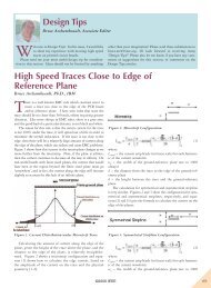
<strong>EMC</strong> DESIGN TIPS<br />
Bruce Archambeault<br />
IBM, P. O. Box 12195<br />
Department 18DA B306<br />
Research Triangle Park,<br />
NC 22709<br />
919.486.0120<br />
e-mail: bruce.arch@ieee.org<br />
COVER PHOTO/DESIGN ©<br />
Kenneth Wyatt<br />
www.wyattphoto.com<br />
Technical Editor<br />
Flavio Canavero<br />
Department of Electronics<br />
Polytechnic of Turin<br />
Corso Duca degli Abruzzi 24<br />
10129 Torino, Italy<br />
+39 (011) 564 4060<br />
fax: +39 (011) 564 4099<br />
e-mail: canavero@ieee.org<br />
<strong>EMC</strong> PERSONALITY PROFILE<br />
William G. Duff<br />
SENTEL, 7601 South Valley Drive<br />
Fairfax Station, VA 22039<br />
e-mail: wmduff@cox.net<br />
Frank Sabath<br />
WIS, Humboldstrasse<br />
D-29633 Munster, Germany<br />
+49.4172.988083<br />
Fax: +49.4172.988083<br />
e-mail: frank.sabath@ieee.org<br />
<strong>EMC</strong> STANDARDS ACTIVITIES<br />
Donald N. Heirman<br />
143 Jumping Brook Road<br />
Lincroft, NJ 07738-1442<br />
732.741.7723<br />
fax: 732.530.5695<br />
e-mail: d.heirman@worldnet.att.net<br />
<strong>EMC</strong>S BoD ACTIVITIES<br />
Janet Nichols O’Neil<br />
ETS-Lindgren<br />
1301 Arrow Point Drive<br />
Cedar Park, TX 78613<br />
425.868.2558<br />
fax: 425.868.0547<br />
e-mail: j.n.oneil@ieee.org<br />
<strong>EMC</strong>S EDUCATION<br />
COMMITTEE<br />
Tom Jerse, Professor<br />
The Citadel – Dept. of ECE<br />
171 Moultrie Street<br />
Charleston, SC 29409<br />
843.953.7499<br />
e-mail: Jerset@Citadel.edu<br />
<strong>EMC</strong> SOCIETY HISTORY &<br />
50th ANNIVERSARY<br />
Dan Hoolihan<br />
Hoolihan <strong>EMC</strong> Consulting<br />
P. O. Box 367<br />
Lindstrom, MN 55045<br />
651.213.0966<br />
fax: 651.213.0977<br />
e-mail: d.hoolihan@ieee.org<br />
Advertising Susan E. Schneiderman<br />
Business Development Manager, <strong>IEEE</strong> Magazines<br />
<strong>IEEE</strong> Media<br />
445 Hoes Lane,<br />
Piscataway NJ 08854 USA<br />
Tel: +1-732-562-3946; Fax: +1-732-981-1855<br />
www.ieee.org/ieeemedia ss.ieeemedia@ieee.org<br />
<strong>IEEE</strong> <strong>EMC</strong> <strong>Society</strong> Newsletter Publication Schedule<br />
Publication Editorial Advertising<br />
Dates Deadlines Deadlines<br />
Summer July 1 July 12<br />
Fall October 1 October 11<br />
Winter January 1 January 14<br />
Spring April 1 April 11<br />
<strong>IEEE</strong> <strong>EMC</strong> SOCIETY NEWSLETTER (ISSN 1089-0785) is published quarterly<br />
by the Electromagnetic Compatibility <strong>Society</strong> of the Institute of Electrical<br />
and Electronic Engineers, Inc., 3 Park Avenue, 17th Floor, New York, NY<br />
10016-5997. One dollar ($1.00 USD) per member per year (included in the<br />
<strong>Society</strong> fee) for each member of the <strong>EMC</strong> <strong>Society</strong>. Periodicals postage paid at<br />
New York, NY and additional mailing offices. This newsletter is printed in<br />
the USA. Postmaster: Send address changes to <strong>IEEE</strong> <strong>EMC</strong> <strong>Society</strong> Newsletter<br />
to 445 Hoes Lane, Piscataway, NJ 08854.<br />
© 2010 <strong>IEEE</strong>. Permission to copy without fee all or part of any material<br />
without a copyright notice is granted provided that the copies are not made<br />
or distributed for direct commercial advantage, and the title of the publication<br />
and its date appear on each copy. To copy material with a copyright<br />
notice requires specific permission. Please direct all inquiries or requests to<br />
<strong>IEEE</strong> Copyrights Office.<br />
ISSN 1089-0785<br />
<strong>IEEE</strong> prohibits discrimination, harassment, and bullying. For more information,<br />
visit http://www.ieee.org/web/aboutus/whatis/policies/p9-26.html.<br />
3
President’s Message<br />
Francesca Maradei, President, <strong>EMC</strong> <strong>Society</strong><br />
This message is written while I am right back from the most<br />
productive, exciting, and extremely tiring week of the year. I<br />
bet that all of you are able to guess that I am talking about the<br />
so-called “symposium week”. The 2010 <strong>IEEE</strong> International<br />
Symposium on <strong>EMC</strong> was held in Fort Lauderdale, Florida on<br />
July 25–30. I am sure that many of you are surprised to hear<br />
about the Symposium in the Summer issue. Traditionally, the<br />
Fall edition of the Newsletter is our “symposium issue”, where<br />
you can find pretty much everything you wanted to know<br />
about the annual Symposium. Well, consider this as a little<br />
anticipation. Much more will be reported in the following<br />
Newsletter edition.<br />
I want to take this opportunity to thank Fred Heather, 2010<br />
<strong>EMC</strong> Symposium General Chair, and his dedicated symposium<br />
committee for their efforts in making such a high-quality and<br />
extremely enjoyable event. Fort Lauderdale provided its “Caribbean<br />
style welcome” and an opportunity for us all to meet<br />
old friends and make new ones. The full week Symposium<br />
provided a wide offering which included workshops, tutorials,<br />
technical sessions, committee meetings, experiments,<br />
demonstrations, a technical exhibition, and the Global <strong>EMC</strong><br />
University program. Most will agree that the technical and social<br />
programs were outstanding, but honestly being in Florida<br />
wasn’t so shabby either!<br />
As usual, there is so much activity during the symposium<br />
week that it is often a challenge to keep track of the technical<br />
presentations, committee meetings, and social as well as<br />
private events that are scheduled. When I reflect on the week<br />
as a whole, a few memorable events stand out. Let me take a<br />
moment to highlight several of these standout moments from<br />
the Symposium.<br />
The Welcome Reception held at the Convention Center was<br />
for sure a memorable beginning. It started in the Exhibit Hall<br />
with a cocktail hour with our exhibitors and continued in the<br />
Grand Floridian Ballroom with a delicious Latin American buffet<br />
dinner. On one side of the big ballroom, an exclusive Latin<br />
Night Club with live music and professional salsa dancers provided<br />
a very enjoyable entertainment.<br />
The second very memorable social event was the Wednesday<br />
Gala Banquet. This year in Fort Lauderdale the banquet<br />
was held on the fabulous ocean view terrace of the Harbor<br />
Beach Marriott, and included, in addition to a great meal,<br />
also live dancing music in a perfect Floridian evening beach<br />
party style.<br />
The Awards Luncheon offered us another opportunity to recognize<br />
many of our <strong>Society</strong>’s leaders and technical contributors<br />
for 2009, as well as acknowledge several of our members who<br />
recently passed away. I had the pleasure of congratulating the<br />
winners and getting photos taken with them. The details of the<br />
awards and a listing of our worthy recipients will be included<br />
in the Fall Issue of the Newsletter.<br />
Finally, The Founder’s appreciation luncheon held during<br />
the week (arrangements courtesy of Dan Hoolihan) was very<br />
enjoyable. I had a chance to meet several Founders and past<br />
presidents. It was also a great opportunity to share past <strong>EMC</strong><br />
stories and other recollections. I am glad to see that this tradition<br />
that started on the occasion of the <strong>EMC</strong> <strong>Society</strong>’s 50th<br />
Anniversary is continuing.<br />
Letter from the Editor ....................3<br />
President’s Message ......................4<br />
Completed Careers ......................7<br />
<strong>EMC</strong> Personality Profile ..................8<br />
<strong>EMC</strong> <strong>Society</strong> History. ................... 10<br />
<strong>EMC</strong> <strong>Society</strong> Newsletter<br />
Review – 50-25-10 Years Ago ........... 10<br />
Obituaries in the <strong>EMC</strong> Newsletter ......... 13<br />
<strong>EMC</strong> Standards Activities from<br />
Summer 2000 Newsletter .............. 18<br />
<strong>EMC</strong>ABS. ............................20<br />
Practical Papers, Articles and Application Notes. ..26<br />
Gaps in the Application of the <strong>EMC</strong><br />
Directive Due to Inadequate Harmonized<br />
Product Standards ....................26<br />
EMI Failure Analysis Techniques:<br />
II. Joint Time-Frequency Analysis ........ 31<br />
Partial Inductance ......................34<br />
Creating Practical Experiments on <strong>EMC</strong> .....43<br />
<strong>EMC</strong> Standards Activity: We Need<br />
More “Smarts” for the <strong>EMC</strong> <strong>Society</strong><br />
Activity in Smart Grid................. 51<br />
Highlights of Connectivity Week 2010:<br />
<strong>EMC</strong> and Smart Grid.................. 51<br />
Book Reviews ..........................54<br />
Design Tips: Differential Signals are NOT<br />
Immune to EMI/<strong>EMC</strong> Concerns! ..........58<br />
Chapter Chatter.........................61<br />
Remembering Emeritus<br />
Professor Amemiya. . . . . . . . . . . . . . . . . . . . . 73<br />
The Importance of Technical<br />
Paper Writing ........................74<br />
Writing a Technical Paper.................74<br />
A Report on the 2010 Asia-Pacific<br />
International <strong>EMC</strong> Symposium in Beijing ...78<br />
Calendar ..............................85<br />
4
Photo by Ken Wyatt<br />
Milton Kant and Ralph Showers, Founders of the <strong>EMC</strong><br />
<strong>Society</strong>, while sitting in the <strong>EMC</strong> <strong>Society</strong> History Booth at<br />
the 2010 <strong>EMC</strong> Symposium in Fort Lauderdale.<br />
Speaking of Founders, I want to point out the very pleasant<br />
interview taken by Dan Hoolihan of the <strong>Society</strong> Founders: Milton<br />
Kant, Melvin First and Ralph Showers. The interview was<br />
recorded by Espresso Engineering and is posted on the <strong>EMC</strong><br />
<strong>Society</strong> website (www.emcs.org).<br />
Chapter Outreach Activity<br />
The annual Chapter Chair Training Session and dinner took place<br />
in Fort Lauderdale, Florida, in conjunction with the 2010 <strong>IEEE</strong><br />
<strong>EMC</strong> Symposium. Contrary to the past years schedule, in order to<br />
reduce the overlap with technical sessions and committee meetings,<br />
this year the training session was held on Monday afternoon<br />
followed by a dinner. Both events were well attended and provided<br />
the opportunity for exchanging valuable information between the<br />
chapter representatives and the <strong>EMC</strong> <strong>Society</strong>’s Global and Regional<br />
officers (e.g. VP for Member Services, Regional Membership and<br />
Chapter Coordinator, Regional Conference Coordinator). I would<br />
like to take this opportunity to recommend all the chapters plan to<br />
attend next year’s events during the 2011 <strong>EMC</strong> Symposium.<br />
As part of the global outreach activity, I was particularly glad<br />
to visit the <strong>IEEE</strong> <strong>EMC</strong> Seattle chapter which is one our most active<br />
chapters. The occasion that brought me to Seattle was the<br />
one day seminar entitled “The Latest Developments in Global<br />
<strong>EMC</strong> Commercial and Military Test Standards”, sponsored by<br />
the local chapter. The meeting was held on June 28, 2010 at<br />
The Museum of Flight. I had the privilege of being one of the<br />
speakers together with Don Heirman and Dave Walen. The<br />
event was very successful with 72 attendees and 24 exhibiting<br />
companies. I appreciated meeting the <strong>EMC</strong> <strong>Society</strong> members in<br />
the Seattle area, as well as having the opportunity to know more<br />
about the history of flight. I also particularly enjoyed sightseeing<br />
in the lovely city of Seattle and neighborhoods. I am<br />
very grateful to Janet O’Neil for her warm hospitality and for<br />
showing me the major city attractions in a very short time.<br />
Breaking News on <strong>EMC</strong> <strong>Society</strong> Publications<br />
The <strong>IEEE</strong> Transactions on <strong>EMC</strong> has increased its Impact Factor<br />
(IF) from 1.083 to 1.294. I am extremely proud of this<br />
outcome, especially because it was achieved without applying<br />
any artifact based on aggressive and unethical tactics as many<br />
other <strong>IEEE</strong> Societies do. The Electromagnetic Compatibility<br />
<strong>Society</strong> underwent a periodicals review on Thursday, 24 June<br />
2010 during the <strong>IEEE</strong> TAB meeting series in Montreal, Quebec,<br />
Canada. The review process with the Periodicals Review<br />
and Advisory Committee (PRAC) went well and the overall<br />
feedback received was very positive. A proposal to turn the<br />
Integrated<br />
ANTENNAS<br />
MICROWAVE CIRCUITS<br />
AND RADAR<br />
CROSS SECTION<br />
ANALYSIS<br />
SOFTWARE<br />
INTEGRATED’s tools provide solutions to<br />
a wide variety of electromagnetic field<br />
models, which can be obtained based on<br />
the Method of Moments (MoM) approach for<br />
open region problems and Finite Element<br />
Method (FEM) for closed region problems.<br />
Fast. Accurate. Easy-to-use.<br />
<br />
of complex geometric shapes<br />
<br />
Other benefits:<br />
<br />
<br />
Moment Method<br />
<br />
that handles Highly<br />
<br />
<br />
electrically large problems<br />
<br />
field distribution<br />
<br />
arbitrary, free form geometry<br />
<br />
software results with experimental results<br />
TRY OUR SOFTWARE FOR 30 DAYS!<br />
FREE EVALUATION<br />
<br />
LIVE DEMO<br />
+1.204.632.5636<br />
email info@integratedsoft.com or visit<br />
www.integratedsoft.com<br />
HYBRID SIMULATION TOOLS FOR<br />
ELECTROMAGNETIC DESIGN ANALYSIS<br />
integrated_newad_jk.indd 1<br />
5<br />
19/07/10 9:57 AM
Photos by Pat andre<br />
These photos are from the one day seminar at the Museum of Flight organized by the Seattle <strong>EMC</strong> Chapter.<br />
I am shown with two past presidents of the <strong>EMC</strong> <strong>Society</strong><br />
during my visit to Seattle: Don Heirman on the left and<br />
Len Carlson on the right.<br />
<strong>EMC</strong> Newsletter into a Magazine was also presented to the<br />
TAB Periodicals Committee on Thursday, 24 June 2010. <strong>IEEE</strong><br />
TAB approved unanimously the proposal allowing a successful<br />
completion of the phase 1 of the process. Phase 2 will occur<br />
next November and if successfully completed, the transition to<br />
an <strong>EMC</strong> Magazine will be effective starting January 2012.<br />
Board of Directors Meetings<br />
The second <strong>EMC</strong> <strong>Society</strong> Board of Directors (BoD) meeting in<br />
2010 was held in Fort Lauderdale on July 26 and 29, in conjunction<br />
with the annual <strong>EMC</strong> Symposium. A brief summary on the<br />
most important issues addressed during this meeting follows.<br />
• Four new Distinguished Lecturers were appointed for 2011–<br />
2012: Professor Chuck Bunting, Professor Wen-Yan Yin,<br />
Jerry Ramie, and Jerry Meyerhoff. These colleagues have a<br />
wide spectrum of expertise and experience, and all have industry<br />
experience as practicing engineers.<br />
• The venues for hosting the 2014–2016 <strong>EMC</strong> Symposia were<br />
selected:<br />
• The 2014 <strong>IEEE</strong> International Symposium on <strong>EMC</strong> will be<br />
held in Research Triangle Park, North Carolina<br />
• The 2015 <strong>IEEE</strong> International Symposium on <strong>EMC</strong> will be<br />
held in Dresden, Germany<br />
• The 2016 <strong>IEEE</strong> International Symposium on <strong>EMC</strong> will be<br />
held in Ottawa, Canada<br />
The next <strong>EMC</strong> <strong>Society</strong> Board of Directors (BoD) meeting<br />
is scheduled on November 13–14 in Pittsburgh and will host<br />
the Officer Elections. I remind everyone that all meetings<br />
of the <strong>EMC</strong> <strong>Society</strong> BoD are open. Any members who want<br />
to attend will be most welcome. The schedule of the BoD<br />
meeting is posted on the website at http://www.ewh.ieee.<br />
org/soc/emcs/conferences.html, and in the calendar section<br />
of the Newsletter.<br />
Call for Volunteers<br />
The success of our <strong>Society</strong> is possible thanks to many fine volunteers<br />
who have contributed unselfishly of their time and<br />
talent. As the <strong>Society</strong> evolves, and new initiatives emerge, we<br />
are always in need of volunteers. Please, give serious consideration<br />
to becoming involved in our broad and challenging goals<br />
and objectives. The full list of committees can be found on our<br />
website at http://www.ewh.ieee.org/soc/emcs/directors.html.<br />
I look forward to working with all of you who join the volunteers<br />
of the <strong>Society</strong> in helping achieve the set of our goals for<br />
the benefit of us all. For making a suggestion, comment, or just<br />
for dropping a friendly note, please do not hesitate to e-mail me<br />
at: fr.maradei@ieee.org.<br />
<strong>EMC</strong><br />
6
Completed Careers<br />
Don Heirman, Associate Editor<br />
Since the printing of the Spring 2010 issue of the <strong>EMC</strong><br />
Newsletter, it saddens me to report that Bill Rhoades<br />
passed away. Many thanks to Dan Hoolihan who provided<br />
the following tribute to Bill.<br />
I would like to continue to solicit your support in helping<br />
me receive the names of <strong>EMC</strong> <strong>Society</strong> members that have<br />
recently passed away. You can either forward them directly<br />
to your local Chapter chair, or if you don’t know who that<br />
is, you can forward the names to me (d.heirman@ieee.org)<br />
or a member of the Completed Careers Committee directly,<br />
including Bruce Archambeault, Don Sweeney, and Andy<br />
Drozd. See page 3 of this Newsletter or the <strong>EMC</strong> <strong>Society</strong><br />
website (www.emcs.org) for contact information of these<br />
committee members.<br />
Thank you in advance for your assistance as we honor<br />
<strong>EMC</strong> <strong>Society</strong> members who have completed their careers.<br />
Bill Rhoades, a long-time member of the<br />
<strong>EMC</strong> <strong>Society</strong> of the <strong>IEEE</strong>, passed away in<br />
March at the age of 79. Bill spent his entire<br />
career with Xerox and was a world-renowned<br />
specialist in Electromagnetic Compatibility<br />
Engineering.<br />
He followed the “technical ladder” at<br />
Xerox and was at the Principal Scientist<br />
level when he retired. He chaired an international<br />
standards committee internal to Xerox<br />
which was vital for the development of<br />
Xerox products.<br />
Joe Fischer, a Past-President of the <strong>EMC</strong><br />
<strong>Society</strong> and Technical Director for Fischer<br />
Custom Communications, worked with Bill<br />
at Xerox. He said, “As I remember Bill at<br />
Xerox, he was very analytical. When investigating any task, he<br />
would assure himself that no parameter was too small to have<br />
an effect on the outcome of a solution.”<br />
In the 1970s, Bill represented Xerox on Subcommittee 5 on<br />
Electromagnetic Interference which was part of the Environment<br />
and Safety Committee of the Computer and Business<br />
Equipment Manufacturers Association (CBEMA). Working<br />
cooperatively with representatives from Burroughs, Control<br />
Data, Digital Equipment, Eastman Kodak, Hewlett-Packard,<br />
Honeywell Information Systems, IBM, NCR, Sanders Data<br />
Systems, Sperry-Univac, and Tektronix; Bill and the Subcommittee<br />
developed a report called CBEMA/ESC5/77/29 in May<br />
of 1977. The title of the report was “Limits and Methods of<br />
William (Bill) Theodore<br />
Rhoades 1930–2010<br />
Measurement of Electromagnetic Emanations<br />
from Electronic Data Processing<br />
and Office Equipment.” This report was<br />
the basis for the United States Federal<br />
Communications Commission (FCC)<br />
Rules on Computers which were released<br />
in October of 1979 and which were part<br />
of FCC Docket 20780 proceedings.<br />
He published a number of papers on<br />
Lightning Effects, Electrostatic Discharge<br />
(ESD) and Power Line Disturbances.<br />
An example of one of his papers<br />
can be found in the 1988 <strong>IEEE</strong> International<br />
Symposium on <strong>EMC</strong> Proceedings,<br />
the paper is titled “Avoidance of<br />
ESD Effects” and it is located on Pages<br />
184–189 of that publication.<br />
At the time of his death, Bill was an active member of the<br />
United States Technical Advisory Group on CISPR I. (CISPR I<br />
is the Subcommittee that looks at “<strong>EMC</strong> of Information Technology,<br />
Multimedia Equipment, and Receivers;” it is part of CISPR<br />
which is the International Special Committee on Radio Frequency<br />
Interference.)<br />
Bill received his Bachelor of Science degree in Electrical<br />
Engineering from the Massachusetts Institute of Technology<br />
(MIT) in 1958. He also received his Master of Science degree in<br />
Electrical Engineering from MIT in 1959.<br />
Bill was living in Fullerton, California at the time of his<br />
death. He is survived by his wife, Patricia.<br />
<strong>EMC</strong><br />
7
<strong>EMC</strong> Personality Profile<br />
Dr. William G. Duff, Associate Editor<br />
The <strong>EMC</strong> personalities for this issue are our three new<br />
<strong>IEEE</strong> Fellows: Chris Holloway, Farhad Rachidi and<br />
Sabrina Sarto. Please join me in congratulating them for<br />
being elected to the Fellow Grade.<br />
Traditionally, I have included a profile for<br />
each of our new Fellows. However this year,<br />
one of our new Fellows, Farhad Rachidi, who<br />
was elected to the Fellow grade “for contributions<br />
to electromagnetic modeling”, was<br />
featured as the <strong>EMC</strong> personality profiled in<br />
the Spring issue of the <strong>EMC</strong> Newsletter. His<br />
profile will not be repeated in this issue.<br />
Our second new Fellow, Christopher<br />
L. Holloway, received the B.S.E. degree from<br />
the University of Tennessee at Chattanooga<br />
in 1986, and the M.S. and Ph.D. degrees<br />
from the University of Colorado at Boulder<br />
in 1988 and 1992, respectively, both in electrical<br />
engineering. Dr. Holloway was elected<br />
to the grade of Fellow “for the application of<br />
new materials in the field of electromagnetic compatibility.”<br />
Chris Holloway<br />
During 1992, he was a Research Scientist with Electro<br />
Magnetic Applications, Inc., in Lakewood, Colorado. His responsibilities<br />
included theoretical analysis and finite-difference<br />
time-domain modeling of various electromagnetic problems.<br />
From the fall of 1992 to 1994, he was with the National Center<br />
for Atmospheric Research (NCAR) in Boulder, Colorado.<br />
While at NCAR his duties included wave propagation modeling,<br />
signal processing studies, and radar systems design. From<br />
1994 to 2000, he was with the Institute for Telecommunication<br />
Sciences (ITS) at the U.S. Department of Commerce in Boulder,<br />
where he was involved in wave propagation studies. Since 2000,<br />
he has been with the National Institute of Standards and Technology<br />
(NIST) in Boulder, where he works on electromagnetic<br />
theory. He is also on the Graduate Faculty at the University of<br />
Colorado at Boulder.<br />
Dr. Holloway received the 2008 <strong>IEEE</strong> <strong>EMC</strong> <strong>Society</strong> Richard<br />
R. Stoddart Award, the 2006 Department of Commerce<br />
Bronze Medal for his work on radio wave propagation, the<br />
1999 Department of Commerce Silver Medal for his work in<br />
electromagnetic theory, and the 1998 Department of Commerce<br />
Bronze Medal for his work on printed circuit boards. He<br />
also has various best paper awards for both journal and conference<br />
publications.<br />
His research interests include electromagnetic field theory,<br />
wave propagation, guided wave structures, remote sensing, numerical<br />
methods, and <strong>EMC</strong>/EMI issues. Dr. Holloway is currently<br />
serving as co-chair for Commission A of the International<br />
Union of Radio Science and is an Associate Editor for the <strong>IEEE</strong><br />
Transactions on Electromagnetic Compatibility. Dr. Holloway was<br />
the chairman for the Technical Committee on Computational<br />
Electromagnetics (TC-9) of the <strong>IEEE</strong> Electromagnetic Compatibility<br />
<strong>Society</strong> from 2000–2005, served as an <strong>IEEE</strong> Distinguished<br />
Lecturer for the <strong>EMC</strong> <strong>Society</strong> from 2004–2006, and is<br />
currently serving as co-chair for the Technical Committee on<br />
Nano-Technology and Advanced Materials (TC-11) of the <strong>IEEE</strong><br />
<strong>EMC</strong> <strong>Society</strong>.<br />
Dr. Holloway holds U.S. Patents on<br />
electromagnetic absorbing materials, radar<br />
systems and antennas for atmospheric radars,<br />
and on volume measurements devices.<br />
He has over 190 technical publications; including<br />
journal articles, conference papers,<br />
book chapters, and technical reports.<br />
Dr. Holloway has two children. His<br />
son is a bassist in a heavy-metal band and<br />
has just released his first CD (www.myspace.com/centimani).<br />
His daughter is a<br />
sophomore at the University of Colorado<br />
studying environmental science. He loves<br />
the outdoors and when not playing with<br />
Maxwell’s equations, he can be found<br />
either riding his bicycle up-and-over some of the Colorado<br />
mountain passes, climbing rock faces, or in the winter, skiing<br />
the back country trails. His favorite saying is: “there is<br />
no such thing as bad weather, just bad clothing.” In the evenings,<br />
he is usually trying to figure-out how to play some<br />
convoluted guitar riff on his acoustic guitar. Finally, one of<br />
his more practical technical accomplishments is the design<br />
and development of the “Piaget Beer Gauge” (see www.<br />
thebeergauge.com). This is a measurement device designed<br />
to ensure one gets served a completely full pint (i.e., 16 oz) of<br />
beer at one’s favorite pub.<br />
Our third new Fellow, Maria Sabrina Sarto, was elected to the<br />
Fellow grade “for contributions to advanced materials in electromagnetic<br />
compatibility applications.”<br />
She received her Laurea, summa cum laude, and her Ph.D.<br />
degrees in Electrical Engineering from the University of Rome<br />
“La Sapienza” in 1992 and 1997, respectively.<br />
She was appointed Assistant Professor in 1994, Associate<br />
Professor in 1998 and Full Professor of Electrotechnics and<br />
Electromagnetic Compatibility at the Faculty of Engineering<br />
of Sapienza University of Rome in 2005.<br />
Dr. Sarto has served as Director of the Research Center on<br />
Nanotechnology Applied to Engineering of Sapienza, Director<br />
of the Electromagnetic Compatibility Laboratory of the<br />
Department of Electrical Engineering and the Scientific Coordinator<br />
of the Joint Lab on Micro/Nanotechnologies for industrial<br />
applications of Sapienza Innovation Consortium, and<br />
Director of the Nanotechnology and Nanoscience Laboratory<br />
of Sapienza.<br />
She has published more than 100 papers in the field of electromagnetic<br />
compatibility (<strong>EMC</strong>), numerical electromagnetics,<br />
and advanced materials for <strong>EMC</strong>. Current research interest<br />
8
includes carbon nanotube interconnects modeling and design,<br />
carbon nanotube and graphenebased<br />
nanomaterials for <strong>EMC</strong>, and <strong>EMC</strong><br />
in aerospace.<br />
Dr. Sarto has received numerous awards,<br />
including the Best Paper Award of the<br />
1993 <strong>IEEE</strong> International Symposium on<br />
<strong>EMC</strong> (Electromagnetic Compatibility) in<br />
Dallas; the Prize Paper Award of the <strong>IEEE</strong><br />
<strong>EMC</strong> <strong>Society</strong> for the best paper published<br />
in the international journal <strong>IEEE</strong> Transactions<br />
on <strong>EMC</strong> in 1997; the Prize Paper<br />
Award of the <strong>IEEE</strong> <strong>EMC</strong> <strong>Society</strong> for the<br />
best paper published in the international<br />
journal <strong>IEEE</strong> Transactions on <strong>EMC</strong> in 2000;<br />
the Best Paper Award of the International<br />
Symposium <strong>EMC</strong> Europe 2000 in Brugge;<br />
the Best Paper Award of the 2005 <strong>IEEE</strong><br />
Sabrina Sarto<br />
International Symposium on <strong>EMC</strong> in Chicago; the President’s<br />
Memorial Award of the <strong>IEEE</strong> <strong>EMC</strong> <strong>Society</strong> in 1996 and 1997;<br />
the Wright Brother Medal of the SAE (<strong>Society</strong> of Automotive<br />
Engineers) in 2002 and the “Sapienza<br />
Research Prize” in 2009 from Sapienza<br />
University of Rome.<br />
She was a Distinguished Lecturer of the<br />
<strong>IEEE</strong> <strong>EMC</strong> <strong>Society</strong> in 2001 and 2002. She<br />
has been an associate editor of <strong>IEEE</strong> Transactions<br />
on <strong>EMC</strong> since 1998, co-chair of the<br />
<strong>IEEE</strong> <strong>EMC</strong> <strong>Society</strong> TC-11 on “Nanotechnology<br />
and Advanced Materials”, member<br />
of the Advisory Board of the <strong>IEEE</strong> Council<br />
on Nanotechnology, and Chair of the<br />
Working Group for <strong>IEEE</strong> STD 299.1 of<br />
the <strong>IEEE</strong> <strong>EMC</strong> <strong>Society</strong>.<br />
In her spare time, Dr. Sarto enjoys playing<br />
tennis. During the winter, she loves<br />
downhill skiing and during the summer,<br />
sailing and wind surfing. She has been<br />
married to Fabio since 1999 and they have a beautiful 8-year<br />
old child, Alessio.<br />
<strong>EMC</strong><br />
Dedicated to Designing and Building<br />
State-of-the-Art Anechoic Chamber Facilities<br />
<br />
<br />
<br />
<br />
Over 50 years of construction experience<br />
Over 20 years of anechoic chamber design and manufacturing expertise<br />
Industry leader for custom-built, RF shielded facilities<br />
Dedication to quality, on-time delivery, and customer satisfaction<br />
Call Us Today at 717.263.4101<br />
Cuming Microwave Corporation<br />
T 508.580.2660 | 800.432.6464<br />
Avon, MA 02322 | CumingMW.com<br />
Cuming Lehman Chambers, Inc.<br />
T 717.263.4101<br />
Chambersburg, PA 17201 | CumingLehman.com<br />
DESIGN, ENGINEERING & CONSTRUCTION SERVICES | HOST STRUCTURES | ANECHOIC TEST CHAMBERS | MATERIALS DEVELOPMENT | RF & SPECIALTY ABSORBERS<br />
9
<strong>EMC</strong> <strong>Society</strong> History<br />
Daniel D. Hoolihan, Associate Editor, History Committee Chair<br />
Introduction to History Section<br />
For the Summer 2010 issue of the <strong>EMC</strong> Newsletter, we<br />
have three historically-oriented articles.<br />
The first is the standard “50–25–10 Years Ago” article<br />
which looks at Newsletter information from 50 years ago,<br />
25 years ago and 10 years ago.<br />
The second article reviews the obituaries that have been<br />
published in the <strong>EMC</strong> Newsletter. Over the years, a number<br />
of <strong>EMC</strong> <strong>Society</strong> Members have had their deaths noted in the<br />
pages of the Newsletter. A complete list, alphabetized by last<br />
name, is shown at the end of this article.<br />
The third article is titled, “History of Military <strong>EMC</strong><br />
Specifications.” This was written by long time members of<br />
the <strong>EMC</strong> <strong>Society</strong>, Herb Mertel and Warren Kesselman. It appeared<br />
in Issue No. 186, the Summer 2000 issue of the <strong>EMC</strong><br />
Newsletter as part of Don Heirman’s <strong>EMC</strong> Standards Activities<br />
column. With the surge of interest in the military <strong>EMC</strong><br />
standards these days, it seems appropriate to look back and<br />
see the commonalities of what we are still addressing today<br />
and yet see how far we’ve come with these specifications.<br />
Enjoy the history, both modern and ancient, of the <strong>EMC</strong><br />
<strong>Society</strong>!<br />
<strong>EMC</strong><br />
<strong>EMC</strong> <strong>Society</strong> Newsletter Review –<br />
50–25–10 Years Ago<br />
July – 1960 – Institute of Radio Engineers<br />
(IRE) Professional Group on Radio Frequency<br />
Interference (PGRFI) Newsletter – Number 12.<br />
The IRE PGRFI was the engineering<br />
organization that evolved into the present-day<br />
<strong>IEEE</strong> <strong>EMC</strong> <strong>Society</strong><br />
The Cover Stories of the July-1960 Newsletter included<br />
“Highlights of the Second National Symposium” and an article<br />
on the recently released Department of Defense Directive on a<br />
“Radio Frequency Compatibility Program.”<br />
The Second National Symposium on Radio Frequency Interference<br />
was held in Washington, DC on June 13 and 14, 1960.<br />
Total attendance was 406 people. The Best Technical Paper was<br />
given by Donald McClenon from the Naval Research Laboratory;<br />
its title was “Strong Signal Receiver Problems.” Extra<br />
copies of the Digest of the National Symposium were available<br />
through the PGRFI for a price of $2 per copy.<br />
MIL-STD 449 on “Measurement of Radio Frequency Spectrum<br />
Characteristics” was released for special distribution at the<br />
National Symposium.<br />
The Keynote speech of the Symposium was given by Henry<br />
Randall on the topic of “Getting on Top of the Nation’s RFI<br />
Prediction and Measurement Efforts.”<br />
The “Radio Frequency Compatibility Program” Directive<br />
established “A comprehensive program to cope with radio interference<br />
between electronic equipments and systems and, particularly,<br />
to ensure that, to the maximum practicable extent,<br />
electronic systems will not suffer operational degradation due<br />
to the absence of appropriate means for rejecting interference<br />
and for achieving radio frequency compatibility.”<br />
Specific objectives included:<br />
• Research and Development Area<br />
• Engineering Standards<br />
• Measurement Techniques and Test Procedures<br />
• Test Equipment<br />
• Equipment and System Characteristics<br />
• Tubes and Components<br />
• Education in Electronic Compatibility<br />
• Administration<br />
• Operational (Frequency Management) Area<br />
• Library of Spectrum Signatures<br />
• Environment File<br />
• Analysis Program<br />
• Allocation Procedures and Planning<br />
• Personnel<br />
• Administration<br />
Additional articles in the Newsletter included one on “AN/<br />
SPQ-5 RF Radiation Hazard Distance” and “Interference Makes<br />
News.”<br />
The Bureau of Ships Journal in June of 1960 made the<br />
following announcement: “Recent measurements of the AN/<br />
SPQ-5 radar have shown the maximum RF radiation hazard<br />
(RAD-HAZ) distance to the safe tolerance level (10 mW/<br />
cm 2 ) is 10 feet from the AN/SPQ-5 antenna. Where RAD-<br />
HAZ warnings have been posted on the basis of any previous<br />
distance, they are to be relocated in accordance with the new<br />
10-foot distance.”<br />
For the “Interference Makes News” article, Time magazine<br />
reported on June 4, 1960 the following news item: “Blue Network<br />
– In Lithgow, Australia, taxi drivers agreed to watch their<br />
10
Model FL7060<br />
2 MHz – 60 GHz range<br />
Model FL7040<br />
2 MHz – 40 GHz range<br />
Well actually, yes. These new laser-powered E-Field probes from AR are so versatile; they do the work of<br />
multiple probes, with outstanding accuracy and linearity for your demanding field monitoring requirements.<br />
They contain an internal microprocessor that provides advanced control and communication functions while<br />
automatically correcting for measurement drift caused by ambient temperature variations.<br />
Our newest laser probes are available in two models, which cover an exceptionally wide frequency range.<br />
Model FL7040 covers the 2 MHz – 40 GHz range while Model FL7060 covers the entire 2 MHz – 60 GHz range.<br />
So you don’t have to settle for what they have, but what you want. Being a laser probe you also have the<br />
convenience of never having to replace or recharge batteries. In addition, AR provides the largest family of probes<br />
in the industry.<br />
Like all AR products, our new probes are backed by the best and most comprehensive warranty<br />
along with the strongest support in the industry.<br />
To learn more, visit www. ar-worldwide.com or call us at 215-723-8181.<br />
NOTE: The FL7040 & FL7060 probes requires an FI7000 for power and communication.<br />
ISO 9001:2008<br />
Certified<br />
<br />
Other divisions: modular rf • receiver systems • ar europe<br />
USA 215-723-8181. For an applications engineer, call 800-933-8181.<br />
In Europe, call ar United Kingdom 441-908-282766 • ar France 33-1-47-91-75-30 • emv GmbH 89-614-1710 • ar Benelux 31-172-423-000<br />
Copyright © 2010 AR. The orange stripe on AR products is Reg. U.S. Pat. & TM. Off.
language after some of their two-way radio communications<br />
were accidentally broadcast over the loudspeaker in Our Lady<br />
of Fatima Church.”<br />
Rexford Daniels was the editor of the Newsletter.<br />
Twenty-Five Years Ago –<br />
Issue No. 126 – Summer-1985<br />
The Cover Story of this Newsletter was the “1985 <strong>IEEE</strong> International<br />
Symposium on <strong>EMC</strong>.” The symposium was to be held<br />
August 20–22, 1985 at the Colonial Hilton in Wakefield, Massachusetts.<br />
The theme of the Symposium was “<strong>EMC</strong> – A Universal<br />
Goal.” Dr. Chester L. “Chet” Smith was the Symposium<br />
Chairman.<br />
Eugene Knowles was President of the <strong>EMC</strong> <strong>Society</strong>, the<br />
Secretary was Don Clark, and the Treasurer was Len Carlson.<br />
Bob Haislmaier was Technical Director for Communications<br />
Services, Ed Bronaugh was Technical Director for Technical<br />
Services, Fred Nichols was Technical Director for Member<br />
Services, and Dr. Sato was Technical Director for Professional<br />
Services.<br />
Terry Cantine was the <strong>EMC</strong> Personality Profile. Chapter<br />
Chatter included reports from Atlanta, Central New England,<br />
Chicago, Littleton (Colorado), Los Angeles, New Jersey Coast,<br />
San Diego, Santa Clara Valley, Seattle, Tokyo, and a new Chapter<br />
from the Twin Cities of Minnesota!<br />
Gilda Haskins was selected as “1984 Young <strong>EMC</strong> Engineer<br />
of the Year.” She was a member of the Board of Directors of the<br />
<strong>EMC</strong> <strong>Society</strong>.<br />
Institutional Listings on the back cover of the Newsletter<br />
included: Electro-Metrics (a Division of Penril Corp);<br />
Tecknit EMI Shielding Products; Radiation Sciences, Inc.;<br />
Spectrum Control, Inc.; LectroMagnetics, Inc.; Amador Corporation;<br />
Genisco Technology Corporation; Chomerics, Inc.;<br />
Schaffner <strong>EMC</strong>, Inc.; Don White Consultants, Inc.; Universal<br />
Shielding Corporation; Honeywell, Inc.; and G&H Technology,<br />
Inc.<br />
Robert D. Goldblum was the Editor of the Newsletter;<br />
Associate Editors included Charles F.W. Anderson (Chapter<br />
Chatter), James S. Hill (Book Reviews), William G. Duff (Personality<br />
Profiles), Dr. G. Robert Redinbo (Sequency Union),<br />
Melvin J. Johnson (Abstracts), Fred J. Nichols (Photographer),<br />
Richard B. Schulz (<strong>EMC</strong> Standards Activities), Henry Ott<br />
(<strong>EMC</strong> <strong>Society</strong> Education Committee), Donald N. Heirman<br />
(<strong>EMC</strong> <strong>Society</strong> BOD Activities), Anthony G. Zimbalatti (Point<br />
and Counterpoint), Edwin Bronaugh (Short Papers, Articles,<br />
and Application Notes), and Walt McKerchar (Inter-<strong>Society</strong><br />
Activities).<br />
Ten Years Ago – Issue No. 186 –<br />
Summer-2000<br />
The cover story of this issue of the <strong>EMC</strong> Newsletter was an<br />
obituary for Motohisa Kanda who was born on September 10,<br />
1943 and passed away on June 12, 2000. Moto was most wellknown<br />
to <strong>EMC</strong> members in his role as Editor-in-Chief of the<br />
<strong>IEEE</strong> Transactions on <strong>EMC</strong> for 12 years. He was also an <strong>IEEE</strong> Fellow.<br />
He was the group leader for the Fields and Interference<br />
Group of NIST in Boulder, Colorado for fifteen years. He was also<br />
an adjunct Professor in the Department of Computer Engineering<br />
at the University of Colorado. He received many <strong>IEEE</strong> Awards<br />
(including the <strong>EMC</strong> <strong>Society</strong>’s Laurence G. Cumming Award for<br />
Outstanding Service to the <strong>Society</strong> in 1999) and other United<br />
States Department of Commerce awards during his career. The<br />
Newsletter included a one-page tribute from Atsuya Maeda to his<br />
friend and professional colleague, Dr. Moto Kanda.<br />
The Newsletter also contained an article on “<strong>EMC</strong> Chapter<br />
Funds Scholarship Endowment for San Francisco State University.”<br />
This was a story written by Franz Gisin, a Santa Clara<br />
Valley Chapter Member, on how the Santa Clara Valley Chapter<br />
donated $16,000 to the San Francisco State University to “Promote<br />
<strong>EMC</strong> Education.” The interest from the Endowment will<br />
be used to sponsor scholarships for outstanding electrical engineering<br />
students who are focusing their area of specialization<br />
in the fields of <strong>EMC</strong> and EMI. The story included a picture of<br />
Dr. Zorica Pantic-Tanner, chair of the Santa Clara Valley <strong>EMC</strong><br />
Chapter, delivering a check to Joy Morimoto, Senior Development<br />
Officer, Office of University Development, at San Francisco<br />
State University.<br />
Bob Rothenberg, the Associate Editor of “Practical Papers,<br />
Articles, and Application Notes”, had two short articles in<br />
his area of the Newsletter. The first was “On No! Where’s the<br />
Grounding Post? – An Early Japanese Polar <strong>EMC</strong> Story” by<br />
Takeo Yoshino. This article talked about Dr. Yoshino’s experiences<br />
with grounding electronic systems and power systems<br />
in the harsh environment of Antarctica. The story of how he<br />
developed a unique “counter-poise” grounding system to solve<br />
interference issues is very informative. The second article was<br />
a story by Douglas C. Smith on “A Resistive Current Probe.”<br />
The story highlights a simple, but effective, troubleshooting<br />
tool for analyzing emissions and ESD events at the circuit<br />
board level.<br />
The Personality Profile in this issue is Elya Bernard Joffe.<br />
The <strong>EMC</strong> Standards Activities article, as edited by Donald<br />
Heirman was titled “The History of Military <strong>EMC</strong> Specifications”<br />
by Warren Kesselman and Herbert Mertel. The article<br />
has been reprinted in this issue of the Newsletter.<br />
The Editor of the Newsletter was Janet O’Neil. <strong>EMC</strong><br />
12
Obituaries in the <strong>EMC</strong><br />
Newsletter<br />
Introduction<br />
Over the years, a number of <strong>EMC</strong> <strong>Society</strong> Members have had<br />
their deaths noted in the pages of the <strong>IEEE</strong> <strong>EMC</strong> <strong>Society</strong> Newsletter.<br />
The total number of notifications is around 67 people.<br />
The complete list, alphabetized by last name, is shown at the<br />
end of this article. Of course, many well-respected individuals<br />
who were members of the <strong>EMC</strong> <strong>Society</strong> were not honored in the<br />
Newsletter due to a lack of feedback from family members who<br />
did not know we offer that compliment to the members at the<br />
end of their career.<br />
Cover Page Remembrances<br />
Although most of our members are memorialized within the<br />
pages of the body of the Newsletter, some key contributors to<br />
the <strong>Society</strong> are honored with a cover page memorial. There have<br />
been a total of 10 individuals honored in this fashion.<br />
The first was Maximilian Ware who was honored in Newsletter<br />
#37 in March of 1965. He was chairman of the Washington<br />
Chapter of the <strong>EMC</strong> <strong>Society</strong>. He was a pioneer in the<br />
Government radio frequency compatibility efforts in the Office<br />
of the Chief Signal Officer and initiated the first government<br />
contracts for Radio Frequency Interference (RFI) studies and<br />
measurements by the Armour Research Foundation and the<br />
Georgia Institute of Technology.<br />
Aaron Humphrey Sullivan, Jr. was the second individual<br />
honored on the cover page of the Newsletter; Issue No.<br />
124 in the Winter of 1985. He was knows as “Sully” to his<br />
friends and he was a Founding Member of the Washington<br />
Chapter of the <strong>EMC</strong> <strong>Society</strong>. He served on the Board of Directors<br />
of the <strong>EMC</strong> <strong>Society</strong> from 1964 to 1969 and from<br />
1973 to 1975. He was Chairman of the 1983 Silver Anniversary<br />
Symposium held in Washington, DC. He believed that<br />
every man owes something to the advancement of his profession<br />
and “Sully” achieved this in his service to the <strong>IEEE</strong> and<br />
the <strong>EMC</strong> <strong>Society</strong>.<br />
The third individual was Rexford Daniels who was a Founding<br />
Member of the Institute of Radio Engineers (IRE) Professional<br />
Group on RFI; the predecessor to the <strong>IEEE</strong> <strong>EMC</strong> <strong>Society</strong>.<br />
“Rex” was born on June 16, 1898 and passed away on January<br />
2, 1987. He was the first Newsletter Editor of the <strong>EMC</strong><br />
<strong>Society</strong>; he actually started a newsletter called “Quasies and<br />
Peaks” in 1954 before the start of the <strong>EMC</strong> <strong>Society</strong> in 1957<br />
and that became the basis for the newsletter of the IRE Professional<br />
Group on RFI. He served as Editor of the newsletter<br />
from 1957 until the middle of 1968. He was also President of<br />
the <strong>EMC</strong> <strong>Society</strong> from 1965–1967. “Rex” was the first recipient<br />
of the <strong>EMC</strong> <strong>Society</strong> Certificate of Appreciation, the <strong>EMC</strong><br />
<strong>Society</strong> Certificate of Recognition, and the <strong>EMC</strong> <strong>Society</strong> Honorary<br />
Life Membership.<br />
Harold Raymond Schwenk was a Founding Member and the<br />
first Chairman of the IRE Professional Group on RFI and served<br />
from 1957 until 1959 in that role. He was born on November<br />
1, 1923 and died on March 27, 1988. He was also a Founder<br />
of the Metropolitan New York <strong>EMC</strong> <strong>Society</strong> Chapter and was<br />
Chairman of that Chapter a number of times.<br />
James Stewart Hill was the fifth individual honored on the<br />
cover page of the <strong>EMC</strong> Newsletter. He was a Founding Member<br />
of the IRE Professional Group on RFI and was an Associate Editor<br />
of the <strong>EMC</strong> Newsletter for Book Reviews for over twenty<br />
years. He was born on December 2, 1912 and his last day with<br />
us was October 30, 1988.<br />
Fred J. Nichols was the next individual to be honored on the<br />
cover page. He was a Founder of the IRE Professional Group on<br />
RFI and President of the <strong>EMC</strong> <strong>Society</strong> in 1969. He was wellknown<br />
for his photographs at <strong>EMC</strong> Symposiums and for founding<br />
LectroMagnetics, Inc. (a shield room company). He was<br />
also the father of our present Newsletter Editor, Janet Nichols<br />
O’Neil. Fred lived from 1917 to 1990.<br />
Gerald Rothhammer was another Founder of the IRE<br />
Professional Group on RFI and a popular member of the<br />
<strong>EMC</strong> <strong>Society</strong>. He was involved with companies that developed<br />
EMI instrumentation for almost forty years. He was a<br />
Member of the Board of Directors of the <strong>EMC</strong> <strong>Society</strong> and<br />
he served as Assistant Director of Professional Services on<br />
the Board for a number of years. His time on earth was from<br />
1930 to 1991.<br />
The early 1990s were a sad time for the <strong>EMC</strong> <strong>Society</strong>. The<br />
next outstanding individual to die in the early “90s” and to be<br />
honored on the cover page of the Newsletter was Dr. Robert<br />
J. Haislmaier. He served on the <strong>EMC</strong> <strong>Society</strong> Board of Directors<br />
for a number of years and was Director of Communication<br />
Services on the Board. He was elected a Fellow of the <strong>IEEE</strong> in<br />
1987. He lived from June 26, 1929 until January 11, 1992.<br />
The ninth member of the <strong>EMC</strong> <strong>Society</strong> to be honored on the<br />
cover page of the Newsletter was Richard B. Schulz who lived<br />
from May 21, 1920 to October 1, 1998. He was honored on<br />
Issue No. 180 for the Winter of 1999. Richard was primarily<br />
known for serving as Editor of the <strong>IEEE</strong> Transactions on Electromagnetic<br />
Compatibility for 18 years. He had numerous other<br />
achievements in his career including serving as President of the<br />
<strong>EMC</strong> <strong>Society</strong> Board of Directors in 1968. He was also a Life<br />
Fellow of the <strong>IEEE</strong>.<br />
The tenth member of the <strong>EMC</strong> <strong>Society</strong> to be listed in memoriam<br />
on the cover page of the Newsletter was Motohisa Kanda.<br />
He was honored in Issue #186 in the Summer of 2000. He was<br />
most well-known for being Editor of the <strong>IEEE</strong> Transactions on<br />
<strong>EMC</strong> for 12 years. He was an <strong>IEEE</strong> Fellow. He was with us from<br />
September 10, 1943 until June 12, 2000.<br />
Other Facts<br />
It is interesting to note that two of our most “remembered”<br />
members both passed away in the 1972–1973 timeframe<br />
and were highlighted in the Newsletter; Richard R. Stoddart<br />
and Laurence Gordon Cumming. Two of the most significant<br />
awards in the <strong>EMC</strong> <strong>Society</strong> are named in honor of<br />
these two gentlemen.<br />
13
The only woman on the list was L. Gilda Haskins-McMahon<br />
who was honored in Newsletter #170 which was released in the<br />
Summer of 1996. Her life duration was 1949–1996.<br />
Since 2000, we have honored 34 individuals in the <strong>EMC</strong> <strong>Society</strong><br />
for their lives of service to the <strong>IEEE</strong> and the <strong>EMC</strong> <strong>Society</strong>.<br />
This is approximately as many as we had honored in the first 43<br />
years of our existence as an Engineering <strong>Society</strong>.<br />
In the Spring Issue of 2008, an <strong>EMC</strong> <strong>Society</strong> “Completed<br />
Careers” Committee was formed “with the goal of making sure<br />
<strong>EMC</strong> <strong>Society</strong> Members who pass away are recognized and honored.”<br />
Part of the Committee’s responsibility is to publish information<br />
on members who have “completed their careers” in<br />
the <strong>EMC</strong> Newsletter. The Completed Careers column is now a<br />
regular part of the <strong>EMC</strong> Newsletter.<br />
Obituaries in the eMC sOCiety newsletter<br />
Compiled by Daniel D. Hoolihan – Chair – History Committee <strong>EMC</strong> <strong>Society</strong>—<strong>IEEE</strong><br />
# Newsletter Number Date Name Life Duration Front Cover<br />
th25 162 SUM-1994 Akao, Yasuo 1922–1994<br />
13 123 FAL-1984 Bailey, Stuart Lawrence 1905–1984<br />
49 213 SPR-2007 Brook, Robert H.<br />
36 192 WIN-2002 Bush, Donald R. 1942–2001<br />
65 224 WIN-2010 Calcavecchio, Ralph J. 1929–2009<br />
41 201 SPR-2004 Crawford, Myron Lloyd 1938–2004<br />
7 79 FAL-1973 Cumming, Laurence Gordon 1902–1973<br />
17 133 SPR-1987 Daniels, Rexford 1898–1987 YES<br />
28 172 WIN-1997 Davis, Michael 1960–1996<br />
5 66 OCT-1970 Dietrich, Terry W.<br />
9 85 SPR-1975 Dinger, Harold Eugene<br />
37 192 WIN-2002 Doeppner, Thomas W. 1920–2001<br />
18 134 SUM-1987 Eckersley, Alfred E.<br />
45 210 SUM-2006 Fisher, Joseph James (Navy Joe) 1923–2006<br />
29 175 FAL-1997 Garlan, Herman 1908–1997<br />
12 119 FAL-1983 Green, William C. 1910–1983<br />
3 50 OCT-1967 Gregory, Charles A.<br />
34 188 WIN-2001 Gross, Al 1918–2000<br />
53 215 FAL-2007 Haber, Fred 1921–2007<br />
24 152 WIN-1992 Haislmaier, Robert J. 1929–1992 YES<br />
52 215 FAL-2007 Hall, Ken 1943–2007<br />
51 214 SUM-2007 Hart, Michael J. 1952–2007<br />
26 170 SUM-1996 Haskins-McMahon, L. Gilda 1949–1996<br />
21 140 WIN-1989 Hill, James Stewart 1912–1988 YES<br />
44 210 SUM-2006 Hish, Delbert Mark (Andy) 1923–2006<br />
19 134 SUM-1987 Johnson, Melvin J. 1940–1987<br />
11 108 WIN-1981 Johnson, William R. 1931–1980<br />
33 186 SUM-2000 Kanda, Motohisa 1943–2000 YES<br />
14
42 201 SPR-2004 Kendall, Chris 1941–2004<br />
56 218 SUM-2008 Knoller, Hank 1933–2008<br />
30 176 WIN-1998 Knowles, Eugene Daniel 1921–1997<br />
38 192 WIN-2002 Krevsky, Seymour 1921–2001<br />
58 219 FAL-2008 McKerchar, Walter D. 1929–2008<br />
59 220 WIN-2009 Middleton, David 1920–2008<br />
61 221 SPR-2009 Nalbandian, Sr., Andrew John 1929–2009<br />
22 148 WIN-1991 Nichols, Fred 1917–1990 YES<br />
50 214 SUM-2007 O’Neil, John J. 1914–2007<br />
57 219 FAL-2008 Ooi, Ban-Leong 1967–2008<br />
55 217 SPR-2008 Osburn, John Duncan McMillan 1940–2008<br />
15 129 SPR-1986 Pakala, William Elmer 1901–1985<br />
35 189 SPR-2001 Parker, Al 1914–2001<br />
27 170 SUM-1996 Parker, James C.<br />
62 221 SPR-2009 Parker, William (Bill) Harvey 1946–2009<br />
43 210 SUM-2006 Perini, Jose 1928–2006<br />
1 14 NOV-1960 Potter, E. Vernon<br />
4 62 DEC-1969 Pratt, Haradan 1891–1969<br />
48 213 SPR-2007 Renner, John Joseph 1920–2007<br />
67 226 SUM-2010 Rhoades, William T. 1930–2010<br />
66 225 SPR-2010 Robertson, Douglas W. 1924–2010<br />
23 150 SUM-1991 Rothhammer, Gerald P. 1930–1991 YES<br />
39 195 FAL-2002 Rowe, Aubrey James 1942–2002<br />
8 79 FAL-1973 Schultz, Harold R.<br />
31 180 WIN-1999 Schulz, Richard B. 1920–1998 YES<br />
20 138 SUM-1988 Schwenk, Harold Raymond 1923–1988 YES<br />
10 99 FAL-1978 Siegfried, Victor<br />
46 211 FAL-2006 Smith, Jr., Albert Aloysius<br />
6 76 JAN-1973 Stoddart, Richard R. 1900–1972<br />
14 124 WIN-1985 Sullivan, Jr., Aaron Humphrey 1915–1985 YES<br />
16 130 SUM-1986 Taylor, Ralph Edward 1923–1985<br />
47 213 SPR-2007 Thomas, Sr., Leonard William 1910–2007<br />
40 199 FAL-2003 Tokumaru, Shinobu 1941–2003<br />
63 221 SPR-2009 Toller, Lawrence (Larry) Joseph 1927–2009<br />
64 222 SUM-2009 Trefney, Ralph 1940–2009<br />
60 221 SPR-2009 Vance, Edward F. 1929–2008<br />
54 216 WIN-2008 Violette, Joseph L. N. (Norm) 1932–2008<br />
2 37 MAR-1965 Ware, Maximilian 1901–1964 YES<br />
32 180 WIN-1999 Zajac, Herb<br />
<strong>EMC</strong><br />
15
The Technical Program for the 2011 <strong>IEEE</strong> International<br />
Symposium on <strong>EMC</strong> in Long Beach, California will have<br />
something for everyone — from the novice <strong>EMC</strong> engineer<br />
to the advanced practitioner. The technical papers have<br />
enjoyed a reputation for extremely high quality in the past<br />
years, and <strong>EMC</strong> 2011 will be no different!<br />
In fact, I am excited and pleased to announce that<br />
the <strong>EMC</strong> 2011 Symposium will have guest speakers who<br />
are the top leaders in their respective fields. This is a unique<br />
opportunity to see these technical giants in person!<br />
<br />
The Long Beach Convention & Entertainment<br />
Center is a spectacular multi-purpose complex<br />
- one of the few waterfront facilities nationwide -<br />
featuring more than 400,000 square feet of flexible<br />
exhibit and meeting space, two theaters, an arena<br />
and 34 meeting rooms. The glass concourse and<br />
lobby offer expansive views of the scenic harbor and<br />
downtown skyline.<br />
Located in the heart of downtown Long Beach,<br />
the Center is within walking distance to first-class<br />
accommodations, shopping, dining, attractions,<br />
sightseeing along picturesque bays and 5 1/2 miles<br />
of sandy beach.<br />
• Henry Ott will teach the fundamentals of <strong>EMC</strong> based on<br />
his award-winning book, Electromagnetic<br />
Compatibility Engineering<br />
• Dr. Howard Johnson will organize a special session on<br />
Signal Integrity<br />
Technical papers will cover a wide range of topics including<br />
<strong>EMC</strong> Measurements, EMI Control, Computational<br />
Electromagnetics, Signal Integrity, High Power<br />
Electromagnetics, <strong>EMC</strong> Management, Electromagnetic<br />
Environments, as well as the newest technical topic areas<br />
for the <strong>EMC</strong> <strong>Society</strong>: Nanotechnology, Engineered<br />
Materials, and Smart Grid.<br />
Remember, for the latest research in <strong>EMC</strong> – visit us in<br />
Long Beach!
210<br />
1<br />
<br />
<strong>EMC</strong> 2011 is a Technical<br />
Symposium. Technical Papers<br />
are the essence of our Technical<br />
Program. Original, unpublished<br />
papers on all aspects of<br />
electromagnetic compatibility<br />
are invited.<br />
*Late papers will NOT be accepted<br />
10<br />
110<br />
405
<strong>EMC</strong>ABS<br />
<strong>EMC</strong> Abstracts<br />
Osamu Fujiwara, Associate Editor<br />
<strong>EMC</strong>ABS Committee<br />
Bob Hunter, Consultant<br />
r.d.hunter@ieee.org<br />
Sha Fei, <strong>EMC</strong> Research Section, Northern Jiatong<br />
University, Beijing, China<br />
emclab@center.njtu.edu.cn<br />
Ferdy Mayer, 7, rue Paul Barruel, F-75015 Paris, France<br />
ferdymayer@free.fr<br />
Maria Sabrina Sarto, Department of Electrical Engineering,<br />
University of Rome, Italy<br />
sarto@elettrica.ing.uniroma1.it<br />
“How Can I Get a Copy<br />
of an Abstracted Article?”<br />
Engineering college/university libraries, public libraries, company<br />
or corporate libraries, National Technical Information<br />
Services (NTIS), or the Defense Technical Information Center<br />
(DTIC) are all possible sources for copies of abstracted articles<br />
or papers. If the library you visit does not own the source<br />
document, the librarian can probably request the material or a<br />
copy from another library through interlibrary loan, or for a<br />
small fee, you can order it from NTIS or DTIC. Recently it<br />
became clear that <strong>EMC</strong>ABs were more timely than publications<br />
which were being listed in data files. Therefore, additional<br />
information will be included, when available, to assist<br />
in obtaining desired articles or papers. Examples are: <strong>IEEE</strong>,<br />
SAE, ISBN, and Library of Congress identification numbers.<br />
As the <strong>EMC</strong> <strong>Society</strong> becomes more international, we will be<br />
adding additional worldwide abstractors who will be reviewing<br />
articles and papers in many languages. We will continue<br />
to set up these informal cooperation networks to assist members<br />
in getting the information or contacting the author(s).<br />
We are particularly interested in symposium proceedings<br />
which have not been available for review in the past. Thank<br />
you for any assistance you can give to expand the <strong>EMC</strong>S<br />
knowledge base.<br />
<strong>EMC</strong><br />
<strong>EMC</strong>ABS: 01-08-2010<br />
INFLUENCE OF DEVICE STRUCTURE ON ELECTROMAG-<br />
NETIC (EM) INFORMATION LEAKAGE FROM THE DEVICE<br />
+ Kouhei Ohmura, ++ Yu-ichi Hayashi, +++ Takaaki Mizuki<br />
and +++ Hideaki Sone<br />
+ Graduate School of Information Science, Tohoku University,<br />
6–3 Aramaki Aza Aoba, Aoba-ku, Sendai, 980–8578 Japan<br />
++ Graduate School of Engineering, Tohoku University, 6–3<br />
Aramaki Aza Aoba, Aoba-ku, Sendai, 980–8578 Japan<br />
+++ Cyberscience Center, Tohoku University, 6–3 Aramaki Aza<br />
Aoba, Aoba-ku, Sendai, 980–8578 Japan<br />
a9im4007@s.tohoku.ac.jp<br />
Proc. of 4th Pan-Pacific <strong>EMC</strong> Joint Meeting, May 27–28, 2010/<br />
Sendai, Japan, pp. 19–22.<br />
Abstract: A working information device radiates electromagnetic<br />
(EM) field around itself, and the problem is known that<br />
the information leaks via the EM field. The device which consists<br />
of a printed circuit board (PCB) and attached lines<br />
behaves as a frequency filter, through which the EM field is<br />
emanated. In this paper, the authors show the filter frequency<br />
characteristics depend on the number of attached lines, on the<br />
length of the attached line and on the size of the PCB. These<br />
results imply that we should pay more attention to the device<br />
structure, and that we can suppress the EM information leakage<br />
by considering the structure.<br />
Index terms: Electromagnetic information leakage, printed circuit<br />
board, frequency filter, device structure.<br />
<strong>EMC</strong>ABS: 02-08-2010<br />
A MEASUREMENT METHOD FOR 2-D EMF DISTRIBU-<br />
TIONS USING OPTICAL TRACKER<br />
+ Ken Sato, + Toshiaki Kawata and + Yoshitsugu Kamimura<br />
+ Graduate School of Engineering, Utsunomiya University 7-1-2<br />
Yoto, Utsunomiya-shi, Tochigi, 321-8585 Japan<br />
satok@m.ieice.org<br />
Proc. of 4th Pan-Pacific <strong>EMC</strong> Joint Meeting, May 27–28, 2010/<br />
Sendai, Japan, pp. 27–29.<br />
Abstract: Recently, we have proposed the freehand scanning<br />
method for measuring field distribution using a magnetic<br />
tracker to determine the position of an EMF sensor. However,<br />
a magnetic tracker cannot obtain correct location data if there<br />
are some metals around the measurement area though it has<br />
enough accuracy for determining the position. In this study,<br />
an optical tracker that consists of the USB camera and PC with<br />
Open CV is used instead of a magnetic tracker to determine<br />
the measurement position. As a result, it is found that an optical<br />
tracker is useful for the real-time, rough measurement of<br />
2-D field distribution.<br />
Index terms: Measurement method for 2-D field distribution,<br />
optical tracker, EMF sensor, real-time freehand scan.<br />
20
<strong>EMC</strong>ABS: 03-08-2010<br />
CONSERVATIVE CALCULATION OF WHOLE-BODY<br />
AVERAGED SARS OVER 1 GHZ IN INFANTS<br />
+ Hironobu Miwa, + Akimasa Hirata, + Osamu Fujiwara, ++<br />
Tomoaki Nagaoka and ++ Soichi Watanabe<br />
+ Department of Computer Science and Engineering, Nagoya<br />
Institute of Technology, Gokiso-cho, Showa-ku, Nagoya 466-<br />
8555 Japan<br />
++ National Institute of Information and Communications<br />
Technology 4-2-1 Nukuikitamachi, Koganei, Tokyo, 160-8582,<br />
Japan<br />
fujiwara@odin.nitech.ac.jp<br />
nagaoka@nict.go.jp<br />
wata@nict.go.jp<br />
Proc. of 4th Pan-Pacific <strong>EMC</strong> Joint Meeting, May 27–28, 2010/<br />
Sendai, Japan, pp. 43–46.<br />
Abstract: We previously showed that conservative estimates of<br />
whole-body-average specific absorption rates (WBA-SARs) in<br />
children can be given by homogeneous ellipsoids having the<br />
same physique, and also that our proposed formula for calculating<br />
GHz-band WBA-SARs in terms of height and weight provides<br />
conservative WBA-SARs in infants with the median<br />
height and the Kaup index of 0.5 percentile. In this study, we<br />
compared WBA-SARs at frequencies over 1 GHz in infants<br />
calculated from their corresponding homogeneous ellipsoids<br />
with conservative estimates from the formula to reveal that the<br />
<strong>EMC</strong>C<br />
DR. RAŠEK<br />
EMP<br />
TM<br />
GENERATORS<br />
• LEMP-DO 160: SW, LW, DSW per RTCA-DO-160<br />
• LEMP-EFA 1: per EFA/SPE-J-E-1000 up to 80MW<br />
• LEMP-EFA 2: per EFA, SPE-J-000-E-1000<br />
• NEMP-EFA 1: DSW 2-50-100MHz, 10kV!<br />
• NEMP-EFA 2: 5ns/24ns, up to 50kV/m<br />
• EMP-461 C6 DSW: per MIL 461, 10kHz to 100MHz<br />
• LEMP-IEC-DSW: per IEC 61000-4-12, 100kHz/1MHz<br />
• MBG-1M/10M/800V: Multiburst AIRBUS, BOEING, SAE<br />
• LEMP-MIL 1757, "Big Bang". STANAG, DEF-STAN<br />
ALL TESTS IMMEDIATELY AT THE<br />
<strong>EMC</strong>C TEST LABS OR ON-SITE<br />
<strong>EMC</strong>Comp DR. RAŠEK<br />
Moggast, Boelwiese 6 • 91320 Ebermannstadt<br />
Germany<br />
T: + 49 - 91 94 - 90 16 • F: + 49 - 91 94 - 81 25<br />
emc.comp@emcc.de • www.emcc.de<br />
<strong>EMC</strong>, RADIO, TELECOM<br />
ENVIRONMENT, SAFETY<br />
formula gives approximately the same and conservative estimates<br />
as those from the ellipsoids with 2/3-muscle and muscle<br />
tissues, respectively.<br />
Index terms: Infants, whole-body averaged SARs, Kaup index,<br />
conservative calculation.<br />
<strong>EMC</strong>ABS: 04-08-2010<br />
PHYSICS-BASED MODELING OF DGS FILTER FORMED<br />
ON RETURN PLANE OF PRINTED CIRCUIT BOARDS<br />
+ Keisuke Matsumoto, + Yoshitaka Toyota y, + Kengo Iokibe<br />
and + Ryuji Koga<br />
+ Graduate School of Natural Science and Technology, Okayama<br />
University 3-1-1, Tsushima-Naka Kita-ku Okayama-shi,<br />
700-8530 JAPAN<br />
Fmatsumoto@dev.cne.okayama-u.ac.jp<br />
Toyota@dev.cne.okayama-u.ac.jp<br />
Iokibe@dev.cne.okayama-u.ac.jp<br />
koga@dev.cne.okayama-u.ac.jp<br />
Proc. of 4th Pan-Pacific <strong>EMC</strong> Joint Meeting, May 27–28, 2010/<br />
Sendai, Japan, pp. 51–54.<br />
Abstract: The slit pattern formed on the return plane of printed<br />
circuit boards (PCBs) acts like a passive element and a<br />
defected ground structure (DGS) is one of them. The characteristics<br />
of DGS are easily varied with the slit pattern. Thus,<br />
DGS is expected to be used for various applications. Since a<br />
design method has yet to be developed, however, we need to<br />
establish a design method for the slit pattern. Some equivalent<br />
circuit models have been used, but the models that consist<br />
of lumped elements require a full-wave simulation. In<br />
addition, the values of the lumped elements do not relate to<br />
the physical parameters. Therefore, it is not useful for<br />
designing filters. In contrast, the equivalent circuit model we<br />
propose in this paper will have a great contribution to designing<br />
filters with optimum performances because the transmission<br />
line model relates to the physical parameters. As a result,<br />
by comparing the transmission characteristics calculated with<br />
both a full-wave and a circuit simulator with the proposed<br />
equivalent circuit model, the first stop-band width was in<br />
agreement.<br />
Index terms: Printed circuit boards, slit pattern, return plane,<br />
defected ground structure filter.<br />
<strong>EMC</strong>ABS: 05-08-2010<br />
A BRIEF MODEL OF THE COMMON-MODE EXCITA-<br />
TION IN NON-UNIFORM TRANSMISSION LINES<br />
+ Ryuji Koga<br />
+ Professor Emeritus, Okayama University 6-20-3, Tsushima-<br />
Fukui-1, Kita-ku, Okayama 700-0080, Japan<br />
koga@cne.okayama-u.ac.jp<br />
Proc. of 4th Pan-Pacific <strong>EMC</strong> Joint Meeting, May 27–28, 2010/<br />
Sendai, Japan, pp. 71–74.<br />
Abstract: The common mode is excited when two transmission<br />
lines with different cross-sectional profiles are connected even<br />
if perfect differential mode current is injected into one of the<br />
lines. A simple model to evaluate the quantity of the common<br />
mode current/voltage is proposed and exemplified of its convenience.<br />
The issue is made under the proposition that the com-<br />
22
mon mode is very weak in comparison to that of differential<br />
mode in an actual electric device which is conscious of EMI:<br />
TEM mode is almost retained over the two lines.<br />
Index terms: Non-uniform transmission lines, EMI, commonmode<br />
excitation model.<br />
<strong>EMC</strong>ABS: 06-08-2010<br />
TECHNICAL TRENDS IN HIGH-SPEED POWER LINE<br />
COMMUNICATION<br />
+ Masamitsu Tokuda<br />
+ Department of Information Network Engineering, Tokyo<br />
City University 1-28-1 Tamazutsumi, Setagaya-Ku, Tokyo,<br />
158–8557 Japan<br />
mtokuda@tcu.ac.jp<br />
Proc. of 4th Pan-Pacific <strong>EMC</strong> Joint Meeting, May 27–28, 2010/<br />
Sendai, Japan, pp. 103–106.<br />
Abstract: High-speed power line communication (PLC) can<br />
transmit an information signal of several hundred megabits per<br />
second over the power lines that transport electrical energy.<br />
Because this system employs unmodified existing transmission<br />
lines and the signal can be accessed through the simple interface<br />
of an ordinary electrical outlet, it promises to serve as the<br />
most effective transmission system for supporting information<br />
in home appliances. For high-speed PLC to become practical, it<br />
requires that the frequencies used be expanded to 30 MHz, a<br />
frequency band that is already used by many wireless communication<br />
systems. Thus, shared use with<br />
those systems is the most important problem.<br />
This paper introduces technical trends<br />
related to that issue.<br />
Index terms: Power line communication,<br />
electrical outlet, information home appliances,<br />
transmission system.<br />
between the power line and residence has been given. Finally, it<br />
gives the ordinary permissible exposure limits in China.<br />
Index terms: Low frequency electromagnetic bioeffect, 3-phase<br />
symmetrical power transmission line, AC electrified railways,<br />
minimum permissible separation distance, ordinary permissible<br />
exposure limits.<br />
<strong>EMC</strong>ABS: 08-08-2010<br />
REVIEW OF THE DEVELOPMENT OF BREAST CANCER<br />
DETECTION SYSTEM USING MICROWAVE TOMOGRA-<br />
PHY TECHNOLOGY<br />
+ Jeong-Ki Pack, + Tae-Hong Kim and ++ Soon-Ik Jeon<br />
+ Radio Department, Chungnam National University, 220<br />
Gung-dong Yuseong-gu, Daejeon, 305–764, South KOREA<br />
++ Antenna Research Team, ETRI, 161 Gajeong-dong Yuseonggu,<br />
Daejeon, 305–700, South KOREA<br />
jkpack@cnu.ac.kr<br />
thkim@cnu.ac.kr<br />
sijeon@etri.re.kr<br />
Proc. of 4th Pan-Pacific <strong>EMC</strong> Joint Meeting, May 27–28, 2010/<br />
Sendai, Japan, pp. 163–166.<br />
Abstract: In this paper, the breast cancer detection system under<br />
development is reviewed. The system consists of RF sensing, signal<br />
processing, digital signal processing, system control and monitoring<br />
parts. This is the microwave tomography system operating in the<br />
frequency range of 500–3000 MHz. To solve the inverse scattering<br />
<strong>EMC</strong>ABS: 07-08-2010<br />
SOME RESEARCH WORKS ON LOW<br />
FREQUENCY ELECTROMAGNETIC<br />
BIOEFFECT IN CHINA<br />
+ Gao Yougang, Li Li, + Shi Dan and +<br />
Jiang Xiao<br />
+ P.O.Box 171, Beijing University of Posts<br />
and Telecom, Beijing, 100876, China<br />
Proc. of 4th Pan-Pacific <strong>EMC</strong> Joint Meeting,<br />
May 27–28, 2010/Sendai, Japan, pp.<br />
139–151.<br />
Abstract: People pay much attention to low<br />
frequency electromagnetic bioeffects these<br />
days. This work gives the general formula for<br />
calculating the electric fields around a<br />
3-phase symmetrical power transmission line<br />
when the heights of its conductors are different<br />
from each other. It gives also the method<br />
for calculating electric fields around asymmetrical<br />
lines and the method for calculating<br />
magnetic field around power transmission<br />
lines and AC electrified railways. The minimum<br />
permissible separation distance<br />
23
problem, we used the FDTD (Finite Difference Time Domain) for<br />
the forward problem and the Gauss-Newton method as the optimization<br />
algorithm. The results of the reconstructed image showed<br />
that we can detect the position of the tumor exactly.<br />
Index terms: Breast cancer detection system, microwave tomography<br />
technology, inverse scattering problem, FDTD simulation.<br />
<strong>EMC</strong>ABS: 09-08-2010<br />
BROADBAND COMMON-MODE NOISE REJECTION FOR<br />
GHZ DIFFERENTIAL SIGNALS USING DEFECTED<br />
GROUND STRUCTURES<br />
+ Chung-Hao Tsai and + Tzong-Lin Wu<br />
+ Graduate Institute of Communication Engineering, National<br />
Taiwan University Taipei, 10617 Taiwan<br />
wtl@cc.ee.ntu.edu.tw<br />
Proc. of 4th Pan-Pacific <strong>EMC</strong> Joint Meeting, May 27–28, 2010/<br />
Sendai, Japan, pp. 189–190.<br />
Abstract: A wideband and compact filter design for commonmode<br />
noise suppression in high-speed differential signals is<br />
proposed. It is based on two U-shaped and one H-shaped coupled<br />
patterned ground structures. An equivalent lumped model<br />
of three coupled LC resonators to predict the common-mode<br />
suppression characteristics is also developed. The model shows<br />
a good agreement to the full-wave simulation and measurement<br />
result. A test sample is designed and fabricated on a standard<br />
PCB. It is found the common-mode noise can be reduced by the<br />
filter over 15 dB from 3.6 GHz to 9.1 GHz.<br />
Index terms: GHz differential signals, common-mode noise rejection,<br />
defected ground structures, wideband and compact filter<br />
design.<br />
<strong>EMC</strong>ABS: 10-08-2010<br />
HOW TO ENHANCE <strong>EMC</strong> SELF-LEARNING<br />
+ Werachet Khan-Ngern<br />
+ Faculty for Engineering, King Mongkut’s Institute of Technology<br />
Ladkrabang (KMITL), Bangkok 10520, Thailand<br />
kkveerac@kmitl.ac.th<br />
kkveerac@yahoo.com<br />
Proc. of 4th Pan-Pacific <strong>EMC</strong> Joint Meeting, May 27–28, 2010/<br />
Sendai, Japan, pp. 219–222.<br />
Abstract: The paper presents the aspect of enhancing <strong>EMC</strong> self-learning<br />
using the simplicity of tools and equipment, IT media and demonstration.<br />
The proposed model of <strong>EMC</strong> self-learning is presented.<br />
The <strong>EMC</strong> concept is introduced. Then, some <strong>EMC</strong> self-learning<br />
examples are presented. The <strong>EMC</strong> study base on radiated EMI<br />
emission is demonstrated by the comparison between the <strong>EMC</strong><br />
testing with and without <strong>EMC</strong> design.<br />
Index terms: <strong>EMC</strong> self-learning, EMI emission, <strong>EMC</strong> testing,<br />
<strong>EMC</strong> design, demonstration.<br />
<strong>EMC</strong>ABS: 11-08-2010<br />
DEVELOPMENT OF LOW-FREQUENCY, WIDEBAND<br />
MAGNETIC FIELD DOSIMETER AND ITS APPLICATION<br />
TO MEASUREMENT OF CONDUCTED EMISSION FROM<br />
APPLIANCES<br />
+ Kenichi Yamazaki and + Kiyotomi Miyajima<br />
+ Central Research Institute of Electric Power Industry, 2-6-1<br />
Nagasaka, Yokosuka-shi, Kanagawa, 240-0196 Japan<br />
yamazaki@criepi.denken.or.jp<br />
Proc. of 4th Pan-Pacific <strong>EMC</strong> Joint Meeting, May 27–28, 2010/<br />
Sendai, Japan, pp. 239–242.<br />
Abstract: A low-frequency, wideband (25 Hz–100 kHz) magnetic<br />
field dosimeter was developed and applied to characterize<br />
conducted emissions (noise current) generated by consumer<br />
appliances such as IH (induction heating) cookers and PVC<br />
(photo voltaic conditioner). The result showed that the magnetic<br />
field sensors were successfully applicable to characterize<br />
the conducted emissions without splitting conductors of<br />
cables.<br />
Index terms: Consumer appliances, conducted emissions, lowfrequency<br />
wideband magnetic field dosimeter, development.<br />
<strong>EMC</strong>ABS: 12-08-2010<br />
A UNIFIED PHANTOM FOR THE SAR COMPLIANCE<br />
TEST OF MOBILE PHONES<br />
+ Lira Hamada,++ Takahiro Iyama, + Teruo Onishi and ++<br />
Soichi Watanabe<br />
+ National Institute of Information and Communications Technology,<br />
4-2-1, Nukuikitamachi, Koganei, Tokyo 184–8795,<br />
Japan<br />
++ NTT DOCOMO, INC., 3–6, Hikarino-oka, Yokosuka,<br />
Kanagawa 239-8536, Japan<br />
hamada@nict.go.jp<br />
Proc. of 4th Pan-Pacific <strong>EMC</strong> Joint Meeting, May 27–28, 2010/<br />
Sendai, Japan, pp. 243–246.<br />
Abstract: For the compliance test of mobile phones, the Specific<br />
Anthropomorphic Mannequin (SAM) phantom is used as the<br />
standardized human head. This measurement procedure is<br />
highly reliable; however, a simplified test procedure is needed<br />
for the reduction of the measurement number per one phone.<br />
Therefore, a simplified phantom (Uniphantom) has been proposed,<br />
which is a unification of the SAM and the flat phantom<br />
for body-worn device measurement. As a preliminary study,<br />
applicability of this phantom to the compliance test of various<br />
mobile phones is presented.<br />
Index terms: Compliance test, specific anthropomorphic mannequin<br />
(SAM) phantom, simplified uniphantom, body-worn<br />
device measurement.<br />
<strong>EMC</strong><br />
24
Practical Papers, Articles<br />
and Application Notes<br />
Flavio Canavero, Technical Editor<br />
In this issue, you will enjoy reading three very interesting<br />
and varied contributions.<br />
The first article is entitled “Gaps in the Application of<br />
the <strong>EMC</strong> Directive Due to Inadequate Harmonized Product<br />
Standards” by Frank Leferink, <strong>EMC</strong> Authority at Thales and<br />
Professor with Twente University, in the Netherlands. This<br />
contribution illustrates, with the support of in-situ measurements,<br />
the change of scenario that man-made electromagnetic<br />
noise underwent in the last decades with respect to the traditional<br />
noise signatures, mainly determined in the first half of<br />
the 20th century, that represent the basis for the standards. The<br />
explosion of the number of sources in the domestic, industrial,<br />
commercial, etc. environments, and the change of signal transmission<br />
type (from analogue to digital) require a reconsideration<br />
of the standards, since the producers of electronic goods<br />
must assure the proper functioning of their products in the real<br />
environment, and not only the compliance to <strong>EMC</strong> directives.<br />
I’m sure that the paper will stimulate the discussion on the<br />
intrinsic requirements for compliance.<br />
The second article is entitled “EMI Failure Analysis Techniques:<br />
Part II on Joint Time-Frequency Analysis” by Weifeng<br />
Pan and David Pommerenke from the <strong>EMC</strong> Lab of Missouri<br />
University of Science and Technology in Rolla, Missouri. This is<br />
the second contribution of a series covering different methods for<br />
EMI failure analysis of devices. This paper focuses on the time evolution<br />
of measured spectra that may reveal interesting features<br />
not detectable by separate time or frequency domain analyses.<br />
The last article traditionally presents a contribution belonging<br />
to the “Education Corner” series. This time I offer you a<br />
well-thought article on “Partial Inductance” authored by Professor<br />
Clayton R. Paul. This article complements a sequence<br />
of two papers on inductance calculation (by the same author)<br />
that appeared in 2008. Several misconceptions and confusion<br />
exists on inductance, and Professor Paul, with his pedagogical<br />
style, unveils the mysteries and takes us to a complete understanding<br />
of the subtleties of this critical parameter.<br />
In conclusion, I encourage (as always) all readers to actively<br />
participate to this column, either by submitting manuscripts<br />
they deem appropriate, or by nominating other authors having<br />
something exciting to share with the Community. I will<br />
follow all suggestions, and with the help of independent reviewers,<br />
I really hope to be able to provide a great variety of<br />
enjoyable and instructive papers. Please communicate with<br />
me, preferably by email at canavero@ieee.org.<br />
Gaps in the Application of the <strong>EMC</strong><br />
Directive Due to Inadequate Harmonized<br />
Product Standards<br />
Frank Leferink, Technical Authority <strong>EMC</strong> THALES Netherlands;<br />
Full-professor <strong>EMC</strong>, University of Twente, The Netherlands;<br />
Frank.Leferink@UTwente.nl - frank.leferink@nl.thalesgroup.com<br />
Abstract—For planning wireless communication systems the<br />
noise levels outside buildings have been used. The ITU<br />
(International Telecommunication Union) man-made noise<br />
levels are based on measurements performed in the 1970s.<br />
Measurements carried out since then showed that the noise<br />
caused by ignition systems reduced, but man-made noise in<br />
business areas and city centers increased. But the interference<br />
scenario changed: from analog communication systems in<br />
relatively free space to digital systems in living areas, often<br />
semi-enclosed such as offices, industrial production areas,<br />
and even cars and trains. Measurements in these semi-enclosed<br />
environments show a much higher, up to 60dB, manmade<br />
noise level. The higher noise level is not only due to a<br />
shorter distance to the source of emission, but mainly due to<br />
mistakenly assumption that compliance with a harmonized<br />
product standard is sufficient evidence of compliance with<br />
the European <strong>EMC</strong> directive. This is an incorrect and a<br />
wrong assumption. The <strong>EMC</strong> directive gives essential requirements<br />
to comply with. The use of harmonized product standards<br />
only gives a presumption of conformity. In a court case<br />
in a dispute on <strong>EMC</strong> of an electrical wheelchair, the key reference<br />
was the essential requirements and not the harmonized<br />
product standards. Several product standards have been<br />
developed with relaxed, or sometimes even no requirements.<br />
Some allow unlimited emission levels while others restricted<br />
the frequency range. These standards, although harmonized,<br />
are not in line with the essential protection requirements of<br />
the <strong>EMC</strong> directive.<br />
26 ©2010 <strong>IEEE</strong>
Man-Made Noise<br />
The knowledge of the electromagnetic ambient, or radio, noise<br />
is of particular interest in planning and setting up wireless systems,<br />
and as such to estimate the risk and impact of electromagnetic<br />
interference (EMI). Radio noise external to the radio<br />
receiving system derives from either natural, such as atmospheric<br />
and galactic noise and lightning, or unintended radiation from<br />
electrical and electronic equipment, power transmission lines,<br />
including railway systems, and internal combustion engines.<br />
This unintended radiation is called man-made noise (MMN) and<br />
is assumed to comprise two dominant and distinct components:<br />
white Gaussian noise (WGN) and impulsive noise (IN).<br />
The levels for radio, including man-made, noise are usually<br />
taken from the ITU-R 372-8 [1]. The levels in that document<br />
are based on measurements made in the 60s and 70s in the<br />
United States [2].<br />
The noise power in an equivalent lossless antenna can be<br />
replaced by the man-made noise, where the measured field<br />
strength, using an isotropic antenna with gain 1 and no losses,<br />
in a measuring bandwidth b is converted to the noise figure F a .<br />
In logarithmic units this becomes<br />
F aM 5 E n 1 95 2 20 log f MHz 2 10 log b [dB] (1)<br />
Probabilistic descriptions of the received noise waveform are<br />
required to determine system performance and the amplitude<br />
probability distribution (APD) (exceedance probability) of the<br />
received envelope is used. The most important minimum expected<br />
median values of F a is shown in Figure 1, taken from [1].<br />
Technology changed considerably in the last decades, as well<br />
as the use of wireless systems. Some measurement campaigns have<br />
been carried out to update the man-made noise levels [3, 4, 5, 6,<br />
7, 8, 9, 10, 11]. In [3] measurements performed in business areas<br />
of Montreal and Ottawa, and in residential Ottawa are described<br />
showing that there has been no significant increase of the MMN,<br />
but even a decrease in noise level, caused in part by the practice of<br />
using buried power lines rather than overhead power lines.<br />
In 1970s, a significant component of man-made noise in VHF<br />
(30–300MHz) is due to ignition impulses from motor vehicles.<br />
Measurements show now that this automobile noise is no longer<br />
a significant VHF noise source, but that now computers were<br />
found to be capable of generating a significant amount of noise<br />
[6]. A follow-up report on Man-Made Noise power measurements<br />
at VHF and UHF frequencies [7] concluded that 402.5<br />
MHz UHF noise levels in business areas were high enough to<br />
adversely affect communication system performance some of<br />
the time. The communication office in the United Kingdom<br />
awarded a contract in 2001 for setting up a measurement facility<br />
for measuring the man-made noise in various areas and<br />
measurement results have been published in 2003 [8]. MMN<br />
data has been collected in 8 locations: (large) city centre, factory<br />
estate, business centre, town centre, shopping centre/mall,<br />
major highway, suburban, and rural, at mid-morning, evening,<br />
and the rush hour. The study concludes that the decreasing level<br />
with frequency is as in the ITU report [1], but that the overall<br />
level is substantially higher. The highest MMN levels were<br />
found at the city centre, the factory estate and at the business<br />
centre. The road junction showed lower results, which again<br />
shows the effectiveness of measures taken via European legislation<br />
to reduce the automobile ignition noise. Measurements in<br />
Sweden [9] show lower noise levels than the ITU levels, except<br />
Noise Figure Above kTB (dB)<br />
120<br />
110<br />
100<br />
90<br />
80<br />
70<br />
60<br />
50<br />
40<br />
30<br />
20<br />
10<br />
0<br />
–10<br />
0.1 1 10 100 1,000<br />
Frequency (MHz)<br />
.<br />
ITU-R P.372-8 Atmospheric Noise<br />
ITU-R P.372-8 Galactic Noise<br />
ITU-R P.372-8 Business<br />
ITU-R P.372-8 Business Area Man-Made Noise<br />
ITU-R P.372-8 Residential<br />
ITU-R P.372-8 Rural<br />
ITU-R P.372-8 Quiet Rural<br />
ITU-R P.372-8 Man-Made Noise, Quiet Receiving Site<br />
Fig. 1. Minimum expected median values of F a .<br />
Noise Figure Above kTB (dB)<br />
120<br />
110<br />
100<br />
90<br />
80<br />
70<br />
60<br />
50<br />
40<br />
30<br />
20<br />
10<br />
0<br />
0.1 1 10 100 1,000<br />
Frequency (MHz)<br />
ITU-R P.372-8 Business Area Man-Made Noise<br />
ITU-R P.372-8 Business<br />
ITU-R P.372-8 Residential<br />
OFCOM AY4119 Business Centre<br />
OFCOM AY4119 City Centre<br />
OFCOM AY4119 Factory Estate<br />
Almere, Production Plant<br />
Belgium 3, During Lunch Time<br />
Belgium 1 Belgium 2 Belgium 3<br />
Iwama Hengelo<br />
Fig. 2. Noise levels outside buildings and in semi-enclosed,<br />
industrial, environments. The lines within the ellipsoid are<br />
the noise levels outside buildings.<br />
for urban areas and the city of Stockholm where the MMN was<br />
up to 15dB higher. Iwama [10] showed a much higher MMN<br />
at the lower frequencies, in the HF region, decreasing faster in<br />
UHF region.<br />
Figure 2 gives the values for F a for man-made noise as collected<br />
in the last decade.<br />
It is remarkable that nearly to no data is available on the EM ambient<br />
in living, often semi-enclosed, environments. Semi-enclosed<br />
©2010 <strong>IEEE</strong><br />
27
Fig. 3. Some of the semi-enclosed, industrial, environments where EM ambient surveys have been performed.<br />
environments are sites such as production plants, offices, houses<br />
and even include cars, trains or planes. Wireless communication<br />
systems are being used more and more in these semi-enclosed<br />
environments, while the interference model is based on the conventional<br />
assumption that free-space radio communication systems<br />
has to be protected. An additional issue is the multiple reflections<br />
inside semi-enclosed environments at VHF and UHF, where the<br />
wavelength of the noise is smaller than the dimension of the semienclosed<br />
environment. These multiple reflections are scattering<br />
MMN and radio waves erratically, and interfering with or blocking<br />
wireless transmissions [12]. EN 61000-2-5 [13] provides some<br />
guidance for the characterization of the electromagnetic ambient<br />
levels under different circumstances. However, the electromagnetic<br />
environment inside transportation equipment, vehicles, traction,<br />
ships & aircraft, is not described. A guide to establish the EM ambient<br />
is given in [14]. NIST (National Institute Science Technology,<br />
Boulder, USA) performed tests (no reference, data taken from press<br />
news) in manufacturing plants crowded with stationary and mobile<br />
metal structures, such as fabrication and testing machinery, platforms,<br />
fences, beams, conveyors, mobile forklifts, maintenance vehicles<br />
and automobiles in various stages of production. The survey<br />
showed that interference from heavy equipment can impair wireless<br />
communication signals such as those used in some controllers<br />
on the production floor.<br />
Within the frame of COST 286, several institutes performed<br />
site surveys in industrial environments [11], including KHBO<br />
Brugge-Oostende, University of Liege (both Belgium), University<br />
of Catalunya (Spain), University of Hannover (Germany),<br />
University of Twente (Netherlands). Measurements have been<br />
performed in HF, VHF and UHF bands. Based on these surveys<br />
noise figure curves have been added, as shown in Figure 2. Pictures<br />
of some of the environments are shown in Figure 3.<br />
The difference in man-made noise level looks enormous,<br />
and it is. The large increase is due to the high emission level<br />
of machinery controlled by computers, frequency converters<br />
and valves. These machines have to fulfill rather relaxed and<br />
high radiated emission levels at a distance of 10 m to 30 m.<br />
In the survey we investigated the emission levels around these<br />
machines with measuring distances sometimes less than 2 m.<br />
One measurement was performed during lunch time. Comparing<br />
the results on average the MMN decreased by 40dB during<br />
this break, proving that the electrical and electronic equipment<br />
was the source.<br />
Interference Case<br />
In the 1970s the then man-made noise is mainly due to ignition<br />
impulses from motor vehicles. This has changed to MMN due<br />
to the use of electrical equipment [6], sometimes high enough<br />
to adversely affect communication system performance [7].<br />
Most existing radio receivers are designed for the case of<br />
additive white Gaussian noise (WGN), and their performance<br />
may deteriorate in other scenarios, for example when subjected<br />
to impulsive noise [9]. In rural environments the man-made<br />
noise can be approximated as WGN, but in urban and sub-urban<br />
environments the man-made noise is often impulsive noise<br />
(IN). For digital communication systems, WGN does not represent<br />
a major problem as long as the mean power of the desired<br />
received signal is high enough.<br />
The IN is harmful for digital communication because each<br />
pulse may cause bursts of bit errors and loss of synchronization.<br />
An extreme example of underestimating the MMN is the German<br />
Toll project [15, 16]. Several billions of euros were lost<br />
due to interference in GPS receivers in industrial areas and city<br />
centers, and the system had to be redesigned causing a long<br />
delay without income (of toll).<br />
Another key issue is the classic interference case. This assumes<br />
a source of noise, on the road or from a neighbor, which<br />
is interacting with the wanted signal received with an antenna<br />
placed on the rooftop of a building, as shown in Figure 4 and 5.<br />
In our modern living environment many electronic systems<br />
are used, including wireless communication systems. Especially<br />
in the transport sector a huge increase of wireless control systems<br />
can be observed, from the wireless bridge control systems on large<br />
cruise-liners, to the next generation passenger planes. This interference<br />
case, where many systems are packed in semi-enclosed<br />
environments, is not taken into account by most standards. In<br />
industrial production plants many wireless systems are already<br />
in use and many interference problems had to be solved, such as<br />
disturbed wireless data transmission in the 433 MHz band.<br />
European Emission Standards<br />
In the last decade a plethora of new product standards have<br />
been published, especially (driven) by European companies.<br />
Due to a lack of a generic standard, based on a proper description<br />
of the electromagnetic environment in which the product<br />
would be used, two product standards have been selected as<br />
28 ©2010 <strong>IEEE</strong>
‘generic’ standard: the EN55022 for household and office environments,<br />
and the EN55011 for the industrial environment.<br />
Parallel to these generic standards, product standards have been<br />
developed. As an example, the EN55015 is the product family<br />
standard for electrical lighting and similar equipment. The<br />
frequency range covered is 9 kHz to 400 GHz, but the 1996<br />
version contains no requirements for radiated emissions from<br />
30 MHz and above. The Swedish Authority has found that<br />
some halogen lighting sets which are powered by an electronic<br />
transformer cause radiated emissions in frequencies not covered<br />
by EN 55015 [19]. When they tested it against the generic<br />
standards they found that the apparatus exceeded the limit by<br />
30 dB and 31 dB at 30.72 MHz, and the disturbance level was<br />
extensive up to 50 MHz. The EN 55015 has been upgraded<br />
and now contains requirements up to 300 MHz [20].<br />
The manufacturers of frequency converters had problems<br />
to fulfill the generic standards and used the same trick: they<br />
developed the IEC 61800-3 and EN 61800-3 on <strong>EMC</strong> for Adjustable<br />
Speed Electrical Power Drive Systems (PDS) [21]. Instead<br />
of leaving out a frequency range, complete categories were<br />
excluded. In the standard it is written ‘Where a PDS does not<br />
comply with the limits of category C1, the following warning shall<br />
be included in the instructions for use: Warning: In a domestic environment,<br />
this product may cause radio interference, in which case<br />
supplementary mitigation measures may be required ’. Does such a<br />
product not produce interference in other environments than<br />
the domestic environment? For equipment of category C2 an<br />
‘information requirement’ has been added: ‘If a PDS does not meet<br />
the limits of category C1 or C2, a warning shall be included in the<br />
instructions for use stating that: this type of PDS is not intended to be<br />
used on a low-voltage public network which supplied domestic premises;<br />
radio frequency interference is expected if used on such a network. The<br />
manufacturer shall provide a guide for installation and use, including<br />
recommended mitigation devices’. We asked a manufacturer for the<br />
recommended mitigation devices. The answer was that such a<br />
filter did not exist…. In one case we asked for measurement<br />
results of a PDS, in this case conducted emission. After several<br />
months and many repeated requests we received the data, showing<br />
compliance with the standard, and an overall emission level<br />
of 45 dBmV. But the equipment caused interference problems<br />
so we performed measurements. The emission level was 130<br />
dBmV, 75 dB above the limit of the generic standard, and 85<br />
dB above the level stated by the manufacturer. When confronted<br />
with this huge difference the manufacturer did not respond<br />
for 6 months, and finally replied with the statement that the<br />
wrong data had been sent erroneously…. The PDS appeared to<br />
be a C2 type, which actually means that the emission level is<br />
unlimited. Because the EN 61800-3 is a harmonized standard,<br />
a presumption of conformity with the <strong>EMC</strong> Directive [17] exists,<br />
and therefore a CE mark is affixed, even on equipment<br />
generating over 130 dBmV conducted emission. But is this approach<br />
in line with the essential requirements of the directive?<br />
European <strong>EMC</strong> Directive<br />
The <strong>EMC</strong> Directive [17] limits electromagnetic emissions of<br />
equipment in order to ensure that such equipment does not disturb<br />
radio and telecommunication [18]. This <strong>EMC</strong> Directive is a<br />
so-called EC New Approach directive, and does not exactly<br />
specify what requirements are to be met, but the goal of the<br />
directive has been specified in terms of “essential requirements”.<br />
Cartoon by Rupert Besley<br />
Fig. 4. Classic interference case, from neighbour to your<br />
aerial.<br />
Cartoon by Rupert Besley<br />
Fig. 5. Classic interference case, from environment.<br />
The essential requirements for apparatus are protection requirements:<br />
‘Equipment shall be so designed and manufactured, having regard<br />
to the state of the art, as to ensure that:<br />
a) the electromagnetic disturbance generated does not exceed the level<br />
above which radio and telecommunications equipment or other equipment<br />
cannot operate as intended;<br />
b) it has a level of immunity to the electromagnetic disturbance to be<br />
expected in its intended use which allows it to operate without unacceptable<br />
degradation of its intended use.’<br />
©2010 <strong>IEEE</strong><br />
29
By mandate from the European Commission, European<br />
Standardization Bodies such as CENELEC have been granted<br />
permission to autonomously declare <strong>EMC</strong> standards as being<br />
suitable for obtaining a “Presumption of Conformity” with<br />
the Essential Requirements. The common approach is that if a<br />
product fulfills the requirements of a harmonized standard, the<br />
CE mark is put on the product, the Declaration of Conformity<br />
is signed by the responsible manager, and that is it.<br />
The <strong>EMC</strong>-directive covers the frequency range up to 400<br />
GHz. If a harmonized standard is limiting the frequency<br />
range, the presumption of conformity using harmonized standards<br />
still applies. But, the presumption of conformity is a<br />
presumption, and not proof that the essential requirements of<br />
the directive are fulfilled. A well known case is the jammed<br />
wheelchair [22], where an accident with an electric wheelchair<br />
is described. The culprit was a GSM-phone booster operating<br />
above 1 GHz. Although the wheelchair did meet the relevant<br />
harmonized product standard for electric wheelchairs, which<br />
was up to 1 GHz, the manufacturer was sentenced by court<br />
because the product did not fulfill the essential requirements<br />
of the <strong>EMC</strong> Directive.<br />
Maybe we need lawyers to explain engineers that the <strong>EMC</strong><br />
Directive is the Law. And the Law states the essential requirements.<br />
Harmonized standards are just useful to declare a<br />
presumption of conformity with the essential requirements.<br />
Creating harmonized standards which exclude frequency ranges,<br />
such as the EN 55015, or allow essentially unlimited emission<br />
levels such as the IEC 61800-3, are in this way not useful.<br />
However, these lightning and PDS systems are being applied in<br />
our living environments in huge numbers causing a very high<br />
noise level, as shown in Figure 2.<br />
A court case could be very useful in sparking interest in this<br />
issue. Most national authorities do however not have sufficient<br />
means to carry out proper market surveillance and most are<br />
acting on a complaint basis only. A nice example is a case in<br />
Germany where a flat screen television set was causing interference<br />
in the HF (high frequency) radio band, around 3.6 MHz<br />
[23]. The German national authority checked and confirmed<br />
the interference, and concluded that the owner of the television<br />
is not allowed to switch on the television anymore, and if he<br />
would switch it on, then he would be charged because of offending<br />
the law. The supplier of the television repeated the <strong>EMC</strong><br />
measurements at an accredited laboratory showing that the television<br />
was fulfilling the harmonized product standards. These<br />
standards however only consider conducted emission in the HF<br />
band, and no radiated emission. The television set fulfills the<br />
requirements of the harmonized product standard, but not the<br />
essential requirements which are stated in the <strong>EMC</strong> Directive.<br />
But instead of challenging the supplier in a court case the national<br />
authority followed the easy route by asking the consumer<br />
to switch off the television.<br />
Conclusion<br />
Man-made noise has changed in the last decades. Noise from<br />
automotive ignition reduced, but the man-made noise caused<br />
by electrical and electronic equipment increased in the conventional<br />
outside areas. Inside semi-enclosed living environments<br />
the man-made noise is much higher, 20 dB to sometimes more<br />
than 40 dB, than the free space noise levels described in ITU-R<br />
P.372. If new services are introduced in these environments,<br />
assuming the old man-made noise levels, then serious link<br />
problems are occurring: many examples of EMI after the introduction<br />
of new services have been reported.<br />
The main cause of the high man-made noise level is the conventional<br />
interference case founding the current electromagnetic<br />
compatibility standards, which do not consider wireless<br />
communication systems operated in semi-enclosed environments.<br />
As a result, high emission levels in the standards for industrial<br />
environments have been allowed. A more critical issue<br />
is the wrong interpretation of the European <strong>EMC</strong> Directive by<br />
many people. This new-approach <strong>EMC</strong> directive states the essential<br />
requirements. Compliance with harmonized standards is<br />
only a presumption of conformity with the Directive. However,<br />
immoral harmonized standards resulted in a huge increase of<br />
man-made noise in our living environments, resulting in many<br />
EMI problems.<br />
References<br />
[1] ITU-R P.372-8, Radio Noise, 2003.<br />
[2] A.D. Spaulding, R.T. Disney, Man-Made Noise: Estimates for Business,<br />
Residential and Rural Areas, NTIA 74–38, 1974.<br />
[3] W.R. Lauber, J.M. Bertrand, P.R. Bouliane, An update of CCIR business<br />
and residential noise levels, <strong>IEEE</strong> International Symposium on Electromagnetic<br />
Compatibility, 1994, page 348–353.<br />
[4] F.H. Sanders and V.S. Lawrence, Broadband Spectrum Survey at Denver,<br />
Colorado, NTIA Report 95–321, Sept. 1995.<br />
[5] A.D. Spaulding, “The natural and man-made noise environment in personal<br />
communications services bands,” NTIA Report 96–330, May<br />
1996.<br />
[6] R.J. Achatz, Y. Lo, P. Papazian, R.A. Dalke, G. Hufford, Man-made noise<br />
in the 136-138 MHz VHF meteorological satellite band, NTIA Report<br />
98–355, 1998.<br />
[7] R.J. Achatz, R.A. Dalke, NTIA Report 02-390, Man-Made Noise Power<br />
Measurements at VHF and UHF Frequencies, 2001.<br />
[8] RA(OfCom) AY4119: Man-Made Noise Measurement Programme (2003).<br />
[9] J. Rantakko, E. Lofsved, M. Alexandersson, Measurements of Man-Made<br />
Noise at VHF, <strong>EMC</strong> Europe Workshop 2005.<br />
[10] M. Iwama, Estimation of Background Noise in HF-band, 2008 Asia-Pacific<br />
Symposium on Electromagnetic Compatibility & 19th International<br />
Zurich Symposium on Electromagnetic Compatibility, 19-22 may 2008,<br />
Singapore, pp. 478–481.<br />
[11] F. Leferink, F. Silva, J. Catrysse, S. Battermann, V. Beauvois, A. Roc’h,<br />
Man-Made noise in our living environments, accepted for publication URSI<br />
Radio Science Bulletin, 2010.<br />
[12] F. Leferink, W. van der Wurff, Wireless communication systems: the<br />
impact on throughput in highly reflecting environments, <strong>EMC</strong> Europe<br />
2004, Eindhoven, pp. 211–215.<br />
[13] IEC 61000-2-5, Technical Report, Part 2-Environment, Section 5 - Classification<br />
of electromagnetic environments. Basic <strong>EMC</strong> publication, 1995.<br />
[14] CENELEC CLC/TS 50217: Guide for in situ measurements – In situ measurement<br />
of disturbance emission, draft.<br />
[15] Volpe GPS Vulnerability Report, Recommendations and FAA response, 10<br />
September 2001.<br />
[16] Die Maut, die Macht und die Manager; Der grosse Flop von Toll Collect,<br />
ZDF, 30 Jan. 2004.<br />
[17] Directive 2004/108/EC of the European Parliament and of the Council of<br />
15 December 2004, on the approximation of the laws of the Member States<br />
relating to electromagnetic compatibility and repealing Directive 89/336/<br />
EEC.<br />
[18] http://ec.europa.eu/enterprise/sectors/electrical/emc/.<br />
[19] J. Rajamaku, A. Kasanen, An <strong>EMC</strong> market surveillance project on energysaving<br />
lamps in Finland, <strong>EMC</strong>2002, International Wroclaw Symposium<br />
and Exhibition on Electromagnetic Compatibility.<br />
[20] EN 55015, Limits and methods of measurement of radio disturbance<br />
characteristics of electrical lighting and similar equipment, 2006.<br />
[21] EN 61800-3 (or IEC 61800-3), Adjustable Speed Electrical Power Drive<br />
Systems - Part 3: <strong>EMC</strong> requirements and specific test methods, 2004.<br />
[22] D. Groot Boerle, F. Leferink, The Jammed Wheelchair: a case study of<br />
<strong>EMC</strong> and functional safety, <strong>EMC</strong> <strong>Society</strong> Newsletter, Fall 2004, page<br />
61-65, http://www.emcs.org/acstrial/newsletters/fall04/63_67.pdf.<br />
[23] http://www.youtube.com/watch?v=-BZSXKxyJn0.<br />
30 ©2010 <strong>IEEE</strong>
Biography<br />
Frank Leferink received his B.Sc in 1984,<br />
M.Sc. in 1992, his PhD in 2001 and became a<br />
Professor in 2003. Since 1984, he has been an<br />
employee of THALES in the Netherlands; he is<br />
now the Technical Authority and responsible for<br />
the <strong>EMC</strong> activities within THALES Netherlands.<br />
He is the manager of the (virtual) Center<br />
of Excellence on <strong>EMC</strong>, comprising a group of<br />
more than 100 <strong>EMC</strong> engineers within the THALES group located<br />
at approximately 30 sites in France, United Kingdom, The<br />
Netherlands, Italy and Germany. Since 2003, he is a (part-time,<br />
full-) Professor <strong>EMC</strong> at the University of Twente. He is acting<br />
chair of the Telecommunication and <strong>EMC</strong> group, with six staff and<br />
12 PhD researchers; seven of them are involved in <strong>EMC</strong> research.<br />
He has published over 150 papers. He is teaching <strong>EMC</strong> and<br />
Transmission Media courses, and is involved in training activities<br />
towards professionals. He is chair of the <strong>IEEE</strong> <strong>EMC</strong> Benelux<br />
Chapter, a member of ISC <strong>EMC</strong> Europe, and associate editor of the<br />
<strong>IEEE</strong> Transactions on <strong>EMC</strong>. His main interest areas are EMI at<br />
the PCB and IC level and innovative test techniques, such as reverberation<br />
chambers.<br />
EMI Failure Analysis Techniques:<br />
II. Joint Time-Frequency Analysis<br />
Weifeng Pan and David Pommerenke, with contributions<br />
from All Members of the <strong>EMC</strong> Laboratory at Missouri<br />
University of Science & Technology, davidjp@mst.edu<br />
1. Introduction<br />
Time domain and frequency domain are two extremes of a large<br />
set of signal analysis techniques. Time domain gives the best<br />
time resolution, but no direct frequency information. The best<br />
frequency resolution is obtained in the frequency domain where,<br />
however, time variations of the signal are not visible. Joint timefrequency<br />
analysis allows moving continuously between time<br />
and frequency domain; time resolution can be traded off for<br />
frequency resolution or vice versa. This approach reveals how<br />
the signal spectrum evolves over time. For instance, when a<br />
specific power MOSFET is turned on, the RF signal caused by<br />
this specific switching event can be identified. There are a few<br />
joint time-frequency analysis techniques [1]. This article focuses<br />
on the short-term Fast Fourier Transform (STFFT) for its easy<br />
implementation and fast calculation [2] [3]. Using wavelet<br />
transformation will achieve better time/frequency resolution,<br />
but wavelet computation is slower. Using STFFT, 2 mega samples<br />
of time domain data can be analyzed in seconds over the<br />
complete frequency range. Wavelet analysis can be used as a<br />
second step to focus on specific switching events [4]. Good<br />
examples of this approach are available at [5].<br />
The basic process of STFFT is illustrated in Figure 1: a long<br />
time-domain data set with a sampling rate of Sa (time step<br />
dt 5 1/Sa) is cut into many small segments with N S samples<br />
in each. The length of each segment is DT 5 N S<br />
# dt 5 N S /Sa<br />
and the interval is Dt (Dt 5 DT when there is no overlap). The<br />
discrete-time Fourier Transform (DFT) of each segment is computed<br />
to generate its short-term frequency content. The amplitude<br />
of DFT v.s. frequency is plotted along y-axis and aligned<br />
in time with its segment along x-axis, to form an overall spectrogram<br />
where the color scale represents the amplitude. The<br />
time resolution of STFFT is Dt. The frequency resolution is<br />
1/DT 5 Sa/N S . A better time resolution requires a shorter segment,<br />
whereas a better frequency resolution needs more data in<br />
each segment. By fine tuning the segment length and overlapping,<br />
and selecting a proper window function for DFT, a good<br />
compromise can be achieved.<br />
Amplitude<br />
Frequency<br />
Fig. 1. Basic STFFT process.<br />
DFT: Discrete Fourier Transform<br />
DFT DFT DFT DFT<br />
∆T<br />
∆t<br />
Time (Enlarged)<br />
Time<br />
The signal is measured in time domain by an oscilloscope.<br />
Other instruments, such as a real-time spectrum analyzer<br />
from Tektronix or equivalent instruments from Agilent or<br />
National Instruments can provide a similar analysis; however,<br />
they are usually limited to a sampling bandwidth of 200 MHz<br />
or less. A broadband oscilloscope, on the other hand, is usually<br />
available, and it offers GHz bandwidth. We often use 2 mega<br />
samples at 5 GSa/sec, which gives a 400 ms capture window.<br />
A low pass filter, with a stop frequency of 1 GHz or so, is also<br />
needed at the input to avoid aliasing. If much slower processes<br />
need to be captured, such as a video signal with a repeat rate<br />
of 16.6 ms, the recording and processing of sufficiently long<br />
data become difficult with the limited memory depth of the<br />
oscilloscope. In such cases, down-sampling or down-mixing<br />
techniques are useful; the basic idea is to move the spectrum<br />
of interest to a lower frequency, so that a lower sampling rate<br />
can be used.<br />
©2010 <strong>IEEE</strong><br />
31
dBm<br />
Start Freq: 920 MHz; Stop Freq: 940 MHz;<br />
Span: 20 MHz; RBW 500 KHz; VBW: 500 KHz; SWT: 20 mS<br />
–60<br />
–65<br />
–70<br />
–75<br />
–80<br />
–85<br />
920 922 924 926 928 930 932 934 936 938 940<br />
Frequency (MHz)<br />
Fig. 2. Narrowband spectrum at 931 MHz of a far-field<br />
signal.<br />
Voltage<br />
20<br />
15<br />
10<br />
5<br />
0<br />
Frequency (MHz)<br />
6<br />
× 10<br />
8 5<br />
4<br />
280 MHz Noise<br />
3<br />
2<br />
1<br />
1.725 1.73 1.735<br />
Time (s)<br />
1.74 1.745<br />
× 10<br />
4<br />
Fig. 5. Strong 280 MHz centered broadband emissions<br />
shown in the STFFT domain (top) and output voltage at<br />
the switch in the buck converter (bottom).<br />
Frequency (MHz)<br />
960<br />
920<br />
880<br />
840<br />
0 50 100 150 200<br />
Time (µs)<br />
V<br />
in<br />
C in<br />
Q1 Controller<br />
Q2<br />
IC<br />
Vsw<br />
D1<br />
L1<br />
C1<br />
V<br />
out<br />
Fig. 3. STFFT result zoomed in to 840~960 MHz, showing<br />
the dithered clock. Other dithered signals are visible at<br />
860 MHz and 960 MHz.<br />
Start Freq: 85.0044 MHz; Stop Freq: 105.0044 MHz;<br />
Span: 20 MHz; RBW 2,000 KHz; VBW: 2,000 KHz; SWT: 5 mS<br />
–44<br />
–46<br />
–48<br />
–50<br />
–52<br />
–54<br />
–56<br />
–58<br />
–60<br />
–62<br />
85 90 95 100 105<br />
Frequency (MHz)<br />
0.06<br />
0.04<br />
0.02<br />
0<br />
–0.02<br />
dBm<br />
Voltage (Volt)<br />
Frequency (MHz)<br />
–0.04<br />
150<br />
100<br />
50<br />
0<br />
137 137.5 138 138.5 139 139.5 140 140.5<br />
Time (µ-sec)<br />
137 137.5 138 138.5 139 139.5 140 140.5<br />
Time (µ-sec)<br />
NFFT: 1,024 Points: Noverlap: 200<br />
Fig. 4. EMI of a switched power supply. Top: spectrum analyzer<br />
peak detection of the far-field signal. Middle: time domain<br />
waveform. Bottom: STFFT of the time domain signal.<br />
Fig. 6. Typical circuit diagram of a synchronous DC-DC<br />
buck converter.<br />
2. Applications of STFFT<br />
The insight provided by this transformation is illustrated<br />
below with three examples. Figure 2 shows the far-field signal<br />
at around 931 MHz from a desktop PC. The signal spreads over<br />
a bandwidth of 6 MHz; and its nature remains unclear until the<br />
STFFT is applied—shown in Figure 3 a dithered clock, i.e., a<br />
clock frequency modulated by a sine wave.<br />
The second example shows three views (Figure 4) of the farfield<br />
caused by a switched power supply. The spectrum analyzer<br />
reveals only a broadband signal at around 95 MHz; it does not<br />
tell which switching edge is causing the emission, nor does it<br />
permit a distinction between various power supplies if all emit<br />
in the same frequency range. The time domain signal, however,<br />
reveals two switching events, i.e., the turning on and off of a<br />
MOSFET. The switching rate is about 0.8 ms. In the STFFT we<br />
see the spectral energy of both switching events; one covering a<br />
broader bandwidth and the other with its energy concentrated<br />
around 95 MHz.<br />
One further example of a switched power supply causing<br />
EMI problem is shown in Figure 5. Strong 280 MHz centered<br />
broadband emissions were observed in the STFFT. The circuit<br />
was a synchronous DC-DC buck converter, with a typical circuit<br />
topology [6] shown in Figure 6. The voltage on the switch<br />
output in the buck converter, Vsw, is displayed at the bottom<br />
of Figure 5. The moment of the strong broadband noise was<br />
aligned to a false switching event. The broadband pulse was<br />
caused by a control error in design, which allowed both FETs to<br />
turn on simultaneously. This error led to a current spark as the<br />
32 ©2010 <strong>IEEE</strong>
Table 1. SuggeSTed meaSuremenT Sequence for emI Source IdenTIfIcaTIon.<br />
1<br />
Measurement<br />
Far-field measurement (frequency domain,<br />
peak hold)<br />
1.1 Narrowband<br />
signals<br />
Check for sidebands using<br />
kHz span<br />
Zero span to check on signals<br />
having sidebands<br />
Objective<br />
Obtain an overview. Distinguish between narrow<br />
band and broad band signals.<br />
Identify possible modulations that will help to<br />
correlate far-field to many possible near-field sources.<br />
Determine if sidebands are from AM or FM<br />
modulation.<br />
1.2 Broadband signals: zero span Determine switching frequencies.<br />
2<br />
Time domain measurement using oscilloscope<br />
attached to the far-field antenna<br />
2.1 Apply STFFT to time domain data<br />
2.2<br />
2.3<br />
Attach near-field probe to second channel,<br />
and probe the EUT while observing the far-field<br />
in time domain<br />
Correlation analysis with synchronized<br />
measurement (to be covered in next article)<br />
In depth analysis of broadband signals and<br />
modulation of narrowband signals.<br />
Reveal how spectra change with time, e.g.,<br />
identifying switching events in switched power<br />
supplies.<br />
Observe the timing between the far-field and the<br />
near-field to identify which switching event is<br />
causing the far-field signals.<br />
When multiple near-field sources potentially cause<br />
the emission at the same frequency and the<br />
near-field spectra cannot be visually correlated<br />
to far-field sideband signature, a mathematical<br />
correlation analysis can be performed.<br />
input 12 V was shorted to reference rail via a small loop with a<br />
few nH of equivalent inductance.<br />
For complex broadband signals, such as data bus problems<br />
or systems having many switched power supplies, the STFFT<br />
technique is especially useful to identify the sources of emissions<br />
and to correlate individual switching events to far-field<br />
emissions. For narrowband signals, however, a heterodyne receiver<br />
based spectrum analyzer is superior; it can provide not<br />
only a much greater dynamic range, but also a kHz, even Hz<br />
resolution of the signals close to the carrier. An FFT would<br />
require a very long data record. For example, if we capture<br />
400 ms of data, the basic FFT resolution would be 2.5 kHz<br />
(51/400ms) at best.<br />
Summary<br />
The STFFT method is often used to identify the source of emissions<br />
in complex systems where multiple broadband sources<br />
exist, such as switched power supplies with DC-DC converters.<br />
The identification is made by comparing the STFFT result of<br />
each local source with that of the far-field signal.<br />
During EMI failure analysis, a variety of techniques can be<br />
used for source identification. Table 1 explains a suggested measurement<br />
sequence for source identification in complex systems.<br />
Part one, frequency domain measurement techniques, has already<br />
been covered in the first article. 2.1 and 2.3 in part two,<br />
time domain measurement techniques, is covered in this and<br />
the next article.<br />
Conclusion<br />
This article, the second in a series on EMI failure analysis,<br />
presented the joint time-frequency analysis techniques. STFFT<br />
analysis was introduced as a very useful method among a variety<br />
of source identification techniques. It intuitively displays<br />
the spectrum evolvement over time, offering a new perspective<br />
that cannot be achieved by separate time or frequency<br />
domain analysis.<br />
References<br />
[1] S. Qian and D. Chen, “Joint time-frequency analysis,” Signal Processing<br />
Magazine, <strong>IEEE</strong>, Volume 16, Issue 2, March 1999.<br />
[2] Kuisma, M. and Silventoinen, P., “Using spectrograms in EMI-analysis - an<br />
overview,” <strong>IEEE</strong> Applied Power Electronics Conference and Exposition,<br />
2005. vol.3.<br />
[3] Zhe Li and Pommerenke, D., “EMI-debugging of complex systems using<br />
different time, modulation, STFFT and frequency domain signal analysis<br />
techniques,” <strong>IEEE</strong> International Symposium on Electromagnetic Compatibility,<br />
2005. vol.2.<br />
[4] Wei Wu, “Continuous wavelet transform application in electromagnetic<br />
compatibility - algorithms and software realization,” SoftCOM 2007.<br />
[5] http://www.emcexplorer.com, <strong>EMC</strong>Explorer, May 2009.<br />
[6] Abraham I. Pressman, “Switching Power Supply Design,” 2nd Edition,<br />
McGraw-Hill, 1998, pp. 413–426.<br />
Biography<br />
Weifeng Pan is currently an <strong>EMC</strong> design engineer<br />
at Google Inc., in Mountain View, California.<br />
He received the PhD degree in 2009 from the Electromagnetic<br />
Compatibility Lab at the Missouri<br />
University of Science and Technology. In 2008, he<br />
was an intern at IBM, Research Triangle Park,<br />
North Carolina. He worked as an RF design engineer<br />
at UTStarcom (China) from 2002 to 2005.<br />
He received the BSEE degree in 1999 and the MSEE degree in 2002<br />
from Tsinghua University, in Beijing, China. His interests include<br />
electromagnetics, <strong>EMC</strong> and signal integrity.<br />
©2010 <strong>IEEE</strong><br />
33
David Pommerenke received the Ph.D. degree<br />
from the Technical University Berlin, Germany<br />
in 1996. After working at Hewlett Packard<br />
for five years, he joined the Electromagnetic<br />
Compatibility Lab at the University of Missouri-Rolla<br />
(now Missouri S&T) in 2001<br />
where he is currently a tenured professor. He has<br />
published more than 100 papers and is an inventor on nine patents.<br />
In addition to other professional activities, he is the US<br />
representative of the ESD standard working group within the IEC<br />
TC77b. He is a past Distinguished Lecturer for the <strong>IEEE</strong> <strong>EMC</strong><br />
<strong>Society</strong> (2006–2007). His research interests include system level<br />
ESD, numerical simulations, <strong>EMC</strong> measurement methods, and<br />
instrumentations.<br />
Partial Inductance<br />
Clayton R. Paul, Mercer University, Macon, GA (USA), paul_cr@Mercer.edu<br />
Abstract—The increasingly important concept of partial<br />
inductance as opposed to loop inductance in high-speed,<br />
digital systems is discussed. It’s use in explaining the concepts<br />
of “ground bounce” and “power rail collapse” in<br />
digital systems is given. Numerous other uses of partial<br />
inductance are given.<br />
Index Terms—Inductance, current loops, partial inductance,<br />
magnetic flux, Faraday’s law<br />
I. “Ground Bounce” and “Power Rail Collapse”<br />
in Digital Electronic Systems<br />
We are entering a “digital age” where new concepts such as<br />
partial inductance are now needed to explain various “mysterious<br />
phenomena” and to adequately explain emerging logical<br />
dilemmas. For example, consider Fig. 1 which shows a CMOS<br />
inverter driving a capacitive load that perhaps represents the<br />
input to another CMOS inverter.<br />
As the inverter switches from the LOW to the HIGH logic<br />
state, current I L2H is momentarily drawn from the 15 V power<br />
supply through the upper PMOS, through the load capacitor<br />
and back to the power supply through the “ground” conductor<br />
thereby completing the complete current loop. Each of these lands<br />
connecting the circuit to the power supply is represented with<br />
inductors: L PR and L GB . Representing each land with its specific<br />
inductance as shown presents a logical dilemma that we will<br />
describe. As the currents through each inductor increases or decreases,<br />
voltages L PR<br />
1dI L2H /dt2 and L GB<br />
1dI L2H /dt2 are developed<br />
between the two ends of the land represented by that inductor.<br />
This causes the 15 V voltage at the power pin of the inverter to<br />
drop creating what is called “power rail collapse” which can cause<br />
logic errors. Similarly, the voltage of the “ground” pin of the module<br />
is caused to “bounce” which can also cause false logic errors.<br />
When the inverter switches low the capacitor current I H2L discharges<br />
through the other ground land between the inverter and<br />
the capacitive load and the inductance of that land, L GB , generating<br />
a voltage between its two ends that causes another “bounce”.<br />
In addition, if a cable shield is attached to the ground land (not<br />
recommended) the cable shield radiates radiated emissions like<br />
an antenna thereby causing <strong>EMC</strong> problems. We cannot eliminate<br />
these inductances; we can only mitigate their effect by placing<br />
decoupling capacitors between the 15 V and “ground” pins of the<br />
modules, and near to the module in order to minimize the land<br />
inductances connecting it to the module as shown in Fig. 2:<br />
and/or placing the “going down” and return lands very close<br />
together (as partial inductances will show) or using ground and<br />
power “innerplanes”.<br />
Figure 1 illustrates an important logical dilemma that the<br />
concept of partial inductances resolves. Throughout the technical<br />
literature, we see similar circuit diagrams wherein sections<br />
of the interconnect conductors are represented by discrete inductors<br />
BUT the numerical values of those discrete inductors are<br />
invariably never given or known by the authors. In fact these<br />
+5 V<br />
I L-H<br />
Power<br />
Supply<br />
+ V PR –<br />
L PR<br />
I H-L<br />
I L-H V L<br />
L GB<br />
L GB –<br />
Ground<br />
– V GB +<br />
– V GB +<br />
V L<br />
5 V<br />
High<br />
Low<br />
Fig. 1. Illustration of ground bounce and power rail<br />
collapse in a digital circuit.<br />
+5 V<br />
Power<br />
Supply<br />
Ground<br />
L PR<br />
L GB<br />
Fig. 2. Decoupling capacitors used to reduce the effect of<br />
land inductance.<br />
t<br />
C<br />
+<br />
34 ©2010 <strong>IEEE</strong>
discrete inductors are partial inductances which are the object of<br />
this paper.<br />
In the first of a sequence of papers [1] the important concept<br />
of the inductance of a closed loop of a dc current was described.<br />
Faraday’s important law of induction provides that a closed<br />
loop of current has a total inductance of L loop [1–5]. BUT that<br />
total inductance of the loop cannot be uniquely placed anywhere in<br />
the loop! So how can we then uniquely assign portions of that total<br />
loop inductance to specific sections of the loop as shown in Fig. 1?<br />
If the loop is opened at any point, the total effect of that<br />
total loop inductance appears at the loop opening. If we inject<br />
a current into the input terminals of the loop, the current produces<br />
a magnetic flux density vector B S about the current having<br />
units of Webers @ m<br />
2 or Tesla. The direction of this magnetic field<br />
is determined by the right-hand rule. That is, if we place the<br />
thumb of our right hand in the direction of the current, the fingers<br />
will point in the direction of the magnetic field that forms<br />
concentric circles about the current. The total magnetic flux c<br />
having units of Webers due to this current that penetrates the<br />
open surface s enclosed by the closed contour c surrounding it is<br />
obtained with a surface integral as<br />
c 5 3s<br />
B S # d s S Webers (1)<br />
A vector differential surface of that surface is ds S 5 ds a S n and a S n<br />
is the unit normal to the surface. The dot product B S # ds S in the<br />
surface integral in (1) means that we take the product of the<br />
differential surfaces ds and the components of B S that are perpendicular<br />
to the surface. Then we add (with an integral) these<br />
products to give the net magnetic flux c leaving (or passing<br />
through) the surface s. This is a sensible result because B S has two<br />
components (as does any vector): one perpendicular to the surface<br />
and one that is tangent to the surface. The component of<br />
B S that is tangent to the surface does not contribute to the net<br />
flux passing through the surface. The inductance of a current-carrying<br />
loop is defined as the ratio of the total magnetic flux penetrating<br />
the surface of the loop and the current of the loop that produced it:<br />
L loop 5 c Henrys (2)<br />
I<br />
If we measure the voltage between two ends of a section of<br />
the loop conductor with a differential probe, we will see that<br />
the voltage drop will occur during the current pulse transition<br />
times (their rise/fall times) and not during the steadystate<br />
times of the current. If the voltage drop occurred during<br />
the steady-state times of the current it would be constant and<br />
would be due solely to the resistance of the land and not to the<br />
rate-of-change of the current. So the segment of the land in<br />
fact does possess an inductance of that segment. If we accept<br />
the fact that these voltages between two points on a conductor<br />
are due to the derivative of the current through it and not<br />
just proportional to the current, (as resistance would imply) and<br />
these voltages occur during the transitions of the logic pulses<br />
(during their rise/fall times) then we must accept the fact that<br />
we can uniquely attribute an inductance to a segment of a current<br />
loop. If we don’t accept the fact that segments of a conductor<br />
have inductances that are uniquely attributable to them then<br />
we would have to tell circuit designers that “ground bounce<br />
and power rail collapse don’t exist”. Similarly we would have<br />
no need for decoupling capacitors which no competent <strong>EMC</strong><br />
engineer would remove from their designs!<br />
In the second of the sequence of papers [2] we examined<br />
the concept of partial inductances of specific segments of that<br />
closed current loop. This allowed us to uniquely allot inductances<br />
L PR and L GB to specific segments of that closed loop<br />
and then to uniquely compute ground bounce and power rail<br />
collapse voltages across these inductances thereby resolving the<br />
dilemma of how to uniquely allot sections of the loop inductance<br />
to specific segments of that closed loop. In the next section<br />
we will summarize those important definitions and results<br />
and then apply them to solve important <strong>EMC</strong> problems that<br />
otherwise could not be solved or understood without the concept<br />
of partial inductance.<br />
II. Definition of Partial Inductances<br />
The definition and derivation of partial inductance is a bit<br />
tedious and relies on some vector concepts. The required vector<br />
calculus concepts are described in [2–4]. In order to uniquely<br />
define partial inductances of segments of a conductor requires<br />
that we define an auxiliary vector field known as the “vector<br />
magnetic potential” A S as<br />
B S 5 = 3 A S (3)<br />
where = 3 A S is the “curl” or circulation of A S as with “eddies”<br />
in a river. So if we can find A S we can obtain B S simply by vector<br />
manipulation and then obtain the total magnetic flux through<br />
the surface s and the inductance of the loop as in (1) and (2).<br />
Utilizing Stokes’ theorem [2–4] we can alternatively determine<br />
the inductance of a closed loop, c, by integrating with a line<br />
integral the vector magnetic potential A S (produced by the current<br />
I) around the perimeter c of the loop instead of performing<br />
the surface integral of B S<br />
over the surface s of the loop surrounded<br />
by that contour as [2–4]:<br />
L loop 5 c I 5 3<br />
s<br />
B S # ds S<br />
I<br />
5 CC<br />
A S # dl S (4)<br />
The line integral adds the products of the differential path<br />
lengths around the contour, dl, and the components of A S (produced<br />
by the current I) that are tangent to the loop perimeter. This<br />
is a sensible result since the vector magnetic potential has a<br />
component perpendicular to the loop perimeter and a component<br />
parallel to it (as does any vector). Only the component<br />
parallel to it contributes to the integral. It turns out that it is<br />
much easier to calculate the vector potential A S<br />
and then<br />
obtain B S simply by vector manipulation as in (3) than it is to<br />
directly obtain B S . The vector magnetic potential A S has two<br />
very important properties that greatly simplify its determination.<br />
These are:<br />
1) The vector magnetic potential A S has a direction parallel to the<br />
current I that produced it, and<br />
2) the vector magnetic potential A S goes to zero at infinity:<br />
lim<br />
r S`<br />
A S S 0.<br />
The above development is the key to defining partial inductance<br />
of a segment of a current loop. Consider the rectangular<br />
loop shown in Fig. 3.<br />
©2010 <strong>IEEE</strong><br />
35
A c 1<br />
c 2<br />
s<br />
I<br />
I L 1 I<br />
A B <br />
I<br />
I A L 2 L 4<br />
I<br />
c I<br />
4<br />
L 3 I<br />
c 3<br />
A <br />
Fig. 3. Unique definition of partial inductance.<br />
Utilizing (4) we can write the inductance of the loop as<br />
c<br />
L loop 5<br />
I<br />
With the above development we can uniquely define the<br />
self partial inductance of a segment of a closed current loop as<br />
shown in Fig. 4:<br />
Hence the self partial inductance of a segment of a conductor<br />
is defined as<br />
L pi 5<br />
3 A S # dl S<br />
c i<br />
(6)<br />
I i<br />
and hence the voltage drop across that segment of the conductor<br />
is<br />
dI i<br />
V i 5 L pi (7)<br />
dt<br />
The mutual partial inductance between two different segments<br />
of a current loop is similarly defined in Fig. 5.<br />
Hence the mutual partial inductance between two different<br />
segments of a current loop is<br />
3 B S # ds S<br />
s 3 A S # dl S<br />
5<br />
cj<br />
I<br />
M pij 5<br />
I<br />
(8)<br />
CA S i<br />
# d S<br />
l<br />
c and the voltage drop across the second conductor segment is<br />
5<br />
I<br />
dI i<br />
V<br />
3 A S # dl S<br />
3 A S # dl S<br />
3 A S # dl S<br />
j 5 M pij (9)<br />
dt<br />
c1 c2<br />
5 1 1<br />
I I<br />
c n<br />
1<br />
(5)<br />
I<br />
L 1 L 2 L n III. The Physical Meaning of Partial Inductances<br />
Although the previous section has given precise mathematical<br />
Because the total magnetic flux through the loop defining the<br />
total loop inductance can be alternatively written as a line integral<br />
around the contour c enclosing the open surface s enclosed by<br />
the contour as in (5) we can uniquely break that integral into<br />
unique contributions attributable to specific sections of the loop<br />
definitions of self and mutual partial inductances of segments<br />
of conductors, we will give the physical meaning of these partial<br />
inductances. Consider the current loop shown in Fig. 6.<br />
Draw two lines to infinity that are both perpendicular to the<br />
current. Then write around that loop<br />
perimeter thereby uniquely attributing specific contributions<br />
to the specific sections of the perimeter.<br />
3 B S # ds S<br />
c`<br />
I 5 si<br />
CA S # dl S<br />
c<br />
I<br />
5<br />
I<br />
Ii c i<br />
L pi I i<br />
3A S # dl S<br />
3A S # dl S<br />
3A S # dl S<br />
3A S # dl S<br />
A + V i –<br />
5 1 1 1<br />
I I I I<br />
c i left side right side `<br />
Fig. 4. The self partial inductance of a segment of a<br />
current loop.<br />
3 A S # dl S<br />
ci<br />
5<br />
I<br />
5 L pi (10)<br />
I i<br />
c i<br />
L pi<br />
I i<br />
∞<br />
c j<br />
M pij<br />
V j<br />
A + –<br />
Fig. 5. The mutual partial inductance between two<br />
segments of a current loop.<br />
L pj<br />
A A = 0<br />
A <br />
A <br />
I c i<br />
s i<br />
Fig. 6. The physical meaning of self partial inductance.<br />
36 ©2010 <strong>IEEE</strong>
c i<br />
I<br />
+<br />
Fig. 7. The physical meaning of the self partial inductance.<br />
I<br />
A <br />
Fig. 8. The physical meaning of mutual partial inductance.<br />
I<br />
A <br />
A = 0<br />
∞<br />
c j<br />
B <br />
s i<br />
A <br />
∞<br />
s j<br />
I<br />
The vector magnetic potential A S<br />
is perpendicular to the<br />
two sides (by construction) and so contribute nothing to the<br />
integral. Similarly the vector magnetic potential goes to zero at<br />
infinity and gives no contribution there. Hence we obtain the<br />
contribution only along the conductor segment.<br />
Hence<br />
The self partial inductance of a segment of the contour of a closed<br />
loop is the ratio of the magnetic flux penetrating the surface between<br />
that segment and infinity and the current on that segment as shown<br />
in Fig. 7.<br />
The physical meaning of the mutual partial inductance is<br />
similarly obtained. Draw two lines to infinity that are perpendicular<br />
to the current on one segment and also enclose the area<br />
between the other segment and infinity as shown in Fig. 8.<br />
Writing Ac<br />
A S # dl S around the loop between the second segment<br />
and infinity gives<br />
3 A S # ij dl S<br />
cj<br />
M pij 5<br />
I<br />
(11)<br />
s<br />
I<br />
j<br />
+<br />
∞<br />
c i<br />
c B <br />
j<br />
Fig. 9. The physical meaning of mutual partial inductance.<br />
The mutual partial inductance between two segments of one or more<br />
closed loops is the ratio of the magnetic flux (produced by the current<br />
on the first segment) that penetrates the surface between the second<br />
segment and infinity and the current on the first segment as shown<br />
in Fig. 9.<br />
IV. Applications of Partial Inductance<br />
∆z<br />
I<br />
∞<br />
B <br />
∞<br />
I<br />
I<br />
B <br />
I<br />
B <br />
Fig. 10. A two-wire transmission line.<br />
s<br />
s<br />
∞<br />
∞<br />
A Transmission Line and its “Loop” Inductance<br />
Consider the two-conductor transmission line of infinite length<br />
shown in Fig. 10.<br />
The equal and oppositely-directed currents on the line produce<br />
magnetic fields that thread and contribute to the total<br />
magnetic flux through the loop area between the two conductors.<br />
That total “loop” inductance can then be placed in either<br />
conductor as shown in Fig. 11.<br />
Placing the total “loop” inductance in either conductor gives<br />
the same terminal voltages. So how can we uniquely determine<br />
the voltage drop across either conductor such as the power rail<br />
collapse V PR or ground bounce V GB between the ends of either<br />
conductor?<br />
L<br />
I<br />
loop<br />
I<br />
+<br />
+<br />
+<br />
V 1 V 2 = V 1<br />
+<br />
V 2<br />
−<br />
I<br />
−<br />
−<br />
V L<br />
dI<br />
1 – V 2 = loop<br />
dt<br />
−<br />
L loop<br />
+<br />
I<br />
−<br />
Fig. 11. Modeling a two-wire transmission line with its loop inductance.<br />
©2010 <strong>IEEE</strong><br />
37
However, if we model the two conductors with their individual<br />
partial inductances as shown in Fig. 12 we can determine<br />
the voltages between the ends of each conductor as<br />
dI<br />
V PR 5 L p1<br />
dt 2 M dI<br />
p<br />
dt 5 1L p1 2 M p<br />
2 dI<br />
dt<br />
∆z<br />
dI<br />
V GB 5 L p2<br />
dt 2 M dI<br />
p<br />
dt 5 1L p2 2 M p<br />
2 dI<br />
dt<br />
As the two wires come closer M p<br />
S L p1 , L p2 and V GB , V PR<br />
S 0. So<br />
place the power delivery and return conductors close together<br />
to reduce the power rail collapse and ground bounce voltages.<br />
The loop inductance of a section of the line is<br />
L loop 5 L p1 1 L p2 2 2M p<br />
L loop 5 21L p 2 M p<br />
2 L p1 5 L p2 5 L p<br />
I<br />
I<br />
L p1<br />
I<br />
s<br />
Interpreting the partial inductances as being the ratio of the<br />
magnetic flux between the segment and infinity and the current<br />
that produced it, the total magnetic flux that passes<br />
through the loop between the two transmission line conductors<br />
(the “loop” inductance) is proportional to the difference between<br />
the self and mutual partial conductors of the line conductors as<br />
shown in Fig. 13 so the result makes sense.<br />
M p<br />
+ V PR –<br />
–<br />
L p2<br />
V GB +<br />
Fig. 12. Modeling each conductor with its unique partial<br />
inductance.<br />
I<br />
c i<br />
c j<br />
+<br />
B <br />
loop<br />
s i<br />
s j<br />
Fig. 13. Determining the loop inductance from the partial<br />
inductances.<br />
B B <br />
I<br />
L p<br />
∞<br />
M p ∞<br />
Effects of Neighboring Conductors<br />
Nearby currents can affect these ground bounce and power rail<br />
collapse voltages as shown in Fig. 14.<br />
Hence the total ground bounce and power rail voltages are<br />
influenced by these neighboring currents as<br />
dI other<br />
dI<br />
V GB 5 L p2<br />
dt 2 M dI<br />
p<br />
dt 2 M 2<br />
dt<br />
dI<br />
V PR 5 L p1<br />
dt 2 M dI<br />
p<br />
dt 1 M dI other<br />
1<br />
dt<br />
How can we compute V GB and V PR for this situation using “loop<br />
inductances”? What “loops” are we talking about and how can<br />
we determine their return paths on a complicated PCB?<br />
Net Inductance of Wires in Parallel<br />
It is commonly believed that placing two wires in parallel as in<br />
Fig. 15 will reduce the net inductance of the parallel combination<br />
to one-half that of one. This is NOT true. The net inductance<br />
of the combination is<br />
L other Iother<br />
M 1<br />
M 2 L p1<br />
I<br />
+<br />
V PR<br />
–<br />
I<br />
I<br />
M p<br />
I 1<br />
I<br />
I 2<br />
L p1 I 1<br />
I<br />
L p2 I 2<br />
M p<br />
–<br />
L p2<br />
V GB<br />
+<br />
I<br />
I<br />
L p net<br />
I<br />
Fig. 14. Effects of neighboring currents.<br />
Fig. 15. Inductors in parallel.<br />
38 ©2010 <strong>IEEE</strong>
35<br />
Self Partial Inductance (nH/Inch)<br />
25<br />
Mutual Partial Inductance (nH/Inch)<br />
30<br />
20<br />
L p /I (nH/Inch)<br />
25<br />
20<br />
M p /I (nH/Inch)<br />
15<br />
10<br />
5<br />
15<br />
0<br />
10<br />
0 100 200 300 400 500<br />
Ratio of Wire Length to Wire Radius<br />
–5<br />
0 20 40 60 80 100<br />
Ratio of Wire Length to Wire Separation<br />
Fig. 16. Plot of L p @ l in nH/inch versus the ratio of wire<br />
length to wire radius l @ rw<br />
.<br />
Fig. 17. Plot of M p @ l in nH/inch versus the ratio of wire<br />
length to wire separation l @ s .<br />
L p net 5 L p1L p2 2 M p<br />
2<br />
L p1 1 L p2 2 2M p<br />
L p net 5 L p 1 M p<br />
2<br />
L p1 5 L p2 5 L p<br />
As the separation increases, M p<br />
S 0 L p net<br />
S L p @ 2. So closely-spaced<br />
wires don’t reduce their net inductance. In order to reduce the<br />
net inductance they must be widely spaced. This misconception<br />
occurs because we have forgotten about the mutual partial<br />
inductance between them.<br />
Representative Values<br />
of the Partial Inductances<br />
The self partial inductance of a wire of radius r w and length<br />
l is [3]:<br />
L p 5 2 3 10 27 l £ln °a l b 1 a l 2<br />
b 11¢ 2 1 1 a r 2<br />
w<br />
r w Å r w Å l b 1 r w<br />
l §<br />
> 2 3 10 27 l lna 2l<br />
r w<br />
2 1b<br />
(12a)<br />
This is shown in Fig. 16 for ratios of 10 # l @ rw<br />
# 500. For<br />
example, a #20 gauge (AWG) wire is a common wire size and<br />
has a radius of 16 mils. Hence the last plotted ratio of 500<br />
represents a wire length of 8 inches for a #20 gauge wire (30.02<br />
nH/inch), and a ratio of 10 represents a length of 0.16 inches<br />
or about 3 @ 16 of an inch (10.63 nH/inch). The plot in Fig. 16<br />
indicates that a reasonable rule of thumb for practical wire sizes<br />
and wire lengths is a value of between 15 and 30 nH/inch.<br />
The mutual partial inductance between two parallel wires of<br />
common length l and separation s is [3]:<br />
M p 5 2 3 10 27 l £ln °a l s b 1 Å al s b 2<br />
1 1¢ 2 Å<br />
11 a s l b 21 s l §<br />
(13a)<br />
Observe as was the case for self partial inductance, this depends<br />
on the ratio of wire length to wire separation, l @ s . But the wire<br />
length, l, also appears outside the result so it is not possible to<br />
speak of a per-unit-length mutual inductance as is the case for<br />
a transmission line of infinite length. Nevertheless we can<br />
divide both sides of (13a) by the wire length and obtain a universal<br />
plot of the ratio of the per-unit-length mutual partial<br />
inductance, M p @ l, versus the ratio l @ s as<br />
where we have assumed that the wire radius is much less than<br />
the wire length as is usually the practical case. Observe that this<br />
depends on the ratio of the wire length and the wire radius: l @ rw<br />
.<br />
Observe that the length of the wire, l, appears both inside and<br />
outside the equation. Hence it is not possible to speak of a perunit-length<br />
inductance as is the case for a two wire transmission<br />
line of infinite length. Nevertheless we can divide both<br />
sides of (12) by the wire length and obtain a universal plot of<br />
the ratio of self partial inductance per unit length, L p @ l, versus<br />
the ratio l @ rw<br />
as<br />
L p<br />
@ l 5 5.08 £ln °a l b 1 a l 2<br />
b 11¢ 2 11 a r 2<br />
w<br />
r w Å r w Å l b 1 r w<br />
l § nH<br />
inch<br />
(12b)<br />
M p<br />
@ l 5 5.08 £ln °a l 2<br />
s b 1 Å al s b 11¢ 2 1 1 a s 2<br />
Å l b 1 s l § nH<br />
inch<br />
(13b)<br />
This is plotted in Fig. 17 for ratios of 1 # l @ s # 100. For example,<br />
a ratio of 80 would apply to two wires of length 5 inches and<br />
a separation between them of 0.0625 inches or 1 @ 16 of an inch<br />
(20.77 nH/inch), and a ratio of 10 would apply to two wires of<br />
length of 5 inches and a separation between them of 1 @ 2 of an inch<br />
(10.63 nH/inch). Observe that as the wire separation increases<br />
without bound, i.e., the ratio goes to zero, the mutual partial<br />
inductance goes to zero: an expected result. Similarly, as the wire<br />
separation goes to zero (approaches the radii of the wires), i.e., the<br />
ratio increases, the mutual partial inductance approaches the self<br />
partial inductance shown in Fig. 16: again, an expected result.<br />
©2010 <strong>IEEE</strong><br />
39
You Can Calculate the EXACT Inductance<br />
of Loops of Arbitrary Shapes<br />
The loop inductance of the square loop shown in Fig. 18 can be<br />
obtained by adding the voltage drops around the loop:<br />
V 5 41L p 2 M p<br />
2 dI<br />
dt<br />
Substituting the equations for the self and mutual partial<br />
inductances in (12) and (13) gives:<br />
L loop 5 41L p 2 M p<br />
2<br />
5 4 m 0 l<br />
2p £lna2l b 21 2ln° l r w l 1 Å 1 1 l2<br />
l ¢ 1 l2<br />
11 2 Å l 2 l 2 l §<br />
5 2m 0l<br />
p £lna l<br />
r w<br />
b 1 ln122 21 2 ln11 1 "22 1 "2 2 1§<br />
5 2m 0l<br />
p £lna l<br />
r w<br />
b 20.774§ (14)<br />
which matches Grover’s result [5]. This result can also be<br />
derived by calculating the total flux through the loop: The<br />
flux through the loop due to one of the current segments is<br />
the difference between the flux between that current and<br />
infinity, L p I, and the flux between the opposite segment and<br />
infinity, M p I, as determined previously. Hence the flux<br />
through the loop due to one of the segments is the difference<br />
1L p 2 M p<br />
2 I. The total flux through the loop due to all 4 sides<br />
is c 5 41L p 2 M p<br />
2 I.<br />
The total magnetic field threading the loop can also be very<br />
approximately determined using the basic result for the B field<br />
for an infinitely long wire [3]:<br />
B 5 m 0 I<br />
2p r<br />
infinitely long wire (15)<br />
Approximate the loop perimeter as being constructed from four<br />
infinitely long currents and superimpose the four contributions to<br />
the total B fields of each given by (15). The magnetic flux<br />
through the loop due to the current of one side of length l is<br />
c 5 3s<br />
B S # ds S<br />
5 3<br />
l<br />
z50<br />
l<br />
m 0 I<br />
3 dz dr<br />
2pr<br />
r5r w<br />
5 m 0Il<br />
2p ln c l<br />
r w<br />
d<br />
Hence the total magnetic flux is four times this and the total<br />
loop inductance is approximately<br />
L loop > 2m 0l<br />
p<br />
lna l b<br />
r w<br />
Notice that the factor 0.774 in the exact result in (14) is missing<br />
here. This factor is the result of the fringing of the magnetic<br />
fields at the endpoints of the finite-length current element<br />
which the result for an infinitely-long current in (15) does not<br />
include. The B field for a finite-length current element does not<br />
maintain its circular behavior at its endpoints. The integration<br />
for determining the exact result in (14) including the fringing<br />
field at the endpoints is extremely complicated but has already<br />
been done in terms of partial inductances [3] and does not have<br />
to be repeated. That’s the advantage of partial inductances.<br />
Consider two segments of lengths l and m at an angle u to<br />
each other and joined at a common point (or at least infinitesimally<br />
close) shown in Fig. 19. The mutual partial inductance<br />
between them is [3]<br />
M p 5 m 0<br />
4p cos u e l lncR 1 m 2 l cos u d 1 m lnc R 1 l 2 mcos u<br />
l 2 l cos u<br />
m 2 mcos u<br />
df<br />
(16a)<br />
But this result can be put into an equivalent form as [3]<br />
M p 5 m 0<br />
4p cos u e l lnc R 1 m 1 l<br />
R 1 l 2 m d 1 m lnc R 1 l 1 m<br />
R 1 m 2 l df (16b)<br />
I<br />
L p<br />
I<br />
L p<br />
l<br />
l<br />
R<br />
I<br />
L p M p<br />
M p<br />
Fig. 19. Mutual partial inductance between two segments<br />
L p<br />
<br />
I<br />
l<br />
I<br />
m<br />
Fig. 18. Calculating inductance of arbitrarily-shaped loops<br />
with partial inductances.<br />
at an angle.<br />
40 ©2010 <strong>IEEE</strong>
Next consider the equilateral triangle loop shown in Fig. 20.<br />
Writing the voltage V across one of the inductors gives<br />
dI<br />
V 5 L p<br />
dt 2 2M dI<br />
p<br />
dt 5 1L p 2 2M p<br />
2 dI<br />
dt<br />
(17)<br />
The total voltage around the loop is three times (17) accounting<br />
for the voltages of all three sides. Hence the net loop inductance<br />
is<br />
l<br />
60°<br />
60°<br />
l<br />
l<br />
60°<br />
+<br />
I<br />
V<br />
–<br />
L p<br />
M p<br />
L p<br />
I<br />
L p<br />
I<br />
L loop 5 31L p 2 2M p<br />
2 (18)<br />
Substituting the self partial inductances of the three wires from<br />
(12a):<br />
L p > m 0<br />
2p l clna2 l<br />
r w<br />
b 21d l W r w<br />
and the mutual partial inductances between two inclined wires<br />
of equal length from (16):<br />
gives<br />
L loop 5 31L p 2 2M p<br />
2<br />
M p 5 m 0<br />
2p cos160o 2 cl ln l 1 2l d<br />
l<br />
5 m 0<br />
2p l 10.5492<br />
5 3 m 0<br />
2p l clna2 l<br />
r w<br />
b 21 22 3 0.549d<br />
5 3 m 0<br />
2p l clna l<br />
r w<br />
b 1 ln122 21 22 3 0.549d<br />
5 3 m 0<br />
2p l clna l<br />
r w<br />
b 21.405d (19)<br />
which matches Grover’s result [14].<br />
Modeling Vias and Other<br />
Discontinuities on PCBs<br />
Figure 21 shows a via barrel connecting an upper microstrip and<br />
a lower microstrip on two sides of a PCB connected by a via.<br />
For a board of thickness of 64 mils and a barrel of radius<br />
6.3 mils (#28 gauge) for a ratio of l @ rw<br />
5 10.2 gives a partial<br />
inductance of<br />
L p 55.08 l clnaa l b1 a l 2<br />
b 1 1b2 11 a r 2<br />
w<br />
r w Å r W Å l b 1 r w<br />
l d nH<br />
5 0.686 nH<br />
giving an impedance of around 4.3 V at 1 GHz.<br />
V. Summary<br />
THERE ARE A NUMBER OF PROBLEMS WITH USING<br />
“LOOP INDUCTANCE” THAT “PARTIAL INDUCTANCE”<br />
CIRCUMVENTS:<br />
Fig. 20. The equilateral triangle loop.<br />
V S (t)<br />
+<br />
–<br />
R S<br />
Land<br />
Via Pad<br />
L p, via barrel<br />
+ –<br />
+<br />
V S (t)<br />
+ – R L V L (t)<br />
–<br />
“Ground” Innerplane<br />
R L<br />
V L (t)<br />
Land<br />
+<br />
Via Pad<br />
R S<br />
L p, via barrel<br />
–<br />
Fig. 21. Modeling a via with partial inductances.<br />
1) To compute loop inductance, you MUST determine the<br />
RETURN PATH for the loop current. That’s virtually impossible<br />
for most PCBs.<br />
2) There is NO unique return path for ALL frequencies. At<br />
lower frequencies a current will return to its source along one<br />
path, while at higher frequencies that very same current will<br />
return along another path.<br />
3) Even IF you could determine a unique loop for the current,<br />
where would you place the loop inductance in that loop?<br />
There is NO UNIQUE answer!<br />
4) You cannot compute ground bounce and power rail collapse<br />
UNIQUELY with loop inductance.<br />
5) Partial inductance solves ALL these problems. You just<br />
compute self and mutual partial inductances for all conductor<br />
segments of concern, place the self and mutual partial<br />
inductances in those conductor segments, and “turn the<br />
crank” by simply analyzing the resulting circuit. With this<br />
equivalent circuit you don’t need to “guess” where the<br />
return for the current goes; you determine it from the<br />
equivalent circuit.<br />
References<br />
[1] C.R. Paul, “What Do We Mean By ‘Inductance’? Part I: Loop Inductance,”<br />
<strong>IEEE</strong> <strong>EMC</strong> <strong>Society</strong> Magazine, Fall 2007, pp. 95–101.<br />
[2] C.R. Paul, “What Do We Mean By ‘Inductance’? Part II: Partial Inductance,”<br />
<strong>IEEE</strong> <strong>EMC</strong> <strong>Society</strong> Magazine, Winter 2008, pp. 72–79.<br />
[3] C.R. Paul, Inductance: Loop and Partial, John Wiley, Hoboken, N.J., 2010.<br />
©2010 <strong>IEEE</strong><br />
41
[4] C.R. Paul, Essential Math Skills for Engineers, John Wiley, Hoboken, NJ,<br />
2009.<br />
[5] F.W. Grover, Inductance Calculations, Dover Publications (Instrument <strong>Society</strong><br />
of America), New York, 1946, 1973.<br />
Biography<br />
Clayton R. Paul received the B.S. degree, from<br />
The Citadel, Charleston, SC, in 1963, the<br />
M.S. degree, from Georgia Institute of Technology,<br />
Atlanta, GA, in 1964, and the Ph.D.<br />
degree, from Purdue University, Lafayette, IN,<br />
in 1970, all in Electrical Engineering. He is<br />
an Emeritus Professor of Electrical Engineering<br />
at the University of Kentucky where he was a<br />
member of the faculty in the Department of Electrical Engineering<br />
for 27 years retiring in 1998. Since 1998 he has been the Sam<br />
Nunn Eminent Professor of Aerospace Systems Engineering and a<br />
Professor of Electrical and Computer Engineering in the Department<br />
of Electrical and Computer Engineering at Mercer University<br />
in Macon, GA. He has published numerous papers on the<br />
results of his research in the Electromagnetic Compatibility<br />
(<strong>EMC</strong>) of electronic systems and given numerous invited presentations.<br />
He has also published 17 textbooks and Chapters in 4<br />
handbooks. Dr. Paul is a Life Fellow of the Institute of Electrical<br />
and Electronics Engineers (<strong>IEEE</strong>) and is an Honorary Life Member<br />
of the <strong>IEEE</strong> <strong>EMC</strong> <strong>Society</strong>. He was awarded the <strong>IEEE</strong> Electromagnetics<br />
Award in 2005 and the <strong>IEEE</strong> Undergraduate Teaching<br />
Award in 2007.<br />
<strong>IEEE</strong> MEMBERS SAVE 10%<br />
Access the Most<br />
Effective Online Learning<br />
Resources Available<br />
Access more than 6,000 online courses from a<br />
growing list of universities and other learning<br />
institutions, who have partnered with <strong>IEEE</strong> to help<br />
you meet your professional development needs.<br />
Continuing Education<br />
Certificate Programs<br />
Graduate Degree Courses<br />
All education partners have been reviewed and<br />
approved by <strong>IEEE</strong>.<br />
Save on Courses from<br />
Auburn University<br />
BSI Management Systems<br />
Capitol College<br />
CertFirst<br />
Data Center University by APC<br />
Drexel University<br />
DoceoTech<br />
EDSA Micro Corporation<br />
Game Institute<br />
Indiana University, Kelley<br />
School of Business<br />
Inquestra Learning Inc.<br />
Knowledge Master Inc.<br />
L&K International Training<br />
LeaderPoint<br />
Learning Tree International<br />
Pace University<br />
Polytechnic University<br />
Practicing Law Institute<br />
Purdue University<br />
Quadrelec Engineering<br />
Corporation<br />
RFID Technical Institute<br />
Rochester Institute of<br />
Technology<br />
Software Quality<br />
Engineering Training<br />
Stevens Institute of<br />
Technology<br />
Thomson NETg<br />
Thunderbird, The Garvin<br />
School of International<br />
Management<br />
TrainingCity<br />
University Alliance<br />
University of Washington<br />
Willis College of Business<br />
and Technology<br />
www.ieee.org/partners<br />
07-EA-0249b EPP filler ads_half01 1<br />
42 ©2010 <strong>IEEE</strong><br />
9/18/07 9:02:03 AM
<strong>EMC</strong> Education at the<br />
University of Michigan-Dearborn…<br />
the Excitement Continues!<br />
Mark Steffka, Adjunct Lecturer, ECE Department, University of Michigan-Dearborn<br />
The initial investment of a $10,000 grant by the <strong>IEEE</strong><br />
<strong>EMC</strong> <strong>Society</strong> in 1999 has continued to pay big dividends!<br />
Many of you may recall my article in the<br />
Winter 2003 issue of the <strong>EMC</strong> <strong>Society</strong> Newsletter where I<br />
described what had taken place in the four (4) years since the<br />
grant was received by the campus. Since then, a number of<br />
other significant and exciting events have occurred.<br />
The first event was the opportunity to collaborate with<br />
Mr. Henry Ott on a planned “revision” of his Noise Reduction<br />
Techniques in Electronic System—which resulted in his new<br />
book Electromagnetic Compatibility Engineering. Two years of<br />
undergraduate students in my course ECE-319, “Introduction<br />
to Electromagnetic Compatibility,” were able to use Mr.<br />
Ott’s proposed manuscript for the new book and make suggestions<br />
as to items that they felt were important to be in the<br />
book, and they also developed many chapter problems to be<br />
solved. This resulted in a book that reflected the needs and<br />
interests of “real world students.”<br />
The second event was the establishment of a formal <strong>EMC</strong><br />
laboratory component to accompany the lecture portion of<br />
the class. As a result of my conversations with Dr. Flavio<br />
Canavero (Polytechnic Di Torino) about the <strong>EMC</strong> courses at<br />
his university, I realized that the foundation for the laboratory<br />
experiments should be the <strong>IEEE</strong> Education Manual that<br />
was first published in 1987 by Mr. Henry Ott and Dr. Clayton<br />
Paul. Dr. Canavero and I discussed the possibility of developing<br />
the experiments in an “updated” fashion to reflect<br />
the chapters in the new textbook. When I told one of my former<br />
undergraduate students (now a graduate student), Chris<br />
Semanson, of my plans—he (surprisingly!) offered to take on<br />
the task of selecting the experiments to be done and linking<br />
them to the weekly class lectures. The results (as you can<br />
read in Chris’ article below) were amazing! The students really<br />
seemed to be excited to do the experiments, asked many<br />
insightful questions, and demonstrated an understanding of<br />
<strong>EMC</strong> that I had not seen with previous classes. This was a direct<br />
result of Chris’ hard work, dedication, and the assistance<br />
of Mr. Ott (for which Chris and I are very appreciative)!<br />
It is hoped that Chris’ article will give other instructors<br />
(and students of <strong>EMC</strong> courses) insight into how they<br />
may be able to implement a similar learning process at their<br />
institutions.<br />
On behalf of Chris and myself, we wish to express our<br />
deep appreciation to all that assisted us in this work.<br />
Creating Practical Experiments on <strong>EMC</strong><br />
Lessons Learned from Henry Ott and the <strong>IEEE</strong> <strong>EMC</strong> <strong>Society</strong>’s Experiments Manual<br />
By Chris Semanson, University of Michigan-Dearborn<br />
Introduction<br />
How many of us have worked with an individual who has tried<br />
to design a complicated audio filter on a twenty year old bread<br />
board, or thought that using wires for oscilloscope probes is all<br />
you need to measure a signal? This situation happens more than<br />
many would like to admit and is the reason why, when Mark<br />
Steffka, my instructor for the <strong>EMC</strong> course, had a situation<br />
where he needed some laboratory exp eriments designed, built<br />
and then taught, I was the first to volunteer.<br />
Having no existing experiments to work from proved a<br />
problem which was easily solved by the use of a document produced<br />
by the <strong>IEEE</strong> <strong>EMC</strong> <strong>Society</strong> in the 80’s, which Henry Ott<br />
and a few others started. This document contains laboratory<br />
experiments designed to show people who have little to no<br />
understanding of concepts most Electromagnetic Compatibility<br />
engineers take for granted. The topics range from demonstrating<br />
Maxwell’s equations in an easy to understand form,<br />
to what happens when you design a shielded enclosure poorly,<br />
to proper design with switching circuits. Even more impressive<br />
is how this document has withstood the test of time as<br />
only little tweaks were needed to bring this document into the<br />
current classroom setting. So, with this document in hand, I<br />
went about designing and building experiments that closely<br />
followed the new edition of Henry Ott’s book, Electromagnetic<br />
Compatibility Engineering, as reviewed in the Spring 2010 <strong>EMC</strong><br />
Newsletter, Issue 225.<br />
Lab One: Getting Familiar with Fields<br />
The <strong>EMC</strong> <strong>Society</strong> laboratory experiments manual has twenty complete<br />
laboratory experiments, each covering a specific topic in<br />
<strong>EMC</strong>. However, none of them had before been done at this campus<br />
43
Pictured above are the EMSCAN kit with probe and a spectrum analyzer output showing the operating frequency at 40 MHz.<br />
to familiarize students with the basics of the subject. Therefore,<br />
the labs had to be designed, from scratch, to include the most<br />
basic of principles surrounding electromagnetic compatibility.<br />
The first lab is split into two parts and assumes that the student<br />
has zero familiarity with spectrum analyzers, field probes<br />
and basic emissions concepts. Part one is designed to show how<br />
digital circuitry can radiate both electric and magnetic fields,<br />
and the spectrum analyzer along with an EMSCAN kit is used<br />
to show this. The focused topics include:<br />
• How large loops, signal strength, and signal speed can affect<br />
the strength of the detected field<br />
• Magnetic fields are very directional and can be harder to<br />
detect when compared to electric fields<br />
• Large voltages, such as static discharges, can create large E fields<br />
And finally, in order to familiarize the students with taking<br />
power spectral density measurements with the spectrum analyzer,<br />
a brief overview of the spectrum analyzer was given covering<br />
the following topics:<br />
• How a spectrum analyzer differs from an oscilloscope<br />
• What the horizontal axis represents<br />
• Common normally occurring frequencies such as the FM<br />
spectrum and cell phone carrier frequencies<br />
The student is tasked with operating a sample circuit board<br />
operating at a set frequency. The board has multiple labeled<br />
test points on it. These test points include different traces in<br />
which only some carry current while other points are hidden; it<br />
also includes a reference or ground plane, a DB-9 and a ferrite.<br />
The experiment includes using simple electric and magnetic<br />
field probes to probe around the board observing the effect on<br />
both the probes. The lab included a set of questions designed<br />
to emphasize how current carrying traces have both magnetic<br />
and electric fields associated with them. This proves to the<br />
student that that magnetic fields curl around the direction of<br />
current travel and from this, the direction of current flow can<br />
be discerned. This also shows how traces, while visibly hidden,<br />
can still radiate. Finally, the lab asks the student to connect<br />
the probes to the spectrum analyzer to measure the frequency<br />
content of the emissions coming from the board; through this<br />
the student is then able to deduce the frequency of the oscillator<br />
as well as the strength of the signal depending upon the<br />
orientation of the probe. Through this experiment, students<br />
learn that magnetic fields have significant directionality.<br />
Part two of this experiment uses a spectrum analyzer, electric<br />
field probe, as well as a function generator to showcase how different<br />
signals have varying amounts of spectral content. The experiment<br />
asks the student to place a breakout connector on the<br />
function generator output, treating it like a small loop antenna.<br />
The student then will cycle through the square, triangle and<br />
sinusoidal signals and use the spectrum analyzer to measure the<br />
different amounts of spectral content generated. The student<br />
will find that the square wave has the most spectral content,<br />
while the sine wave has the least, and that it varies with the<br />
frequency of the signal being broadcasted. Finally, in an effort<br />
to showcase the effect of rise and fall time on the spectral content,<br />
the student is asked to test for conducted emissions in a<br />
switching circuit. The measured circuit is first a purely resistive<br />
circuit then it is contrasted with a resistor capacitor circuit, the<br />
capacitor slowing the rise and fall time of the switching signal<br />
down reduces the measured frequency content.<br />
Lab Two: Induced Voltages and Pickups<br />
In this experiment, the student will have their first experience<br />
with mutual inductance and how a sharp change in a signal can<br />
induce voltages in circuits not physically connected to each<br />
other. The variables that the students are allowed to change<br />
include the switching frequency, the signal, the angle that the<br />
neighboring loop has in relation to the main loop, and where the<br />
pickup loop is in relation to the noise source (a 50 ohm<br />
O-Scope<br />
Function_Generator<br />
Output<br />
Channel_1<br />
Channel_2_50ohmTerm<br />
Pickup<br />
Loop<br />
V_Sig<br />
Pictured above is the schematic for part one of lab two.<br />
+<br />
–<br />
50<br />
44
esistance). In addition to introducing the mutual inductance<br />
concept, this experiment further demonstrates Faraday’s law by<br />
asking the student to take a conducted measurement with an<br />
oscilloscope on a bare wire. The way this experiment is setup,<br />
voltage will appear across what looks to them as a bare wire, they<br />
are then asked to increase the frequency and watch the amplitude<br />
of the signal they’re measuring change with frequency. The student<br />
is then asked to consider this effect as a function of the loop<br />
area, the probe, and/or a function of how the circuit is laid out.<br />
The first part of this experiment uses a simple resistive circuit<br />
with a loop made of pickup wire with two turns. Using<br />
this, the student will probe the circuit looking for the ‘noise<br />
source’ shown in the figure below; the flux the current creates<br />
will pass through the pickup loop depending on its orientation<br />
and induce a voltage in that loop.<br />
This is essentially Faraday’s law of induction, where time<br />
varying flux through a loop will create a measureable induced<br />
electro-motive force. The student is then asked to not only draw<br />
or take a snapshot of the wave form, but note the percentage<br />
of voltage coupled to the pickup loop. Then they are asked to<br />
draw inferences to the possible implications of power electronic<br />
situations where it is more than just a switched five volt signal.<br />
What appears on the oscilloscope as below is a damped voltage<br />
spike which correlates directly to the rise and fall of the switching<br />
waveform.<br />
The next part of the lab continues this concept, but demonstrates<br />
the ‘curl’ concept of magnetic fields about a current.<br />
This setup has a ladder reference plane with a single resistor to<br />
again act as a noise source. The student is asked the move the<br />
pickup loop to the left and to the right of the resistor and note<br />
how much voltage is coupled to the pickup loop.<br />
As the moveable pickup loop is moved to either side of the<br />
50 ohm resistance, the phase of the signal on the oscilloscope<br />
changes one hundred and eighty degrees, demonstrating that the<br />
curl changes with the direction of current in relation to the right<br />
hand rule. The student is also asked to move the pickup loop on<br />
the other side of the ladder plane to notice the same effect as the<br />
current converge as it returns to the signal generator. Finally, the<br />
student is then asked to find the place on the perimeter of the circuit<br />
where the induced signal is the smallest, and then is asked to<br />
infer why this is the case. As below, this location is at the junction<br />
where the main branch of current splits which causes the flux,<br />
due to the geometry of the circuit, to be almost nonexistent.<br />
Induced Voltage from the Left Half Circuit<br />
Induced Voltage from the Right Half Circuit<br />
Function Generator Output<br />
+<br />
–<br />
Induced Voltage Waveform<br />
V_Sig<br />
50<br />
Fixed<br />
Triggering<br />
Loop<br />
In order to mathematically explain what the student is seeing,<br />
the following equation is derived from Faraday’s law. This equation<br />
states that the induced voltage is dependent upon the switching<br />
frequency, the area the flux flows through, the strength of the<br />
field as well as the angle the loop forms with the flux.<br />
V induced 5 jwB r A r cos1u2<br />
Faraday’s law simplified<br />
The student is then asked to apply this simple concept to<br />
real world circuits, and then explain why large loop areas in a<br />
circuit are a poor design, as well as why switching transients can<br />
be harmful in a high power circuit.<br />
O-Scope<br />
Channel_1_50ohmTerm<br />
Movable Pickup<br />
Loop<br />
Channel_2_50ohmTerm<br />
Pictured above is the schematic for the second part of lab two.<br />
Lab Three: Effects of Impedance<br />
on Field Coupled Cross Talk<br />
Up to this point in the lab curriculum, the concept of mutual<br />
inductance has been introduced, as well as how electromagnetic<br />
fields can be generated from a non dc signal. This lab<br />
takes these concepts and explains how impedance of a circuit<br />
can affect what type of coupling phenomenon is occurring. In<br />
both parts of this experiment, the student is asked to change<br />
the impedance in a neighboring two conductor circuit and<br />
witness the effect on the coupled signal depending on the<br />
setup of the circuit generating the cross talk. By graphing the<br />
percentage of signal coupled onto the secondary in each situation<br />
with respect to the resistance, students readily witness<br />
that impedance in closely coupled circuits play a large role in<br />
the type of coupling.<br />
45
330<br />
R1<br />
In = jwC12v1<br />
Equivalent circuit for Electric Field Coupling.<br />
200<br />
0 0 0<br />
Part one of the lab places two circuits in close proximity in<br />
the configuration shown below. The signal generator is connected<br />
to a two conductor wire with an open circuit load to<br />
force the energy in the signal to voltage. The close proximity of<br />
the two conductors, and the high electric field content of one,<br />
allows for a very efficient capacitive coupling mechanism to<br />
exist. This capacitive coupling creates what can be viewed as a<br />
frequency controlled current source in the second conductor.<br />
With this current source, the student can change the impedance<br />
of the circuit and then record the corresponding effects<br />
on the oscilloscope. They will find out that when the parallel<br />
impedance is at its greatest, the voltage drop across the impedances<br />
is also at its peak. After the students chart their findings,<br />
the equations governing the system are explained.<br />
The student is then asked to explore different frequencies and<br />
waveforms to see their effects on the waveform coupled to the second<br />
inductor. Then, using the following equations, they are asked<br />
to find the stray capacitance the system has at a given frequency.<br />
V rms2<br />
i 5 jwC 12 V 1<br />
Z1vV rns1<br />
2 5 C 12<br />
Current source equation and capacitance equation<br />
In part two, the conductor carrying the signal is now shorted<br />
through a 10 ohm resistor; the low impedance load forces most of the<br />
energy in the circuit to current creating a large magnetic field. The<br />
close proximity of the two circuits, coupled with the magnetic field,<br />
allows an efficient mutual inductance coupling mechanism to form.<br />
This mutual inductance acts as a frequency dependant voltage source<br />
in the second conductor, and the students are again encouraged<br />
R2<br />
330<br />
R1<br />
Frequency_Controlled_Voltage_Source<br />
+ –<br />
Vn = jwM⏐2⏐1<br />
to vary the impedance in the second circuit and record what it<br />
does to the coupled voltage.<br />
They will notice a stark contrast to the high impedance situation,<br />
and from that they can infer that large impedances couple<br />
electric fields well, while small impedances couple magnetic<br />
fields well through mutual inductance.<br />
As a last exercise to show the stark contrast between the<br />
coupling mechanisms, the student is asked to place their hand<br />
between the circuits in both parts of the lab. The body’s capacitance<br />
results in helping the coupling effect in the first lab, by<br />
increasing the signal strength appearing in the second conductor.<br />
The mutual inductance is not affected by placing a hand<br />
between the two circuits.<br />
Lab Four: The Thinking Engineer’s<br />
Guide to Proper Measurement<br />
Poor placement of probes proves<br />
to be possibly problematic<br />
POT<br />
0 0<br />
Equivalent circuit for the frequency controlled voltage<br />
source created in the neighboring circuit.<br />
200<br />
While the previous three labs dealt specifically with the theory<br />
of fields and their cause and effect, the next two labs focus on<br />
proper measurement and the effect of improper design of electronic<br />
circuitry. Many engineers act without care when taking<br />
measurements in a circuit, and they show this by placing the<br />
probe and its clip haphazardly in the circuit they’re measuring<br />
and they trust their measurements. This lab puts sloppy<br />
measurements into the spotlight, and shows the student how<br />
Signal_Generator<br />
Vsig+<br />
Vsig–<br />
R1<br />
10<br />
1.20E-02<br />
1.00E-02<br />
8.00E-03<br />
⎜⎜V2/V1⎜⎜<br />
LAB 3 Part 1<br />
46<br />
Oscilloscope<br />
Chan_1<br />
Chan_2<br />
R2<br />
330 500<br />
Pictured above left is the laboratory setup for the first part; on the right is the graph from a student showing the<br />
correlation between impedance and the coupled signal.<br />
POT<br />
6.00E-03<br />
4.00E-03<br />
2.00E-03<br />
0.00E+00<br />
0<br />
20<br />
40<br />
6080<br />
100<br />
120<br />
140<br />
160<br />
180<br />
200
Signal_Generator<br />
Vsig+<br />
Vsig–<br />
Oscilloscope<br />
Chan_1<br />
Chan_2<br />
R2<br />
R1<br />
10<br />
330 500<br />
Pictured above left is the laboratory setup for the second part of the experiment; on the right is the graph from a student<br />
showing the correlation between impedance and the coupled signal.<br />
POT<br />
5.00E-02<br />
4.50E-02<br />
4.00E-02<br />
3.50E-02<br />
3.00E-02<br />
2.50E-02<br />
2.00E-02<br />
1.50E-02<br />
1.00E-02<br />
5.00E-03<br />
0.00E+00<br />
0<br />
20<br />
40<br />
LAB 3 Part II<br />
⎜⎜V2/V1⎜⎜<br />
60<br />
80<br />
100<br />
120<br />
140160<br />
180<br />
200<br />
Pictured above is the CurlE Box.<br />
two probes connected to the same test points can get two<br />
drastically different measurements.<br />
This lab requires the construction of the CurlE box, which<br />
houses a ferrite antenna which broadcasts a sine wave into a loop<br />
inducing a voltage of varying frequency; the loop is made up of<br />
wire with a resistance on one and a potentiometer on the other.<br />
Photos of the setup are shown below.<br />
The flux generated by the ferrite rod is guided into the loop<br />
via the copper shield; soldered to the loop are two posts to which<br />
oscilloscope probes connect.<br />
In the first part of the lab, just one oscilloscope probe is used<br />
to measure the induced voltage in the loop. The equivalent circuit<br />
diagram and equation governing this system is shown below.<br />
After studying the equations, three possible scenarios may<br />
be obtained from this setup. The induced signal can either be of<br />
+<br />
V1<br />
–<br />
1/2 emf 1/2 emf<br />
– +<br />
T1<br />
+<br />
– +<br />
1k Vt<br />
R1 –<br />
loop area<br />
T2<br />
V2<br />
–<br />
Equivalent circuit diagram and equation governing this system.<br />
5k<br />
R2<br />
+<br />
V t = (R 2 – R 1 ) Emf<br />
(R 2 + R 1 ) 2<br />
the same phase as the input signal, it can be opposite phase, or<br />
it can be zero. This is all due to the tightly controlled geometry<br />
of the loop and how the voltage is induced in that loop.<br />
The second part of the lab, however, is more complex as the<br />
probe clip loop comes into play in the induced voltage. The<br />
equivalent circuit diagram is shown below.<br />
The student, not aware that the ground clip will create another<br />
loop in which a signal can be induced, places the probes<br />
haphazardly opposing each other, creating two equal and opposite<br />
loops. The equations governing this part of the lab do not<br />
change much from the first part, except with the addition of<br />
two more induced voltage sources found in the ground clips.<br />
E 1 5 V t 2 V probe<br />
E 2 5 V t 1 V probe<br />
Paying close attention to the variable the students are allowed<br />
to control, and to the resistance of the loop, the student is again<br />
able to explore three distinct scenarios as below. Probe one is the<br />
top trace, while probe two is the bottom trace.<br />
This initially confuses the student and some professors; their<br />
first reaction is to check the oscilloscope and probe for damage.<br />
However, after thirty minutes of exploring the geometry of the<br />
experiment, the individual realizes that changing the placement<br />
of the scope probe causes the voltages to go back into phase with<br />
each other. The final question of the lab is to ask the student<br />
why this is happening, and how this relates to measurements<br />
47
Input from Sig Gen<br />
+<br />
V1<br />
–<br />
1k<br />
R1<br />
1/2 emf 1/2 emf<br />
– +<br />
T1<br />
+<br />
– +<br />
Vt<br />
–<br />
loop area<br />
T2<br />
5k<br />
R2<br />
+<br />
V2<br />
–<br />
Input Impedance<br />
of Scope Probe<br />
Ferrite Rod<br />
1 kΩ<br />
Induced<br />
Voltage<br />
V loop<br />
5 kΩ<br />
Magnetic Flux<br />
Input Impedance<br />
of Scope Probe<br />
Equivalent circuit diagram and equation governing the second part of the lab.<br />
R 2 > R 1 R 2 < R 1 R 2 = R 1<br />
taken in their other electronics classes. It is a very memorable<br />
way to demonstrate the need for keeping clip areas small, and to<br />
not letting scope probes sit haphazardly in the circuit.<br />
A picture of an early prototype of the lab–later versions had<br />
fixed conductors - but this still shows the control the student<br />
has over the separation of the probe, the gauge of the return<br />
conductor, as well as the spacing of the conductors.<br />
Lab Five: Reference (Ground)<br />
Noise in Digital Logic<br />
While the previous experiment showcased what happens when<br />
probes are haphazardly placed in a circuit, this experiment again<br />
revisits the concept of inductance and applies it to ‘grounding’<br />
in digital logic. What’s unique to this lab experiment is that the<br />
student has control over multiple variables, including the gauge<br />
of the return conductor, the conductor spacing and the probe<br />
spacing. In addition to changing these variables to see their<br />
effects, the students are asked to take measurements in both the<br />
frequency domain as well as the time domain across the bare<br />
wire return conductor. In the time domain, small voltage spikes<br />
appear, and the student feels that this is an acceptable noise<br />
level to deal with. Next a frequency domain measurement is<br />
taken, and the harmonic content of these small spikes is seen<br />
extending out much farther than the fundamental clock harmonic<br />
with equal power; through comparing the two measurements,<br />
the student is able to get a more complete understanding<br />
of an induced voltage spike due to a clock or switching harmonic.<br />
The circuit being measured is a clock pulse being sent<br />
from one NAND gate to another to create a five volt pulse.<br />
The first part of this lab asks the student to take measurements<br />
of all the different wire gauges at three different predefined<br />
spots for the probe and clip. The larger the clip distance,<br />
the more inductance the probe is measuring across and thus the<br />
larger the noise voltage measurement. This is an example of<br />
changing the self inductance of the return conductor; a table of<br />
results is shown below. The student, after collecting data, can<br />
easily assert that not only is probe clip distance very critical<br />
especially at larger gauges, but that coaxial cable is by far the<br />
best at resisting induced voltages.<br />
Part two focuses on the mutual inductance the signal and<br />
return wires create. The experiment asks for the two wires to be<br />
placed very close together, and then a half inch from each other,<br />
Noise Voltage (mV)<br />
200.0<br />
180.0<br />
160.0<br />
140.0<br />
120.0<br />
100.0<br />
80.0<br />
60.0<br />
40.0<br />
20.0<br />
0.0<br />
Noise Versus Distance<br />
1 2 4<br />
Probe Distance (Inches)<br />
22 Gauge<br />
18 Gauge<br />
12 Gauge<br />
Coaxial Cable<br />
48
Noise Voltage (mv)<br />
200<br />
180<br />
160<br />
140<br />
120<br />
100<br />
80<br />
60<br />
40<br />
20<br />
0<br />
Noise Versus Wire Spacing<br />
22 18 12 Coax<br />
Wire Gauge<br />
Shortest Distance<br />
Middle Distance<br />
Farthest Distance<br />
then one inch from each other. The student is asked to keep the<br />
probe clip constant at one inch to minimize noise generated by<br />
the self inductance of the conductor. Through these series of<br />
measurements, the students realize that the mutual inductance,<br />
previously thought to be a ‘bad’ thing, actually helps to reduce<br />
the noise voltage as the wires are placed farther and farther<br />
apart, the spikes on the return conductor became worse.<br />
The student now realizes that the self inductance on both the<br />
signal and return conductor work to create the inductance in<br />
the circuit. They realize that the design goal is to balance loop<br />
areas and signal routing so that they’re close enough to each<br />
other to maximize the mutual inductance, while choosing the<br />
minimum gauge needed for the current application so that the<br />
total inductance in the circuit is minimized. The total inductance<br />
equation governing this experiment is shown below.<br />
Ideas ranged from the more common, twisting the lead<br />
wires and covering the motor in copper shielding, to the less<br />
common, building a line filter and paying close attention to<br />
how the lead wires are attached to the contacts of the motor.<br />
The first thing many students did was try to identify the type<br />
of noise emitted from the motor which was done by using RF<br />
current clamps, wands and high impedance probes. They connected<br />
these probes to measure both the spectral power density<br />
as well as the time varying amplitude of the conducted noise.<br />
Then, many started twisting the lead wires and noticed this has<br />
a substantial impact on the noise voltage, leading many to believe<br />
that the noise voltage was differential. However, since the<br />
noise was radiating back on both the power and reference lines,<br />
the common mode measurement was greater than the differential<br />
measurement in some cases. In the end, the most inventive<br />
solutions came in the form of a well molded copper shield in<br />
which paper was used to insulate the shield from the motor casing.<br />
This acted as a ground to prevent the motor from shorting,<br />
L total 5 2L mutual 1 L selfsignal 1 L selfreturn<br />
Lab Six: Reducing Noise on a<br />
DC Motor<br />
The final lab needed to be a design project that encompassed<br />
both the theoretical topics covered in the lab section as well as<br />
the practices learned through the last two experiments. For this<br />
reason, a brush commutated DC motor (which is notorious for<br />
emitting large amounts of conducted and radiated emissions)<br />
was chosen as the central topic of the project. The students<br />
were first given a brief overview of how DC motors work<br />
(focusing on how the discontinuity of the contacts is the main<br />
generator of electromagnetic radiation). Then they were tasked<br />
with taking baseline common and differential mode current<br />
measurements, as well as radiated and conducted emissions<br />
measurements. After these measurements were taken, they<br />
were given access to copper and aluminum shielding, different<br />
passive filtering elements and were allowed to use whatever<br />
means necessary to reduce and document the reduction in emissions.<br />
No help was given from the instructor outside of soldering<br />
the leads to the motor (it was up to the students to<br />
determine the lead wire orientation), and the only requirement<br />
imposed was that the crank of the motor must be visible and<br />
the leads must be tied down (to prevent damage to the motor<br />
leads). A five minute presentation was required from each<br />
group of three describing their before and after results as well<br />
as their thought process.<br />
The left column has the before measurements, common<br />
mode on top, differential on bottom, while the right column<br />
has the after measurements.<br />
The left column has the before measurements, while the<br />
right column has the after measurements. Measuring in<br />
both the frequency and time domains gives the student a<br />
well-rounded idea of what they’re dealing with.<br />
49
as well as a full line filter and the use of a TVS diode. The<br />
key thing students learned was that adding certain components<br />
worked well, such as an inductor, but it also had the possibility<br />
of reducing motor current and could slow the motor down.<br />
Below are some examples of the measurements obtained and<br />
a photo of a finished project.<br />
Issue No. 196 Winter 2003 ISSN 1089-0785 Janet O’Neil, Editor<br />
http://www.emcs.org<br />
<strong>EMC</strong><br />
<strong>IEEE</strong> <strong>EMC</strong> <strong>Society</strong> Newsletter<br />
INSIDE:<br />
Letter from the Editor ..............3<br />
President’s Message ................4<br />
Chapter Chatter. ..................5<br />
P ractical Papers, Articles and<br />
Application Notes. ..............21<br />
Education and Student Activities .....37<br />
Personality Profile..................38<br />
<strong>EMC</strong> Test Equipment Control Software. 39<br />
2003 <strong>IEEE</strong> International Symposium on<br />
<strong>EMC</strong>, Istanbul: “Radiating<br />
Compatibility from the East” ........41<br />
I ntroducing Members Newly Elected to<br />
the <strong>EMC</strong> <strong>Society</strong> Board of Directors ...44<br />
Board of Directors Activities .........46<br />
<strong>EMC</strong> Standards Activities............56<br />
<strong>EMC</strong>ABS ........................58<br />
Division IV Director’s Report.........62<br />
Call for BoD Nominations ...........64<br />
<strong>EMC</strong> Europe 2002 .................66<br />
New <strong>EMC</strong>S Senior Members .........69<br />
Three New Distinguished Lecturers ..70<br />
Calendar .........................72<br />
0.1µF<br />
100µH<br />
0.01µF<br />
0.01µF<br />
100µH<br />
Line filter implemented<br />
<strong>EMC</strong> Education at the University of Michigan – Dearborn<br />
By Mark Steffka<br />
W<br />
hat started out<br />
with a $10,000<br />
<strong>IEEE</strong> grant in<br />
1999 in order to help incorporate<br />
<strong>EMC</strong> into the Electrical<br />
and Computer Engineering<br />
(ECE) courses at<br />
the University of Michigan<br />
– Dearborn, has grown into<br />
a key part of the undergraduate<br />
curriculum and<br />
the engineering continuing<br />
education programs! The<br />
accomplishments that have<br />
been achieved since the<br />
Winter 2000 term are significant<br />
and include:<br />
<br />
undergraduate courses,<br />
“ECE 319 – Introduction<br />
to <strong>EMC</strong>” and “ECE 420<br />
– <strong>EMC</strong> Testing and<br />
Instrumentation”,<br />
<br />
Foundation (NSF) grant to establish<br />
an on-campus <strong>EMC</strong> laboratory,<br />
tive<br />
System <strong>EMC</strong>” (as part of the<br />
Engineering Professional Development<br />
Program),<br />
ment<br />
in the undergraduate courses<br />
is now over 100 students and 30<br />
engineers have taken the “Automotive<br />
System <strong>EMC</strong>” two-day course.<br />
The <strong>IEEE</strong> grant was initially pursued<br />
by the ECE department chair, Dr. M.<br />
Shridhar, in response to a request he<br />
received to look at how the topic of <strong>EMC</strong><br />
You can see the enthusiasm the students have for <strong>EMC</strong>! Instructor<br />
Mark Steffka is shown with students Dale Sanders and Maureen<br />
McGinnis (left to right) in the University’s new <strong>EMC</strong> Lab.<br />
Photo by John Shen<br />
could be covered at the university level.<br />
In developing the rationale for the grant,<br />
Dr. Shridhar requested and received outstanding<br />
industry cooperation through<br />
the efforts of many <strong>EMC</strong> professionals<br />
located in the Southeast Michigan region,<br />
many of whom are members of the <strong>IEEE</strong><br />
<strong>EMC</strong> SE Michigan Chapter. This cooperation<br />
resulted in the preparation of an<br />
outline of an <strong>EMC</strong> curriculum content,<br />
selection of appropriate reference materials<br />
(primarily textbooks), and the identification<br />
of a need for a laboratory facility<br />
to assist the students in their understanding.<br />
In order to introduce the topic to<br />
current students, the university then conducted<br />
a series of guest<br />
lectures on different<br />
aspects of <strong>EMC</strong>. These<br />
lectures were well received<br />
and indicated the potential<br />
viability of full-term<br />
course(s) in <strong>EMC</strong> at the<br />
campus.<br />
In the Winter 2000<br />
term the first course in the<br />
<strong>EMC</strong> sequence (ECE 319)<br />
was taught by Mr. Jim<br />
Muccioli, a well-known<br />
<strong>EMC</strong> professional from<br />
the Detroit area. This<br />
course is an introduction<br />
to the <strong>EMC</strong> discipline,<br />
how it has evolved, its<br />
impact on product design<br />
practices, and what basic<br />
techniques are used to<br />
minimize <strong>EMC</strong> issues in<br />
components and systems.<br />
Since the Fall 2000 term, the curriculum<br />
has been taught by Mr. Mark Steffka, an<br />
<strong>EMC</strong> Specialist at General Motors, and an<br />
Adjunct Lecturer in the UM-D ECE<br />
department. The course that was first<br />
offered for the Fall 2000 term was ECE<br />
420 – which builds upon the fundamentals<br />
covered in ECE 319 and incorporates<br />
a study of test methods and instrumentation<br />
used in <strong>EMC</strong>. ECE 319 utilizes<br />
Henry Ott’s text, “Noise Reduction Techniques<br />
in Electronic Systems” and the<br />
textbook for ECE 420 is Dr. Clayton<br />
Paul’s book “Introduction to <strong>EMC</strong>”. (Since<br />
the Winter 2001 term, Mr. Steffka has<br />
also been the instructor for ECE 319).<br />
continued on page 35<br />
<strong>EMC</strong> activity at the University of Michigan-Dearborn has<br />
certainly grown since the Winter of 2003, thanks to the<br />
efforts of Adjunct Professor Mark Steffka (shown above left).<br />
Shielding cut to size, with ferrite and a small TVS diode<br />
Conclusion<br />
Each of these experiments took about two weeks of planning,<br />
from inception to implementation, and could not have been<br />
possible without the aid of the <strong>EMC</strong> <strong>Society</strong>’s document. The<br />
most remarkable thing about this document is that it was put<br />
together by individuals in the 1980s and still has strong ties<br />
to present day electromagnetic compatibility topics. These<br />
lab experiments not only showed the students relevant examples<br />
of theoretical topics, but also that the problems electromagnetic<br />
compatibility engineers face have not changed but<br />
have gotten worse in the last twenty years. The way the<br />
experiments are rolled out with each one reinforcing something<br />
learned in the past, in addition to being tightly coupled<br />
with Henry Ott’s new book, allows for not only a unique but<br />
easily reproducible learning experience.<br />
Biography<br />
Christopher Semanson received his B.S.E. in Electrical<br />
and Computer Engineering from the University<br />
of Michigan-Dearborn (UM-D), where he is also<br />
currently completing his master’s degree in Electrical<br />
Engineering. He is also working as a graduate studies<br />
research assistant in the UM-D Power Electronics<br />
Research Group. He has previously worked for<br />
Chrysler in Telematics, Active and Passive Safety, and<br />
Hybrid Systems. In the Fall of 2009, he volunteered to take the <strong>IEEE</strong><br />
<strong>EMC</strong> <strong>Society</strong> Education Manual, adapt it to complement Henry Ott’s new<br />
Electromagnetic Compatibility book, and develop a number of laboratory<br />
experiments for the campus’ undergraduate <strong>EMC</strong> course (as well as developing<br />
a design project). He also obtained a grant from the <strong>IEEE</strong> <strong>EMC</strong><br />
<strong>Society</strong> to aid in his laboratory development work.<br />
Currently, Chris is working on “State of Charge Estimation” in the<br />
Power Electronics group at Michigan-Dearborn. He plans to graduate<br />
in December, 2010, with an M.S. degree in Electrical Engineering.<br />
His wide range of technical interests includes embedded system design<br />
for power electronics, state of charge estimation, hardware layout, controls,<br />
and electromagnetic compatibility. He may be reached at phone<br />
248-417-0218 or email chris.semanson@ieee.org.<br />
(Editor’s Note: Chris Semanson is currently evaluating various career<br />
options and is looking for an opportunity that can combine his interests<br />
and in-depth knowledge of <strong>EMC</strong>!)<br />
<strong>EMC</strong><br />
50
<strong>EMC</strong> Standards Activity:<br />
We Need More “Smarts” for the<br />
<strong>EMC</strong> <strong>Society</strong> Activity in Smart Grid<br />
Don Heirman, Associate Editor<br />
There is much interest in the Smart Grid (SG) in the<br />
US and internationally. SG will deliver electricity<br />
from suppliers to consumers by use of two-way digital<br />
technology to control appliances at consumers’ homes to<br />
save energy, reduce cost, and increase reliability and transparency.<br />
It overlays the electricity distribution grid with an<br />
information network and bidirectional metering system (see:<br />
http://en.wikipedia.org/wiki/Smart_grid). The need for standards<br />
and in particular <strong>EMC</strong> standards is very evident and<br />
hence it will be the focus of this column. Major standards<br />
players internationally include the International Electrotechnical<br />
Commission (see http://www.iec.ch/zone/smartgrid/)<br />
and the <strong>IEEE</strong> (see http://smartgrid.ieee.org/). In the US, the<br />
National Institute of Standards and Technology (NIST) is<br />
facilitating the national approach (see http://www.nist.gov/<br />
smartgrid/). Members of the <strong>EMC</strong> <strong>Society</strong> Standards Development<br />
Committee (SDCom) are working in both the<br />
national and international arenas to make sure that <strong>EMC</strong> is a<br />
major consideration in making the SG work.<br />
Last May, “ConnectivityWeek 2010” was held in Santa<br />
Clara. It was a collection of events that together focused on<br />
the application of Information Technology (IT) to the energy<br />
challenges presented by climate change and the need for sustainability.<br />
The thrust was to see how IT can be leveraged<br />
towards this new energy paradigm. So where was <strong>EMC</strong> discussed?<br />
Well, as it turns out, Galen Koepke of NIST in Boulder,<br />
Colorado chaired a session on <strong>EMC</strong> for the SG. The <strong>EMC</strong><br />
Standards Associate Editor asked Galen to share his report<br />
with our <strong>EMC</strong> Newsletter readers. Here is his report, with<br />
some additional augmentation by the Associate Editor.<br />
Highlights of Connectivity Week 2010:<br />
<strong>EMC</strong> and Smart Grid<br />
By Galen Koepke, National Institute of Standards and Technology<br />
At ConnectivityWeek, an initial meeting of interested<br />
parties was held to discuss electromagnetic compatibility<br />
for smart grid systems. The session was part of the<br />
Smart Grid Interoperability Panel (SGIP) workshops on SG<br />
standards. This session featured four <strong>EMC</strong> experts with experience<br />
in the electrical power grid and related systems. These<br />
experts presented various perspectives on interference and compatibility<br />
concerns both in the existing grid and the proposed<br />
Smart Grid.<br />
The session began with Dr. Robert Olsen (Washington State<br />
University) explaining the “traditional” power grid environment<br />
(high 50/60 Hz fields, corona and spark discharge, harmonic<br />
fields, power system communications). These environments can<br />
cause human health and safety issues, and interference to shared<br />
right-of-way railroads, pipelines, and communications systems.<br />
In particular, power line communications can interfere with<br />
radio navigation (LORAN-C) and open-wire telephone systems.<br />
The corona causes radio noise that may interfere with broadcast<br />
services, radio navigation, and communications systems, in addition<br />
to audible noise and possible damage to insulators. The<br />
SG will increase exposure to these effects by the introduction<br />
of “Flexible AC Transmission”, increased use of broadband over<br />
power line communications, smart metering systems, and other<br />
communications systems. The power grid environment also<br />
presents challenges to optical fiber lines due to lightning and<br />
dry band arcing damage, and can cause electronic measurement<br />
instruments to malfunction.<br />
Andy Drozd (ANDRO Computational Solutions) expanded<br />
on the SG system of systems concept and how it is a “confluence<br />
of power and energy, communications, IT, <strong>EMC</strong>, reliability, and<br />
cyber security technologies”. He indicated that there should not<br />
be isolated or stovepiped specialties in the traditional sense, as<br />
<strong>EMC</strong>, spectrum sensing, security, reliability, etc. are all intertwined.<br />
Recognizing these relationships would allow a cross<br />
dialog with other groups and underscore the importance of the<br />
“<strong>EMC</strong>/EM effects” as part of the SG life cycle. The characteristics<br />
of the SG include self-healing (fault tolerant), resilience against<br />
physical and cyber attacks, enabling of new applications, efficient<br />
operation with high-quality power, active participation by<br />
consumers, and, most importantly, accommodating the connection<br />
of all generation and storage options. Andy then described<br />
the NIST SG interoperability standards program and the <strong>IEEE</strong><br />
P2030 (Guide for Smart Grid Interoperability of Energy Technology<br />
and Information Technology Operation with the Electric<br />
Power System (EPS), and End-Use Applications and Loads)<br />
development and why <strong>EMC</strong> must be addressed in order for the<br />
new SG to achieve its potential. Four categories of events could<br />
cause the SG to be vulnerable:<br />
• Common events such as ESD, fast transients, power line<br />
disturbances;<br />
51
• RF interference from various emitters/transmitters;<br />
• Coexistence of various wireless devices;<br />
• High-level EM disturbances including lightning, geomagnetic<br />
storms, intentional EMI, and high-altitude EMP.<br />
<strong>IEEE</strong>, IEC, and ANSI standards related to these effects were<br />
also identified.<br />
Note: The essence of the above <strong>EMC</strong> issues has been presented to the<br />
IEC Strategic Group 3 (SG3), which is the focus of the IEC activity<br />
in Smart Grid. This presentation was at the SG3 Technical Committee/Subcommittee<br />
officer’s workshop in early July. Another presentation<br />
was at the IEC Advisory Committee on <strong>EMC</strong> (ACEC) in June. Both<br />
presentations were by the <strong>EMC</strong> Newsletter Associate Editor for <strong>EMC</strong><br />
Standards Activity.<br />
Dr. William Radasky (Metatech Corporation) presented an<br />
overview of the high-power electromagnetic (HPEM) threats<br />
to the electric power system. The high-impact, low-frequency<br />
events include high-altitude electromagnetic pulse (HEMP),<br />
intentional electromagnetic interference (IEMI), and severe<br />
geomagnetic storms from solar activity. The possible consequence<br />
to the power grid infrastructure from the HEMP would<br />
be widespread cascading failure. The power, energy transport,<br />
telecommunications, and financial systems are particularly<br />
vulnerable and interdependent. This disruption would have a<br />
significant impact on all aspects of society. A somewhat more<br />
likely threat is posed by IEMI or intentional electromagnetic<br />
interference. This is defined as “Intentional malicious generation<br />
of electromagnetic energy introducing noise or signals into<br />
electric and electronic systems, thus disrupting, confusing or<br />
damaging these systems for terrorist or criminal purposes,”<br />
(IEC 61000-2-13:2005-“<strong>EMC</strong>-Part 2-13: Environment–High<br />
Power Electromagnetic (HPEM) Environments—Radiated and<br />
Conducted”). IEMI can induce effects similar to HEMP but<br />
more localized, unless a coordinated attack is performed. The<br />
protection methods for electronic systems are similar for both<br />
IEMI and E1 HEMP. In the case of IEMI, security measures to<br />
physically separate attackers from target systems and the use of<br />
EM monitors should be part of the protection plan. The discussion<br />
of a severe geomagnetic storm began with a dramatic photo<br />
of a coronal mass ejection on the surface of the sun. These events<br />
can induce high levels of quasi-dc current on the high-voltage<br />
power grid. These currents can cause transformer saturation,<br />
voltage instability leading to blackouts, and hot spot heating<br />
damage in large transformers. Without adequate protection,<br />
recovery (due to long replacement periods for large transformers)<br />
could be prolonged – months to years. These threats have<br />
been recognized for many years and efforts are being made to apply<br />
protection techniques to the existing grid. The Smart Grid<br />
will introduce more potential points of failure from these highpower<br />
EM threats, and protection must be considered early in<br />
development rather than as a retrofit. The first step is to have a<br />
robust <strong>EMC</strong> program for all electronics used to control the grid,<br />
then to consider specific high power EM threats one by one and<br />
determine the most cost effective manner for protection.<br />
IEC standards and publications related to protection from<br />
these threats are available. Note: The <strong>EMC</strong> <strong>Society</strong> has a standards<br />
project chaired by Dr. Radasky on IEMI. It is P1642, “Recommended<br />
Smart Grid = Electrical Grid + Intelligence<br />
Electrical Infrastructure<br />
2-Way Flow of Electricity and Information<br />
“Intelligence” Infrastructure<br />
Graphics courtesy of EPRI<br />
Shown above is a graphic definition of the Smart Grid generated by the Electric Power Research Institute (EPRI). For<br />
more information on EPRI activity related to the Smart Grid, visit http://www.smartgrid.epri.com.<br />
52
Practice for Protecting Public Accessible Computer Systems from Intentional<br />
EMI”. A draft for balloting is expected by the end of the year.<br />
Jerry Taylor (FERC) discussed the role of the Federal Energy<br />
Regulatory Commission (FERC) related to the <strong>EMC</strong><br />
and high-power EM threats. The FERC regulates the North<br />
American high-voltage grid, but not the distribution and<br />
metering sectors. There is ongoing work at FERC, the Department<br />
of Energy (DoE), and North American Electric<br />
Reliability Corporation (NERC) to study the issues. A report<br />
on some of this work is due out in June. (Note: The NERC<br />
report has been issued; see http://www.nerc.com/files/HILF.<br />
pdf). There is no single government authority responsible<br />
in the event there is a major physical or cyber attack on<br />
the power grid. The relationship of FERC to the NIST SG<br />
project was also discussed. NIST identified various standards<br />
that FERC may consider for incorporating into the<br />
rule-making process.<br />
The use of the word “standard” seems to be confused in many<br />
discussions (including this meeting) and is used interchangeably<br />
to mean “physical standards”, “voluntary documentary<br />
standards”, “best practices”, and “regulations”. Most standards<br />
organizations call their output “standards” if the document contains<br />
“shall” statements that are normative, and any application<br />
contained therein shall be used and not substituted by another<br />
approach.<br />
To summarize, here are the key points that were “take aways”<br />
from the session:<br />
• <strong>EMC</strong> is much less expensive when done early in the design<br />
rather than as a retrofit.<br />
• There are <strong>EMC</strong> issues in all aspects of the power grid and<br />
communication/control systems.<br />
• The Smart Grid concepts will introduce significantly more<br />
vulnerable equipment and connections. In order to preserve<br />
reliability, these systems must provide proper immunity to<br />
EM interference.<br />
• The US does not require EM immunity standards for products,<br />
as immunity is considered a quality issue and not one of<br />
a regulatory issue. (Note: Other regions of the world do<br />
impose product immunity requirements such as that of the<br />
European Union under its <strong>EMC</strong> Directive.) Nonetheless,<br />
immunity requirements and standards should be a high priority<br />
for Smart Grid systems.<br />
• <strong>EMC</strong> standards and best practices are generally available<br />
(<strong>IEEE</strong>, IEC, etc.). These resources should be part of the Smart<br />
Grid development.<br />
• High impact, low frequency events such as HEMP, IEMI, and<br />
severe geomagnetic storms can possibly be catastrophic to<br />
society, both economically and physically. The information is<br />
available to protect against these threats, but there is no clear<br />
policy or priority for protection. This may change with pending<br />
legislation in the US.<br />
• Protection against high-power EM threats depends on a solid<br />
foundation of <strong>EMC</strong> in all systems.<br />
Associate Editor for <strong>EMC</strong> Standards Activity Note: Mr. Koepke<br />
took the action to refer this topic to the NIST and SGIP leadership<br />
to clarify what course of action is appropriate and the desired outcome<br />
this group should produce. The <strong>EMC</strong> <strong>Society</strong> Standards Development<br />
Committee (SDCom) continues to solicit those that have expertise in<br />
the above areas to step forward and help get <strong>EMC</strong> into the SG project.<br />
Contacts are shown in this web site: http://www.ewh.ieee.org/soc/emcs/<br />
standards-committees.html. Click on the SDCom title and then click<br />
on one of the names shown to launch an email. The primary contact is<br />
Andy Drozd, SDCom chair, aldrozd@ieee.org. The Associate Editor<br />
for <strong>EMC</strong> Standards Activity is also a point of contact—Don Heirman,<br />
at d.heirman@ieee.org.<br />
Biography<br />
Galen Koepke has been an electrical engineer<br />
with the Electromagnetics Division of NIST in<br />
Boulder, Colorado for over 30 years. His primary<br />
research activities are radiated electromagnetic field<br />
measurements and standards, including electromagnetic<br />
interference and compatibility applications.<br />
He is a member of the <strong>IEEE</strong> <strong>EMC</strong> <strong>Society</strong> and is a<br />
NARTE certified <strong>EMC</strong> engineer. He has served on<br />
various EMI/<strong>EMC</strong> standards committees including <strong>IEEE</strong>, IEC/<br />
CISPR, and SAE. Currently he is the Project Leader for the Field<br />
Parameters and <strong>EMC</strong> Applications project and is responsible for developing<br />
the electromagnetic disturbance and <strong>EMC</strong> section of the NIST<br />
Smart Grid standards framework.<br />
<strong>EMC</strong><br />
<strong>IEEE</strong> TECHNOLOGY MANAGEMENT COUNCIL<br />
The <strong>IEEE</strong> Technology Management Council provides tools to<br />
enhance your career and organizational effectiveness. We can<br />
keep you current with managerial, business, and entrepreneurial<br />
thinking whether you are an executive, an aspiring manager,<br />
a technical professional, or student.<br />
Visit www.ieee.org/tmc<br />
to join your colleagues today!<br />
Francesca Maradei<br />
<strong>IEEE</strong> <strong>EMC</strong> <strong>Society</strong> President (2010-2011)<br />
53
Book Review<br />
Chuck Bunting, Guest Reviewer, Oklahoma State University<br />
Title: Electromagnetic Fields in Cavities – 1st Edition<br />
Author: David A. Hill<br />
Publisher: John Wiley, 2009<br />
ISBN: 978-0-470-46590-5<br />
Reverberation chambers have made a significant impact on the<br />
nature of <strong>EMC</strong> testing and this work provides a strong theoretical<br />
and practical basis for understanding many aspects of<br />
their application. Reverberation chamber theory and applications<br />
remain an important area for continuing scholarship. This<br />
is evident in a recent <strong>EMC</strong> Newsletter article where it was<br />
indicated that two of the ten most downloaded <strong>IEEE</strong> Transactions<br />
on <strong>EMC</strong> papers from <strong>IEEE</strong> Xplore as of April 2009 were<br />
related to reverberation chambers. In fact, Hill’s work related<br />
to reverberation chambers has been highlighted in <strong>EMC</strong> Newsletter<br />
issues No. 220, 221, and 222 as the<br />
7th, 8th, and 9th most referenced papers of<br />
the <strong>IEEE</strong> Transactions on <strong>EMC</strong>.<br />
David Hill’s synopsis of reverberation<br />
chamber theory and applications is an important<br />
summary and focal point for researchers<br />
either developing new procedures or for newcomers<br />
to the ideas connected with reverberation<br />
chambers and statistical electromagnetics.<br />
This text provides an excellent summary of<br />
reverberation chambers with a good balance<br />
of theoretical and measurement results. The<br />
book weaves together Hill’s published works<br />
in a logical and interesting manner. This long<br />
awaited text brings together many of Hill’s<br />
well developed works in a coherent and complete<br />
manner.<br />
Part 1 (Chapters 1–4) covers classical deterministic<br />
methods to describe analytically<br />
the resonant frequencies, modal fields, and losses. The quality<br />
factor and mode bandwidth along with cavity excitations from<br />
arbitrary current distributions are presented for rectangular, circular<br />
cylindrical, and spherical cavities. A general introduction<br />
to Part 1 provides the roadmap to be followed in each of the<br />
sections to follow.<br />
Part 2 (Chapters 5–11) describes statistical theories for electrically<br />
large cavities and includes a brief motivation for statistical<br />
approaches and a summary of probability theory necessary<br />
to understand <strong>EMC</strong> testing in a reverberation chamber. The<br />
implications of reverberation chamber theory when connected<br />
to related fields such as wireless communications are also presented<br />
in Part 2.<br />
Chapter 1 provides a review of Maxwell’s equations, a discussion<br />
of empty cavity modes, and the time averaged electric and<br />
magnetic energy density for a general cavity shape. The notion<br />
of wall losses is presented as an average of the local wall currents<br />
and a discussion of the chamber quality factor (Q) is presented.<br />
Procedures for cavity excitation are presented with the discussion<br />
of the application of the dyadic Green’s function.<br />
Chapters 2–4 present the specific application of the ideas of<br />
Chapter 1 to rectangular, cylindrical, and spherical geometries<br />
where detailed expressions for resonant frequency, Q, and the<br />
required Green’s functions are presented.<br />
Chapter 5 presents a motivation for using a statistical approach<br />
and its connection to wireless communication issues. A<br />
discussion of the sensitivity of the fields to cavity geometry establishes<br />
the small changes needed for modal structure changes<br />
within the cavity – essential for proper chamber operation.<br />
Chapter 6 provides the fundamentals of probability –<br />
though not exhaustive – it does provide the details needed to<br />
develop and apply probability density and cumulative distribution<br />
functions.<br />
Chapter 7 provides an overview of reverberation<br />
chambers and explicitly describes the<br />
application of mechanical stirring to randomize<br />
the fields. Following a discussion of the<br />
plane wave integral representation of fields<br />
(the 8th most referenced <strong>IEEE</strong> Transactions on<br />
<strong>EMC</strong> paper) the ideal statistical properties of<br />
the fields are discussed. Probability density<br />
functions for the fields are developed based on<br />
the underlying Gaussian distribution. Measured<br />
results from the National Institute of<br />
Standards and Technology (NIST) on NASA<br />
Langley’s chambers are used to provide the essential<br />
connections to practical considerations.<br />
Spatial correlation functions are defined to<br />
provide an understanding of equipment in a<br />
reverberant environment. Antenna and other<br />
equipment responses relate the effective aperture<br />
to the average received power. A discussion<br />
of the determination of chamber Q is presented that<br />
compares calculated and measured loss in a mechanically stirred<br />
environment using both steady state and decay time measurements.<br />
The application of reverberation chambers to emissions<br />
measurements is presented based on reciprocity concepts.<br />
Chapter 8 is largely an expansion and extension of the 7th<br />
most referenced <strong>IEEE</strong> Transactions on <strong>EMC</strong> paper by Hill related<br />
to the aperture excitation of electrically large, lossy cavities to<br />
the ideas of measured shielding effectiveness. Driven by the assumption<br />
of energy uniformity for the clearly overmoded cavity,<br />
the theoretical discussion is validated by a series of shielding<br />
measurements.<br />
Chapter 9 presents an extension to the uniform field model<br />
in the context of frequency stirred fields and Hill’s paper on<br />
electronic mode stirring (the 9th most referenced <strong>IEEE</strong> Transactions<br />
on <strong>EMC</strong> paper!). The connection of unstirred energy in the<br />
context of loading and a discussion of an alternative probability<br />
density function is presented.<br />
54
Chapter 10 presents a number of further applications of reverberation<br />
chambers including the use of nested reverberation<br />
chambers for shielding effectiveness measurements, the measurement<br />
of antenna efficiency, and absorption cross section.<br />
These application areas are important extensions of reverberation<br />
chambers outside those of traditional <strong>EMC</strong> standardsbased<br />
testing.<br />
The book concludes with Chapter 11’s focus on reverberation<br />
chamber applications to indoor wireless propagation where<br />
the multipath effects can be controlled and “sourced” by careful<br />
application of reverberation chamber ideas. Traditional path<br />
loss models and temporal effects (delay spread) are presented for<br />
moderate and low Q rooms.<br />
End of chapter problems for each chapter provide a useful set<br />
of exercises that may serve as an effective tool for application in<br />
a graduate level <strong>EMC</strong> course.<br />
Appendices include a discussion of vector analysis, associated<br />
Legendre and spherical Bessel functions needed for analysis<br />
of spherical geometries, a discussion of the role of chaos in cavity<br />
fields, the responses of short dipole and small loop antennas,<br />
ray theory for chamber analysis, absorption by a homogeneous<br />
sphere, transmission cross section of a small circular aperture,<br />
and scaling.<br />
The references are quite good and include 192 cited references<br />
as well as numerous related references on general cavities<br />
and applications, dyadic Green’s functions, reverberation chambers,<br />
aperture penetration, and indoor wireless propagation.<br />
Chuck Bunting received the A.A.S. degree in electronics technology<br />
from the Tidewater Community College, Virginia Beach, VA, in<br />
1985, the B.S. (honors) degree in engineering technology from the Old<br />
Dominion University, Norfolk, in 1989, and the M.S. and Ph.D.<br />
degrees in electrical engineering from the Virginia Polytechnic Institute<br />
and State University, Blacksburg, in 1992 and 1994, respectively.<br />
From 1981 to 1989, he was with the Naval Aviation Depot,<br />
Norfolk, first as an apprentice, then an electronics mechanic, and later<br />
an electronics measurement equipment mechanic. From 1991 to 1994,<br />
he held a Bradley Fellowship and a DuPont Fellowship. From 1994<br />
to 2001, he was an Assistant/Associate Professor at the Old Dominion<br />
University, where he worked closely with the NASA Langley<br />
Research Center on electromagnetic field penetration in aircraft structures<br />
and reverberation chamber simulation using finite element techniques.<br />
Since 2001, he has been an Associate Professor at Oklahoma<br />
State University, Stillwater. His research interests include fundamental<br />
variational principles and computational electromagnetics, statistical<br />
electromagnetics, electromagnetic characterization and application<br />
of reverberation chambers, and the analysis of optical and microwave<br />
structures using numerical methods including finite element techniques.<br />
He is currently chair of the <strong>EMC</strong> <strong>Society</strong> TC-9 (Computational<br />
Electromagnetics).<br />
Chuck is an instructor (and coordinator) for the Reverberation<br />
Chamber Short Course held annually at Oklahoma State University<br />
(see http://rc-course.okstate.edu/ for more information). This course<br />
presents a week long theoretical and hands-on application of reverberation<br />
chambers for <strong>EMC</strong> measurements.<br />
<strong>EMC</strong><br />
WANTED: <strong>EMC</strong> Books to Review!<br />
Dear <strong>IEEE</strong> <strong>EMC</strong> <strong>Society</strong> Members,<br />
The “Book Review” columns that are published in the <strong>EMC</strong> Newsletter are a great treasure for all of us.<br />
They give us the possibility to be informed of the existence and contents of published books that are of<br />
interest in the wide range of topics covered by our common technical and scientific interest: Electromagnetic<br />
Compatibility.<br />
The large number of books published on <strong>EMC</strong> related topics per year makes it impossible for a mortal Associate Editor to<br />
be acquainted with all of them. Because of this, I wish to ask you for your help.<br />
Please contact me if you:<br />
• Have read a technical book that you consider worthy to be shared with members of our community<br />
• Have noticed a book that could be of interest to the <strong>IEEE</strong> <strong>EMC</strong> <strong>Society</strong> members<br />
• Are an author of a technical book on <strong>EMC</strong> related issues<br />
Please indicate the author(s), the book title, the publisher, the ISBN and a brief description and/or your comments on why<br />
you feel the book should be considered for review in the <strong>EMC</strong> Newsletter.<br />
This will help me very much in considering books for review and hopefully increase the number of book reviews made available<br />
to our community.<br />
Thank you in advance for your help and time!<br />
Antonio Orlandi<br />
Book Review Associate Editor<br />
antonio.orlandi@univaq.it<br />
55
Book Review<br />
Jim Knighten, Guest Reviewer, Teradata Corporation<br />
Title: Signal Integrity and Radiated Emission of High-Speed<br />
Digital Systems<br />
Author: Spartaco Caniggia and Francescaromana Maradei<br />
Publisher: John Wiley, 2008<br />
ISBN: 978-0-470-51166-4<br />
The author team for this book consists of a leading expert systems<br />
designer (retired) and a senior academic. The result is a serious<br />
book that contains theory, simulation, and models, along with<br />
“real life” examples. This book can serve as a text book intended to<br />
be read from cover-to-cover, or as a reference for the design engineer.<br />
When designing high-speed digital systems, the topics of<br />
signal integrity and radiated emissions are truly joined at the hip.<br />
This fact may not be fully appreciated by some design engineers,<br />
or more commonly, by their managers. Hopefully, this book provides<br />
a tool that is a useful blend of topics that can<br />
assist in an overall understanding of the pertinent<br />
physics and design issues. The book contains<br />
numerous results of full wave simulations as a<br />
means of illuminating the particular point at<br />
hand. An added bonus this book supplies is an<br />
assortment of downloadable on-line formulae and<br />
models in MathCad and MicroCap formats.<br />
Chapter 1 is an introduction to signal integrity<br />
and radiated emissions considerations in a<br />
digital system and is packed with information.<br />
In this chapter, the concepts of signal and power<br />
integrity are introduced along with the power<br />
distribution network (PDN) of a printed circuit<br />
board (PCB). The concepts of radiated emissions<br />
along with types of emissions sources associated<br />
with digital systems are introduced. Emissions<br />
standards are discussed in terms of contemporary CISPR and FCC<br />
standards, although the reader must realize that standards change<br />
over time so discussions in any printed text may not remain current.<br />
There is an interesting section with an example of a radiated<br />
emissions signature from a “real” system. The authors make<br />
a valuable observation that the emissions profile from a complex<br />
system is generally not due to the sum of the many emissions<br />
sources present in the system, but rather may be the results of<br />
a single source that may not have been properly designed. This<br />
chapter also provides an introduction to modeling methods and<br />
tools which the authors view as basic tools in understanding signal<br />
integrity and emissions behavior.<br />
Chapter 2 discusses the details of three categories (TTL,<br />
CMOS, and ECL) of high-speed digital devices, including<br />
equivalent circuits and I-V characteristics. Driver and receiver<br />
models are covered, including the IBIS behavioral model and<br />
its use in SPICE.<br />
Chapter 3 covers the all important topic of inductance. The<br />
concept of partial inductance is introduced. The authors have<br />
included a short section on “Solving Inductance Problems in<br />
PCBs,” in which the inductance between an integrated circuit<br />
(IC) and a nearby decoupling capacitor is examined.<br />
Chapter 4 covers capacitance, including an introduction to<br />
even and odd mode capacitances.<br />
Chapter 5 provides methods for predicting reflections in interconnects<br />
with digital devices. Included is a summary of signal<br />
distribution structures and recommended termination types.<br />
Also included is a summary of the performance characteristics of<br />
various termination types, which is intended as design guidance.<br />
Chapter 6 provides a detailed examination of crosstalk<br />
among traces on a PCB. Even and odd modes of propagation of<br />
multi-conductor transmission lines are introduced and an exact<br />
SPICE model is presented for two coupled lines. Guidelines are<br />
offered for reducing crosstalk on a PCB.<br />
Chapter 7 considers lossy transmission line characteristics<br />
with the aim of facilitating the simulation of<br />
lossy lines in the time domain (with the frequency<br />
dependent characteristics of some parameters).<br />
Topics include skin effect, proximity<br />
effect, lossy dielectrics, and data transmission<br />
along lossy transmission lines. Two methods<br />
are given which allow time domain (transient)<br />
simulations when non-liner loads are involved.<br />
Chapter 8 offers an extensive discussion on<br />
PDN noise caused by switching digital devices.<br />
This is a very important topic for designers<br />
of multilayer PCBs intended to operate with<br />
high-speed signals. This topic is not always wellunderstood<br />
in the design community. The important<br />
role of inductance in the effectiveness of<br />
decoupling capacitors is discussed. Design rules<br />
are offered for the use of decoupling capacitors,<br />
power/ground distribution, and selection of digital devices. Strategies<br />
for the selection of decoupling capacitors are discussed. Models<br />
for predicting the PDN impedance and resonant frequencies are<br />
given. Results from simulations and measurements are given.<br />
Chapter 9 is devoted to radiated emissions from PCBs and<br />
attached cables, a fundamental topic in understanding sources of<br />
radiated emissions from modern digital systems. Common and<br />
differential mode currents and associated radiated emissions are<br />
discussed and a summary in terms of practical behavior is given.<br />
The authors include an interesting section on emissions from a<br />
real PCB, followed by discussions of the mechanisms of emissions<br />
from a PCB with attached cables. The chapter concludes<br />
with points to remember and design rules.<br />
Chapter 10 is titled “Grounding in PCBs,” but also discusses<br />
signal return path considerations, split planes, moats, bridges,<br />
power islands, shorting vias, and EMI filters. Simulations and<br />
measurement results are given. The chapter concludes with an<br />
extensive section on points to remember and design rules.<br />
Chapter 11 discusses two primary measuring instruments,<br />
the time domain reflectometer (TDR) and the vector network<br />
56
analyzer (VNA). Operation of these instruments is discussed<br />
along with a means of parameter extraction to facilitate models<br />
discussed elsewhere in this book. The chapter concludes with<br />
an interesting discussion of prediction model validation by<br />
radiated emission measurements, including the measurement<br />
uncertainty associated with radiated emissions measurements.<br />
Chapter 12 examines differential signaling and the modeling<br />
of discontinuities. The advantages of differential signaling are<br />
discussed along with industrial architectural standards. Modeling<br />
of discontinuities covers multilayered PCBs, bends, serpentines,<br />
ground slots, vias, connectors, and integrated circuit (IC)<br />
packages.<br />
The book includes a rich set of appendices of mathematical<br />
models and formulae.<br />
Jim Knighten (S’62-M’77-SM’97-F’09) received his Ph.D. degree<br />
in Electrical Engineering from Iowa State University in 1976. He is<br />
employed by Teradata Corporation in San Diego, California, where he<br />
works on the <strong>EMC</strong> compliance of large computing system products, high<br />
speed signaling, along with product safety issues and product approvals<br />
for various countries. He has authored more than 80 technical papers<br />
and holds 16 patents, primarily in the areas of shielding, EMI effects<br />
from high-speed signaling and PDN switching noise reduction. He can<br />
be reached at jim.knighten@teradata.com.<br />
<strong>EMC</strong><br />
Letter from the Editor<br />
continued from page 3<br />
30 years ago, people realized the importance of <strong>EMC</strong> in digital<br />
devices and the Government took steps to ensure the compatibility<br />
of digital devices. Dr. Paul’s comment that companies “cannot<br />
afford the cost and schedule delay consequences resulting from<br />
their digital designers being unaware of <strong>EMC</strong> design principles”<br />
is still true today. In fact, while digital designers may now have<br />
a greater awareness of <strong>EMC</strong>, the challenge in today’s world seems<br />
to be educating product managers on the importance of <strong>EMC</strong> –<br />
that is, addressing it earlier in the design phase than later!<br />
INTENT OF THE MATERIAL<br />
“The intent of this material is to aid in the establishment of a<br />
course in Electromagnetic Compatibility (<strong>EMC</strong>) at a university<br />
in an Electrical Engineering program. Several institutions in<br />
the US and throughout the world offer such a course. However,<br />
there is a growing need for more institutions to incorporate<br />
such a course in their undergraduate Electrical Engineering<br />
curricula. For a further discussion of the rationale for such a<br />
course, see C.R. Paul, “Establishment of a University Course in<br />
Electromagnetic Compatibility (<strong>EMC</strong>)”, <strong>IEEE</strong> Transactions on<br />
Education, Vol. 33, No. 1, pp. 111-118, February 1990.”<br />
“In 1979, the Federal Communications Commission (FCC) in<br />
the United States imposed a rule in its Rules and Regulations, Part<br />
15, Subpart J which makes it illegal to market a digital device that<br />
has a clock frequency greater than 9 kHz unless the radiated and<br />
conducted (out the ac power cord) emissions of the device have<br />
been measured and found to not exceed the limits set by the FCC.<br />
The FCC limits on the conducted emissions extend from 450 kHz<br />
to 30 MHz, and the limits on the radiated emissions extend from<br />
30 MHz to 40 GHz. Digital products that are to marketed in<br />
other parts of the world are subject to similar and no less stringent<br />
requirements (e.g., CISPR. 22). These legal requirements have created<br />
a need for all digital designers to be aware of the <strong>EMC</strong> ramifications<br />
of their design and of some fundamental <strong>EMC</strong> design<br />
considerations. Industrial companies that design and market these<br />
digital devices can no longer afford the cost and schedule delay<br />
consequences resulting from their digital designers being unaware<br />
of <strong>EMC</strong> design principles. Consequently, the subject of <strong>EMC</strong> is<br />
now being viewed by the industrial world as being an important<br />
component of an undergraduate electrical engineer’s education.”<br />
Below is the table of contents from the Experiments Manual<br />
to give you an idea of the breadth of material included. Many<br />
of these topics are still essential today to <strong>EMC</strong> engineers and<br />
technicians!<br />
Introduction 1<br />
Format of Submitted Experiments 2<br />
Contributors 4<br />
Crosstalk in Cables 5<br />
Electrostatic Discharge 13<br />
Ground Noise in Digital Logic 16<br />
Rusty Bolt Demonstrator 19<br />
Noise Measurement by Induction 23<br />
The Thinking Engineer’s Voltage Measurement 29<br />
The Effect of Circuit Impedance on<br />
Field-Coupled Crosstalk 35<br />
Magnetic-Field Coupling of Current Loops 40<br />
Effect of Pulse Rise/Fall Time on Signal Spectra 56<br />
Electromagnetic Leakage Through Seams 61<br />
Common-Mode Currents and Radiated<br />
Emissions of Cables 65<br />
The contributors to the Experiments Manual noted on page 4<br />
included a “who’s who” in the <strong>EMC</strong> community: Clayton Paul,<br />
Tony Nasuta, Henry Ott, Raymond F. Elsner, Douglas C. Smith,<br />
Andy Marvin, Thomas A. Jerse, Jasper J. Goedbloed, and Richard<br />
C. Mohr (as listed in this order).<br />
In short, the <strong>EMC</strong> <strong>Society</strong>’s Experiments Manual is an interesting<br />
document; if you would like to learn more about it, please contact<br />
the current chair of the <strong>EMC</strong> <strong>Society</strong>’s Education and Student<br />
Activities Committee, Tom Jerse. His contact info may be found<br />
on page 3 of this Newsletter.<br />
Back to the University of Michigan-Dearborn, you can<br />
read about the impact the Experiments Manual had on student<br />
Chris Semanson starting on page 43.<br />
Many thanks are due to Henry Ott and Clayton Paul, as well<br />
as to all the contributors, for their collective efforts in bringing<br />
the <strong>EMC</strong> Experiments Manual to life in 1987. Thanks also to<br />
Mark Steffka for the renewed interest in this document in 2010,<br />
for encouraging his student to write an article for the Newsletter,<br />
and for providing the cover photo!<br />
By the way, speaking of Dr. Paul, you might be interested to<br />
read his latest technical contribution in this issue of the Newsletter.<br />
His paper on partial inductance starts on page 34.<br />
I hope you enjoy this cover story and the entire issue. It is full<br />
of interesting articles and practical papers. As always, your comments<br />
are welcomed and encouraged!<br />
<strong>EMC</strong><br />
57
Design Tips<br />
Bruce Archambeault, Associate Editor<br />
Welcome to Design Tips! In this issue, I will discuss<br />
how easy it is to create common mode noise<br />
on differential signal lines! This common mode<br />
can then create a significant amount of EMI problems.<br />
Please send me your most useful design tip for consideration<br />
in this section. Ideas should not be limited by anything<br />
other than your imagination! Please send these submissions<br />
to bruce.arch@ieee.org. I’ll look forward to receiving many<br />
“Design Tips!” Please also let me know if you have any comments<br />
or suggestions for this section, or comments on the<br />
Design Tips articles.<br />
Differential Signals are NOT<br />
Immune to EMI/<strong>EMC</strong> Concerns!<br />
By Bruce Archambeault, Ph.D., IBM Distinguished Engineer, barch@us.ibm.com<br />
Sam Connor, IBM Senior Technical Staff Member, sconnor@us.ibm.com<br />
Introduction<br />
The use of so-called differential signaling for high speed signals<br />
has become very common in today’s high speed system designs.<br />
While this signal strategy allows better data quality and signal<br />
integrity at the receive end of the printed circuit board (PCB)<br />
traces and/or cables, there are some significant <strong>EMC</strong> and signal<br />
integrity issues that are not readily apparent. This discussion<br />
demonstrates that significant amounts of common-mode signals<br />
can be created when the differential signals have small<br />
amounts of in-pair skew (delay), or if the rise/fall times are different.<br />
These common mode signals can have a significant<br />
impact on the <strong>EMC</strong> performance, causing significant levels of<br />
emissions unless careful design consideration is given to common-mode<br />
current return (ground return).<br />
Many differential signal drivers in today’s high speed system<br />
designs actually use a pair of complementary single-ended drivers<br />
(once the actual drivers are analyzed in the driving IC). That<br />
is, both traces are driven out of phase with respect to the PCB<br />
ground-reference. For this reason, we call these nets “pseudodifferential.”<br />
At the receive end, the ASIC is usually a true differential<br />
receiver which only looks for the difference between<br />
the two nets, without reference to the PCB ground-reference<br />
plane. In this way, the complementary single-ended nets become<br />
differential at the receiver. Since the receiver is only measuring<br />
the difference between the two nets, any common mode<br />
signals (signals that exist on both nets at the same time and<br />
in phase) are ignored by the receiver. This provides additional<br />
signal quality and allows longer traces to be used for higher data<br />
rates than the traditional single-ended nets since much of the<br />
incident noise is coupled equally to both legs of the differential<br />
pair. Even if true differential drivers are used, small amounts of<br />
path length difference within the IC or on the PCB will cause<br />
significant in-pair skew, and slight differences with the IC will<br />
cause some rise/fall time mismatch.<br />
From an <strong>EMC</strong> perspective, the common mode signals on<br />
these traces and cables can cause the same problems as any<br />
single-ended trace/cable. In fact, common mode signals cause<br />
these traces and cables to be equivalent to high speed singleended<br />
nets from the EMI/<strong>EMC</strong> point of view. Common mode<br />
signals can be found by adding the two signals.<br />
Effects of Skew<br />
Skew can occur because of trace length mismatch in the IC<br />
package, on the PCB, or in connectors between PCBs. Very<br />
careful length matching is needed to insure the resulting skew<br />
is not significant. This is especially difficult for very high<br />
speed signals.<br />
An example pseudo-differential signal of 2 Gb/s (500 ps<br />
pulse width) with a nominal rise/fall time of 50 ps was created<br />
using a spreadsheet program. The output of the complementary<br />
driver was delayed, introducing skew from 10 to 200 ps. This<br />
skew represents a skew of 0.2% to 40% of the pulse width.<br />
The resulting common mode voltage waveforms are shown in<br />
Figure 1.<br />
The harmonic amplitude of the common mode voltage is<br />
shown in Figure 2. Even small percentages of skew can easily<br />
create significant common mode harmonic content. While<br />
the larger amounts of skew would likely not be tolerated in a<br />
real world system, even skew as low as 10% of the bit width<br />
(easily tolerated in most systems) can create significant common<br />
mode noise.<br />
Effects of Rise/Fall Time Mismatch<br />
Rise/fall time mismatch is usually caused within the IC itself.<br />
Figure 3 shows an example for a 2 Gb/s signal. Note that the<br />
common mode signal occurs on both rising and falling edges,<br />
58
Common Mode Voltage on Differential Pair Due to<br />
In-Pair Skew 2 Gb/s with 50 ps Rise and Fall Time (+/– 1.0 volts)<br />
Amplitude (Volts)<br />
0.6<br />
0.4<br />
0.2<br />
0.0<br />
–0.2<br />
–0.4<br />
–0.6<br />
5.0E–10<br />
1.0E–09<br />
1.5E–09<br />
2.0E–09<br />
2.5E–09<br />
3.0E–09<br />
3.5E–09<br />
Time (Seconds)<br />
4.0E–09<br />
10 ps 20 ps 50 ps<br />
100 ps 150 ps 200 ps<br />
4.5E–09<br />
5.0E–09<br />
Example of Effect for Differential Signal with Rise/Fall<br />
Time Mismatch 2 Gb/s Square Wave (Rise/Fall = 50 and 100 ps)<br />
0.6<br />
Voltage<br />
0.4<br />
0.2<br />
0.0<br />
–0.2<br />
–0.4<br />
–0.6<br />
0.0E+00<br />
2.0E–10<br />
4.0E–10<br />
6.0E–10<br />
8.0E–10<br />
1.0E–09<br />
1.2E–09<br />
1.4E–09<br />
Time (Seconds)<br />
Channel 1<br />
Channel 2<br />
Common Mode Signal<br />
1.6E–09<br />
1.8E–09<br />
2.0E–09<br />
Figure 1. Common Mode Voltage Created from In-Pair<br />
Skew.<br />
Figure 3. Example of Common Mode Voltage Caused by<br />
Rise/Fall Time Mismatch.<br />
Common Mode Voltage on Differential Pair Due to In-Pair Skew<br />
2 Gb/s with 50 ps Rise and Fall Time (+/– 1.0 volts)<br />
110<br />
105<br />
Level (dBuV)<br />
100<br />
95<br />
90<br />
85<br />
80<br />
75<br />
70<br />
65<br />
60<br />
0.0E+00<br />
1.0E+09<br />
2.0E+09<br />
3.0E+09<br />
4.0E+09<br />
5.0E+09<br />
6.0E+09<br />
7.0E+09<br />
Frequency (Hz)<br />
10 ps 20 ps 50 ps<br />
100 ps 150 ps 200 ps<br />
8.0E+09<br />
9.0E+09<br />
Figure 2. Harmonic Content of Common Mode Signal<br />
Caused by In-pair Skew.<br />
1.0E+10<br />
so the fundamental harmonic frequency is twice the differential<br />
signal. This fact can be useful when performing debugging in<br />
the <strong>EMC</strong> lab, because if the trouble frequency is an even harmonic<br />
of the data rate, then it is most likely caused by rise/fall<br />
time mismatch and created within the IC. Figure 4 shows the<br />
harmonic energy for a few different cases of mismatched rise/<br />
fall times. Again, the levels can be significant. While the rise/<br />
fall time mismatch would likely not cause any intentional data<br />
quality problems, the EMI impact can be significant.<br />
Effects of Amplitude Mismatch<br />
The third way that common mode noise can be created is<br />
due to amplitude mismatch between the two channels.<br />
Level (dBuV)<br />
Common Mode Voltage on Differential Pair Due to Rise/Fall<br />
Time Mismatch 2 Gb/s with Differential Signal +/– 1.0 Volts<br />
110<br />
105<br />
100<br />
95<br />
90<br />
85<br />
80<br />
75<br />
70<br />
0.0E+00<br />
2.0E+09<br />
4.0E+09<br />
6.0E+09<br />
8.0E+09<br />
Frequency (Hz)<br />
Rise/Fall = 50/100ps<br />
Rise/Fall = 100/150ps<br />
Rise/Fall = 100/200ps<br />
1.0E+10<br />
Figure 4. Harmonic Content of Common Mode Voltage<br />
Caused by Rise/Fall Time Mismatch.<br />
1.2E+10<br />
Small amounts of mismatch can create significant common<br />
mode noise, as shown in Figure 5. The harmonic content is<br />
shown in Figure 6. Again, small amounts of amplitude<br />
mismatch would most likely have no impact on the intentional<br />
signal, but a significant amount of common mode<br />
noise is created.<br />
Summary<br />
Relatively small amounts of imbalance in the differential signal<br />
pair can cause significant amounts of common mode noise,<br />
resulting in potential EMI problems. Skew, rise/fall time mismatch,<br />
and amplitude mismatch are all possible causes for the<br />
common mode signals.<br />
59
Common Mode Voltage on Differential Pair Due to<br />
Amplitude Mismatch Clock 2 Gb/s with (100 ps Rise/Fall Time)<br />
Nominal Differential Signal +/– 1.0 V<br />
0.06<br />
Amplitude (Volts)<br />
0.04<br />
0.02<br />
0.00<br />
–0.02<br />
–0.04<br />
–0.06<br />
0.0E+00<br />
5.0E–10<br />
1.0E–09<br />
1.5E–09<br />
2.0E–09<br />
2.5E–09<br />
3.0E–09<br />
Time (Seconds)<br />
3.5E–09<br />
4.0E–09<br />
4.5E–09<br />
10 mV Mismatch 25 mV Mismatch<br />
50 mV Mismatch 100 mV Mismatch<br />
150 mV Mismatch<br />
5.0E–09<br />
Common Mode Voltage on Differential Pair Due to<br />
Amplitude Mismatch Clock 2 Gb/s with (100 ps Rise/Fall Time)<br />
Nominal Differential Signal +/– 1.0 Volts<br />
90<br />
Level (dBuV)<br />
80<br />
70<br />
60<br />
50<br />
40<br />
30<br />
20<br />
0.0E+00<br />
1.0E+09<br />
2.0E+09<br />
3.0E+09<br />
4.0E+09<br />
5.0E+09<br />
6.0E+09<br />
7.0E+09<br />
Frequency (Hz)<br />
10 mV Mismatch 25 mV Mismatch<br />
50 mV Mismatch 100 mV Mismatch<br />
150 mV Mismatch<br />
8.0E+09<br />
9.0E+09<br />
1.0E+10<br />
Figure 5. Common Mode Voltage Caused by Amplitude<br />
Mismatch.<br />
Other possible causes of common mode noise are any<br />
asymmetry in the channel routing. For example, if a differential<br />
pair is routed very close to the edge of the groundreference<br />
plane, then the impedance of each trace will be<br />
different, and common mode signals will be created. This<br />
Figure 6. Harmonic Content of Common Mode Voltage<br />
Caused by Amplitude Mismatch.<br />
can also occur when the signals go through vias to different<br />
layers in the PCB and there is a ground-reference via<br />
close to one of the signal vias and not the other signal via.<br />
The asymmetry will cause the differential mode to common<br />
mode conversion.<br />
<strong>EMC</strong><br />
Design Tid Bit<br />
When routing high speed differential traces on PCBs, you should follow the same <strong>EMC</strong> design rules as for single-ended<br />
traces. This is due to the very high likelihood that a significant amount of common mode noise will travel on the differential<br />
traces.<br />
60
Chapter Chatter<br />
Todd Robinson, Associate Editor<br />
Dad’s Workbook—Echoes from the Past<br />
By Mike Violette<br />
My old Fender Twin Reverb amplifier employs a<br />
“folded line” reverberation circuitry module<br />
(O.C. Electronics “Manufactured by beautiful<br />
girls in Milton, Wis. under controlled atmosphere conditions”).<br />
The metal box contains a spring and transducers<br />
that co-opt ethereal sustain from my sweet Gretsch Country<br />
Gentleman Junior. Switching in the reverb delivers a<br />
nice “chamber” sound that gives color and persistence. Just<br />
the right amount of reverb (about 5 on the reverb knob) is<br />
nice for rhythm guitar. In this effects-crazed digital audio<br />
world, a touch of reverb is enough for me.<br />
Another form of reverb is used to develop extremely<br />
high levels of radiated energy for susceptibility testing,<br />
which takes advantage of the RF echo effect of unlined<br />
shielded rooms. Reverb in rooms, however, has usually<br />
been a source of errors due to the localized maxima and<br />
minima caused by the reflections.<br />
Thumbing through my dad’s old notebooks,<br />
I came upon a derivation that he did once-upona-time<br />
for a client (11 July 1986). The derivation<br />
was performed, as I recall, after a discussion<br />
of resonant modes in a shielded enclosure. If I<br />
recall correctly, the discussion was centered on<br />
the maximum frequency that a given size room<br />
might be before resonance conditions create a mishmash<br />
of standing waves, peaks and valleys in the<br />
fields.<br />
It turned out that the answer is forty-eight point<br />
zero two three megahertz.<br />
The derivation is not so much a mathematical<br />
exercise as a jumping off point for anechoic and reverberation<br />
chamber room design that has risen<br />
to a very high level hence. In 1986, the FCC<br />
regulations had been around for just a few years<br />
and the use of anechoic chambers for that kind<br />
of testing was in its infancy. Development of<br />
materials that would attenuate over large bands<br />
of frequencies was still an empirical trial-anderror<br />
activity.<br />
Anyway, the development is below, the precision<br />
of dad’s calculation (out to three decimal places)<br />
is consistent with his manner. The derivation of<br />
resonant frequency for a rectangular chamber.<br />
The room layout and reference coordinates in<br />
x, y, z are shown at the upper right:<br />
Equation 1<br />
Equation 2<br />
Figure 1<br />
Given a rectangular chamber of dimensions a, b and d,<br />
the resonant frequency of the chamber is (for TE mnp<br />
modes).<br />
Below this frequency, the fields behave as “quasi-static” fields<br />
(perhaps a better term exists), that is, the wavelength of any<br />
radiation present is long compared to the dimensions of the<br />
chamber. There are no local “maxima” or “minima” because<br />
there are no standing waves.<br />
Note that m, n and p are any integer (which means that<br />
multiple modes exist). And, as dad points out, the room is<br />
a rectangular prism (as opposed to a square) and hence, the<br />
dominant mode is the TE 011<br />
mode. There are restrictions on<br />
the values of m, n where m and n cannot both be 0 simultaneously<br />
and p is never equal to 0. The permittivity and<br />
permeability are assumed to be free-space quantities:<br />
Solving for f in Equation 1:<br />
R<br />
Equation 3<br />
61
Plugging in some typical number yields the following result:<br />
Equation 4<br />
Dad summarizes the results: For the room size<br />
given, when the source frequency approaches 48<br />
MHz, resonant effects become pronounced, i.e.,<br />
standing waves produce wide variations in the maxima<br />
and minima of the internal cavity fields, resulting<br />
in large measurement errors. These calculations<br />
assume that the cavity volume is empty (emphasis<br />
given). The presence of obstacles perturbs (changes)<br />
the values of the resonant frequencies.<br />
Boston<br />
John Clarke, Chapter Secretary, reports<br />
that the Boston Chapter held a meeting<br />
on April 20, 2010 at <strong>EMC</strong> Corporation in<br />
Hopkinton, MA. The speaker was Tom<br />
Mullineaux of MILEMEGA Limited. The<br />
subject of the presentation was: “Demystifying<br />
RF Fields and RF Components.”<br />
This presentation initially described the<br />
situation faced by the great 18th and 19th<br />
century masters along the uncharted road<br />
from static electricity to the prediction<br />
and discovery of RF fields. The story picks<br />
up with Benjamin Franklin’s contribution<br />
to static electricity and then describes the<br />
‘great race’ that followed the accidental<br />
discovery that an electric current deflects<br />
a compass needle. The talk was rounded<br />
off with an explanation of the working of<br />
common RF components, “Aiding the<br />
17025 Laboratory Accreditation Process<br />
by Capturing Key Performance Data on<br />
RF Power Amplifiers.” RF immunity<br />
standards do not require periodic calibration<br />
of the RF amplifiers used in RF<br />
immunity testing. This is justified from a<br />
strictly technical point of view, yet creates<br />
the situation where there is no data on file<br />
for the most expensive piece of equipment<br />
in the test set-up. This presentation<br />
reviewed the key amplifier performance<br />
metrics, and introduced a simple/swift<br />
method of capturing key data that can be<br />
held on file as ‘trend-analysis’ data. Tom<br />
Mullineaux is an RF engineer with many<br />
years experience in the use of RF amplifiers<br />
in RF immunity testing. He has delivered<br />
both practical and theoretical<br />
presentations at <strong>IEEE</strong> <strong>EMC</strong> <strong>Society</strong> sponsored<br />
events, and has had many RF related<br />
technical articles published in <strong>EMC</strong> magazines.<br />
Further information can be<br />
obtained by accessing the Web Site: http://<br />
www.milmega.co.uk/about_milmega.<br />
php. The total attendance was 17 including<br />
12 <strong>IEEE</strong> members (10 <strong>EMC</strong> <strong>Society</strong><br />
members) and five guests. The Boston<br />
Chapter held a meeting on May 29, 2010<br />
at <strong>EMC</strong> Corporation in Hopkinton, MA.<br />
The speaker was Donald N. Heirman of<br />
Don HEIRMAN Consultants. The subject<br />
of the presentation was: “Keeping<br />
pace with changes in the <strong>EMC</strong> Standards<br />
World—Changes in Key ANSI and IEC<br />
<strong>EMC</strong> Standards.” Mr. Heirman described<br />
the changes in major <strong>EMC</strong> standards and<br />
their impact on testing for compliance<br />
with the primary focus on emission measurements.<br />
Don also updated the audience<br />
on some of his work in the following committees:<br />
Chairman of IEC/CISPR and its<br />
steering committee comprised of all the<br />
CISPR subcommittee chairmen. During<br />
his long association with CISPR, he<br />
worked as a technical expert for CISPR<br />
Subcommittees A (radio interference measurements<br />
and statistical techniques) and<br />
I—formerly Subcommittees E and<br />
G—(information technology, radio receivers<br />
and multimedia). Subcommittee A is<br />
responsible for the CISPR 16 series of<br />
standards which are the basic horizontal<br />
standard for measurement instrumentation,<br />
measurement techniques and measurement<br />
uncertainty for all the CISPR<br />
product committees. Mr. Heirman is a<br />
member of the IEC’s Advisory Committee<br />
on <strong>EMC</strong> (ACEC). He is also group manager<br />
for Electromagnetics for the U.S.<br />
National Committee Technical Management<br />
Committee of the IEC responsible<br />
for facilitating primarily the CISPR and<br />
TC77 (immunity) US participation. In<br />
addition, he is Chair of the USNC Coordinating<br />
Committee on <strong>EMC</strong> which coordinates<br />
USNC <strong>EMC</strong> positions across many<br />
technical committees for a variety of products<br />
which have <strong>EMC</strong> contained in their<br />
product standards. Mr. Heirman is the<br />
chairman of ANSI Accredited Standards<br />
Committee C63® which provides emission<br />
measurement standards used by the<br />
Federal Communications Commission<br />
(FCC) such as ANSI C63.4 to which Don<br />
has contributed. He is the Associate Director<br />
for Wireless <strong>EMC</strong> at Oklahoma University’s<br />
Center for the Study of Wireless<br />
<strong>EMC</strong>. For further information refer to<br />
www.donheirman.com. The total attendance<br />
was 10 <strong>IEEE</strong> members of which 8<br />
were also <strong>EMC</strong> <strong>Society</strong> members.<br />
Chicago<br />
Jerry Meyerhoff, Chapter Secretary,<br />
reported on the two biggest events of the<br />
Chicago <strong>IEEE</strong> <strong>EMC</strong> Chapter’s 2009–<br />
2010 seasons. The traditional “Oktoberfest”<br />
was hosted by ELITE Electronic<br />
Engineering in Downers Grove on October<br />
22, 2009. It included members from<br />
the SAE and the Fox Valley Electric<br />
A happy participant at the Chicago<br />
Chapter’s MiniSymposium wins a raffle<br />
prize from DLS Electronics, presented<br />
by Chapter Chair Jack Black (left).<br />
Bob Hofmann (left) accepts a “Person<br />
of the Year” plaque from Chicago<br />
Chapter Chair Jack Black for his<br />
many contributions, especially the<br />
Scholarship program.<br />
62
ELITE’s huge shielded test chamber housed the Chicago<br />
Chapter’s Oktoberfest event.<br />
The SAE’s John Fischer (right) attended the Chicago<br />
Chapter’s Oktoberfest.<br />
Morey Corp’s CTO Emad Isaac headlined the Chicago Chapter’s<br />
Oktoberfest speaking on the topic of Telematics.<br />
The Chicago Chapter’s MiniSymposium featured a FVEVA<br />
member’s experimental electric car.<br />
Bruce Archambeault, the featured speaker at the Chicago<br />
Chapter’s MiniSymposium, reinforces a key point.<br />
A packed crowd appreciated the presentations by Bruce<br />
Archambeault of IBM. Dr. Archambeault is also chair<br />
of the <strong>EMC</strong> <strong>Society</strong>’s Technical Advisory Committee.<br />
63
Professor Chen and the UAq <strong>EMC</strong> Lab crew during the<br />
May meeting of the Italy Chapter. From left to right are:<br />
Leo Raimondo (Research Assistant), Professor Antonio<br />
Orlandi, and Professor Ji Chen with Ph.D. students Danilo<br />
Di Febo, Francesco De Paulis and Hilmi Nisanci.<br />
Professor Chen during the Italy Chapter seminar at<br />
the UAq <strong>EMC</strong> Laboratory in L’Aquila, Italy.<br />
Vehicle Association who brought a demo<br />
car. ELITE graciously provided a complete<br />
traditional seasonal meal for the<br />
some 100 attendees, meeting in their<br />
huge shielded enclosure. Emad Issac,<br />
CTO of Morey Corporation, spoke about<br />
the technical and marketplace challenges<br />
of the growing Telematics segment where<br />
valuable vehicle assets can be remotely<br />
tracked, monitored and controlled. The<br />
12th annual MiniSymposium on May 11,<br />
2010 was again organized by Frank Krozel<br />
of Electronic Instrument Associates.<br />
It featured Bruce Archambeault of IBM,<br />
the noted <strong>EMC</strong> author, TC-9 committee<br />
leader and past member of the <strong>EMC</strong><br />
<strong>Society</strong> Board of Directors. Seventy<br />
attendees and 20 exhibitors strained the<br />
capacity of the Itasca Country Club<br />
venue. Bruce’s presentation covered fundamentals<br />
through applications and was<br />
distributed in popular hard-copy form.<br />
Multiple exhibitor-hosted snack breaks<br />
and our famous <strong>EMC</strong>-Opoly game<br />
encouraged attendees to interact with<br />
one another and the exhibitors. Numerous<br />
raffle prize awards peppered the day’s<br />
events and recognition awards were made<br />
during the hearty family-style luncheon;<br />
all designed to keep the energy level<br />
high. Look to www.emcchicago.org for<br />
news, meetings and events, skillfully<br />
maintained by Chapter Webmaster Frank<br />
Krozel. Our programs committee of<br />
Andrea Spellman of UL and Tom Braxton<br />
of Shure Brothers is assembling a<br />
great speaker lineup. Treasurer and<br />
Scholarship Chair Bob Hofmann is seeking<br />
university student nominees and<br />
financial contributions to the fund. The<br />
experienced Executive Committee is<br />
looking forward to another great year<br />
serving our members’ needs.<br />
Italy<br />
On May 27, 2010, under the sponsorship<br />
of the <strong>EMC</strong> <strong>Society</strong> Distinguished Lecturer<br />
Program, Professor Antonio Orlandi<br />
invited Professor Ji Chen of Houston University,<br />
Texas, to visit the UAq <strong>EMC</strong><br />
Laboratory at the University of L’Aquila.<br />
Professor Chen gave a well received seminar<br />
on the interaction between <strong>EMC</strong>/EMI<br />
events and medical implantable devices<br />
which exploit the bioelectromagnetic fundamentals.<br />
He provided interesting realworld<br />
applications. The audience included<br />
students of the Laboratory and several<br />
engineers from TechnoLabs S.p.A. where<br />
the meeting was held. TechnoLabs has<br />
generously hosted the UAq <strong>EMC</strong> Laboratory<br />
and the Department of Electrical<br />
Engineering since the major earthquake<br />
on April 6, 2009 which devastated the<br />
School of Engineering. After the seminar,<br />
the students had the opportunity to interact<br />
with Professor Chen on several subjects<br />
related to bioelectromagnetics.<br />
Milwaukee<br />
The Milwaukee <strong>EMC</strong> Chapter organized<br />
its 10 th <strong>EMC</strong> Seminar in March of 2010.<br />
It turned out to be our best attended<br />
seminar. Registered attendees totaled<br />
192 with 35 tabletop exhibitors. The<br />
luncheon emceed by Jim Blaha, <strong>EMC</strong><br />
Chapter Chair, totaled 280.<br />
Central to this year’s success was Mr.<br />
Henry Ott. The title of his lecture was<br />
“Practical Aspects of Noise and Interference<br />
Control in Electronic Systems.” In addition<br />
to his lecture, attendees were offered<br />
an opportunity to purchase Mt. Ott’s award<br />
winning text book—“Electromagnetic<br />
Compatibility Engineering”. A total of 67<br />
books were purchased.<br />
Leading the way in registered attendees<br />
were GE Healthcare Systems, Rockwell<br />
Automation and DRS Technologies.<br />
A total of 34 different companies from<br />
southeast Wisconsin attended. This seminar<br />
also attracted attendees from Salt<br />
Lake City, Utah along with El Paso and<br />
The Milwaukee Chapter’s seminar presentation ballroom featured dual<br />
screens and boasted a capacity crowd of 200 plus in attendance.<br />
64
DRS Technologies finishes their continental breakfast<br />
before the start of the Milwaukee seminar.<br />
Mary Ellen Blaha (<strong>IEEE</strong> Groupie) and Frank Krozel<br />
(Electronic Instrument Associates) inspecting the luncheon<br />
set-up for 280 people.<br />
Teresa White (<strong>EMC</strong> Seminar Registration/Exhibitors) of<br />
LSR Electronics relaxes with Mary Ellen Blaha (right).<br />
Tom Revesz (left) of HV Technologies is ready to deliver<br />
a charge.<br />
Jerry Trepanier (left) of GE Healthcare dresses Brain<br />
Carville of Silicon Forest Electronics with a PCB necklace.<br />
Toni Ruel (left) of Johnson Controls and Mackenzie O’Connell<br />
of ARC Technologies inspect a sample kit.<br />
(From left) Bill Adams of WH Adams Associates, Henry<br />
Soekmadji of Hamilton Sundstrand and Randy Johnson of<br />
TESEQ are wondering if Henry knows what happens next!<br />
Henry Ott (left) and Jim Blaha enjoy the conclusion of<br />
another very successful educational seminar organized by<br />
the Milwaukee <strong>EMC</strong> Chapter.<br />
65
The opening ceremonies of the 2010 International Conference on Microwave and<br />
Millimeter Wave Technology (ICMMT2010), which was co-sponsored by the<br />
Nanjing Chapter.<br />
Dallas, Texas. Enjoy the photos that captured<br />
the moment.<br />
Nanjing<br />
Professor Xiaowei Zhu, Ph.D, Secretary<br />
of the <strong>IEEE</strong> MTT/AP/<strong>EMC</strong> Joint Nanjing<br />
Chapter, reports that they co-sponsored<br />
the 2010 International Conference<br />
on Microwave and Millimeter Wave<br />
Technology (ICMMT2010). The conference<br />
was held in Chengdu, China, May<br />
8–11, 2010 and included an industry<br />
exhibition. The attendees to ICMMT2010<br />
totaled nearly 500 people! In addition,<br />
the <strong>IEEE</strong> MTT/AP/<strong>EMC</strong> Joint Nanjing<br />
Chapter will technically cosponsor URSI<br />
ISSSE2010 and <strong>IEEE</strong> ICUWB2010. The<br />
URSI ISSSE2010 will be held in Nanjing,<br />
China, September 17–20, 2010.<br />
The <strong>IEEE</strong> ICUWB2010 will be held in<br />
Nanjing, China, September 20–23, 2010.<br />
The two conferences will also have an<br />
industry exhibition.<br />
Northern Virginia and<br />
Washington D.C.<br />
A Taste of Broadband at the Taste of<br />
Morocco . . . the lights were dim and a<br />
soft flute whispered at the Taste of<br />
Morocco on April 22. The <strong>EMC</strong> <strong>Society</strong>’s<br />
Washington/Northern Virginia Chapter<br />
gathered at this little gem in Silver<br />
Spring, Maryland, which has been serving<br />
up Walima and Zenata for the past<br />
twenty years. We skipped the belly dancer<br />
and opted for Julius Knapp’s presentation<br />
on the National Broadband Plan and<br />
a general FCC update. Julie is Chief of<br />
the FCC’s Office of Engineering Technology<br />
(OET). Hummus, pita and domestic<br />
beer (the bar was out of the Moroccan<br />
brand) revved the palate as Julie launched<br />
into his presentation, which was chock<br />
full of laudable targets for America in the<br />
21st Century. We learned about “Gaps in<br />
the Broadband Ecosystem.” First, did<br />
you know that there are 93 million<br />
Americans without broadband at home?<br />
Also, consider that many Americans lack<br />
digital skills, even as more and more jobs<br />
are posted (and performed) online and<br />
that the US ranks in the bottom half of<br />
countries in adopting health information<br />
technology. This, among other critical<br />
communications needs, was the impetus<br />
for the development of the National<br />
Broadband Plan. The FCC views the<br />
rollout and nationwide adoption of<br />
broadband as one of the most critical<br />
infrastructure projects in our history. The<br />
railroads linked the nation in the 1860s,<br />
rural electrification lit farms and homes<br />
in the 1930s, Eisenhower’s Interstate<br />
System goosed the use of automobiles in<br />
the 1950s. Broadband, according to the<br />
Commission, is the next great goal. As<br />
Julie laid out the framework and goals, a<br />
tagine of lamb shanks with raisins were<br />
laid out on large platters. A second<br />
entree featured soft chicken and olives<br />
and a platter of couscous with steamed<br />
vegetables rounded out the sides. As<br />
engineers are wont to do, we noshed and<br />
learned that the plan includes six major<br />
goals, namely:<br />
1) 100 million homes should have affordable<br />
access to 100Mbps/50Mbps download/upload<br />
speeds<br />
2) The US should lead the world in<br />
mobile innovation with the fastest<br />
networks<br />
3) There should be affordable access to<br />
broadband and the skills to access<br />
them<br />
4) The US should provide 1GBps to<br />
anchor institutions such as schools,<br />
hospitals and government buildings<br />
5) First responders should have access to a<br />
nationwide wireless, interoperable BB<br />
public safety network<br />
6) Every American should be able to<br />
track and manage their real-time energy<br />
usage by 2020<br />
Chris Harvey (left) of the TCB Council and Stu Brenner of<br />
EM Consulting at the Northern Virginia/Washington DC<br />
<strong>EMC</strong> Chapter meeting.<br />
Julius Knapp of the FCC opens his April presentation on<br />
the National Broadband Plan to the Northern Virginia/<br />
Washington DC Chapter.<br />
66
April in DC . . . Julie Knapp ponders the next big thing<br />
during his presentation.<br />
Julius Knapp (left) of the FCC with Acting Northern<br />
Virginia/Washington DC Chair, Mike Violette.<br />
The Northern Virginia/Washington DC Chapter of the <strong>EMC</strong> <strong>Society</strong> at the Taste<br />
of Morocco event in April.<br />
Waiting patiently at the Northern Virginia/Washington DC meeting for<br />
couscous and the National Broadband Plan.<br />
Spectrum: The Oxygen of Wireless<br />
Broadband. As baklava and mint tea<br />
were served for desert, Julie’s talk shifted<br />
towards the state-of-the-spectrum in the<br />
US. Much ado in the commission and in<br />
industry as users and regulators jockey<br />
for position. The FCC recommends that<br />
a whopping 500 MHz of new spectrum<br />
be made available in the next 10 years,<br />
with 300 MHz of ‘high-value’ spectrum<br />
be made available in the 225 MHz to 3.7<br />
GHz spectrum in the next five years for<br />
mobile use. A “Spectrum Dashboard” has<br />
been implemented to increase the transparency<br />
of spectrum allocation, support<br />
spectrum policy and promote a secondary<br />
market for spectrum. Now, this last<br />
item is interesting because it effectively<br />
endorses a “Craigslist” for spectrum (my<br />
term). Need a few hundred kilohertz in<br />
Cincinnati? One might be able bid and<br />
buy it on a re-use, temporary or ‘leased’<br />
basis. The TV White Spaces (TVWS) is<br />
another area where there is great froth.<br />
The TVWS Rules were adopted on<br />
November 4, 2008 and set out a plan to<br />
use the spaces “left” by the migration of<br />
analog TV to HDTV. The tricky part is,<br />
the spectrum planning changes across<br />
metropolitan areas: New York City is<br />
different from Philly is different from<br />
Washington, DC. It was all a little more<br />
than confusing. Suffice it to say, someone<br />
is paying a LOT of attention to what<br />
Julie termed the “Oxygen of Broadband<br />
Wireless”. Closing out the evening’s presentation<br />
was a focus on applications for<br />
Health and Energy, which serve the “National<br />
Purpose”. Health uses, including<br />
wireless telemetry, iPhone applications,<br />
and digital band aids (yes...) are changing<br />
the shape of the health industry. The<br />
amount of spectrum—and how to shape<br />
its use effectively—gobbled up by doodads<br />
and new technologies will be a part<br />
of our national dialogue for years hence.<br />
The evening concluded with a round of<br />
applause for a fine presentation and calls<br />
for nominations for the Chapter officers.<br />
Takers? The Chapter offers many thanks<br />
to Julie Knapp from the FCC for an<br />
excellent presentation.<br />
Oregon and SW Washington<br />
Alee Langford, Chapter Vice-Chair,<br />
reports that the Oregon and SW Washington<br />
Chapter welcomed Ji Chen, <strong>EMC</strong><br />
<strong>Society</strong> Distinguished Lecturer, to their<br />
April meeting. The excellent presentation<br />
covered “Design/Modeling for Periodic<br />
Nana Structures for <strong>EMC</strong>/EMI.”<br />
During the presentation, composite<br />
materials design with numerical mixinglaw,<br />
and FDTD design of Nano – scale<br />
FSS were discussed. During a Cinco de<br />
Mayo themed meeting in May, the Chapter<br />
enjoyed a presentation by Dr. Howard<br />
Johnson. Dr. Johnson presented his video<br />
67
Ji Chen, Distinguished Lecturer,<br />
during his April presentation to the<br />
Oregon and SW Washington Chapter.<br />
Dr. Howard Johnson fields questions<br />
during his May presentation to the<br />
Oregon and SW Washington Chapter.<br />
followed by a Q/A session. His areas of<br />
expertise include DSP software, highspeed<br />
data transmission, hot-plugging<br />
backplane architectures, and multimedia<br />
communication system. The Chapter will<br />
continue with their monthly meetings<br />
this fall with many exciting presentations<br />
still to come, and will end the year<br />
with their annual holiday party. Visit the<br />
Chapter website for more information<br />
http://ewh.ieee.org/r6/oregon/emc/<br />
Phoenix<br />
Glen Gassaway reports that the April<br />
meeting of the <strong>IEEE</strong> <strong>EMC</strong> Phoenix Chapter<br />
was held at Garcia’s Mexican Restaurant<br />
at the Embassy Suites Hotel in<br />
Tempe, AZ. The meeting began with the<br />
customary social hour starting at 5:30<br />
pm, with dinner at six. Again, they had a<br />
large attendance of 25, requiring them to<br />
move to a larger meeting room for the<br />
evening’s lecture. After all had their fill<br />
Dr. Sergiu Radu explains the benefits of using comb generators to measure<br />
shielding effectiveness to a large turnout at the Phoenix Chapter meeting.<br />
of Garcia’s Mexican food, Chapter Chairman<br />
Harry Gaul called the meeting to<br />
order at 7:00 pm. The featured speaker<br />
was Dr. Sergiu Radu, Principal Engineer<br />
at Oracle (formerly Sun Microsystems).<br />
Dr. Radu is a Distinguished Lecturer<br />
with the <strong>IEEE</strong> <strong>EMC</strong> <strong>Society</strong>. Most electronic<br />
equipment uses some type of<br />
shielding, and from a theoretical point of<br />
view, electromagnetic shielding is among<br />
the difficult areas of <strong>EMC</strong>. Dr. Radu<br />
mentioned that the best way to resolve<br />
EMI issues is at the source, but shielding<br />
is often used when source suppression<br />
cannot be accomplished. Also, the shielding<br />
problem is different when one is trying<br />
to resolve emissions problems as<br />
opposed to susceptibility. In most RE<br />
situations, shields are in the near field<br />
with respect to the emitting sources. For<br />
immunity, the product is often in the far<br />
field with respect to the interfering<br />
source. The source antenna doesn’t matter<br />
in far field situations, since the wave<br />
impedance is by definition 377 Ohms.<br />
The antenna physical dimensions and<br />
placement are critical in near field situations,<br />
so board and wire placement are<br />
especially important for RE. In addition,<br />
reciprocity between RI and RE may not<br />
be valid since the problems are different;<br />
internal circuitry that may be a strong<br />
emitter typically radiates a low impedance<br />
field, while easily-susceptible internal<br />
circuitry is often high impedance. Dr.<br />
Radu then discussed the leakage path<br />
through apertures. Eddy currents are<br />
detoured around an aperture, which, after<br />
a voltage drop due to material impedance,<br />
can generate a significant voltage<br />
across a narrow gap. This may result in a<br />
substantial radiated field. The Babinet’s<br />
principle says that a gap of known size<br />
replaced with a conductor of equal size<br />
provides a field of the same magnitude,<br />
only in the opposite polarization. That’s<br />
why the most critical dimension of a resonant<br />
slot is its longest dimension. Because<br />
of this principle, it is better to use many<br />
small holes for ventilation as opposed to<br />
one long hole. The meeting was called to<br />
a close at about 8:15 pm. This was the<br />
last Phoenix Chapter meeting before the<br />
hot Arizona summer—they look forward<br />
to meeting again next fall.<br />
Santa Clara Valley<br />
On May 11, the Santa Clara Valley<br />
Chapter was honored to welcome Dr.<br />
Tom Jerse as their guest speaker at the<br />
Applied Materials (Bowers) facility.<br />
After a light dinner and beverages, Dr.<br />
Jerse jumped into an excellent presentation<br />
entitled, “How to Apply Shielded<br />
Cables to Solve More Problems than You<br />
Dr. Tom Jerse, who gave an enlightening<br />
talk on the use of shielded cables<br />
to the Santa Clara Valley Chapter<br />
in May.<br />
Photo by Steve Gerard<br />
Photo by Jerry ramie<br />
68
Create.” Dr. Jerse shared that shielded<br />
cables are widely used to enhance signal<br />
integrity and solve interference problems,<br />
but there are several mechanisms<br />
that if not understood in a system design<br />
can inadvertently cause interconnect<br />
cables to become the dominant player in<br />
crosstalk or radiated emissions. His talk<br />
explained the ways in which cables can<br />
both mitigate and exacerbate electromagnetic<br />
interference, and presented basic<br />
design principles and troubleshooting<br />
techniques for achieving the most electromagnetically<br />
compatible designs possible.<br />
Tom Jerse has over 30 years experience<br />
with Hewlett-Packard and Boeing in<br />
solving EMI problems both at the circuit<br />
and systems level, and has earned a PhD<br />
in <strong>EMC</strong> from the University of Kentucky.<br />
He presently holds the dual positions of<br />
Professor of Electrical Engineering at The<br />
Citadel and Associate Technical Fellow of<br />
the Boeing Company. He served two<br />
years as a Distinguished Lecturer of the<br />
<strong>EMC</strong> <strong>Society</strong>, and has developed and<br />
taught original <strong>EMC</strong> courses at the professional<br />
and university level since 1981.<br />
Francesca Maradei of the University of Rome “La Sapienza” presents at the<br />
Seattle <strong>EMC</strong> Chapter colloquium and exhibition on June 28.<br />
Seattle<br />
The Seattle <strong>EMC</strong> Chapter held its quarterly<br />
meeting as a full day event at the<br />
Museum of Flight on Monday, June 28.<br />
The event was titled “The Latest Developments<br />
in Global <strong>EMC</strong> Commercial<br />
and Military Test Standards: A Colloquium<br />
and Exhibition” and featured<br />
noted industry experts Don Heirman of<br />
Don HEIRMAN Consultants, Francesca<br />
Maradei of the University of Rome “La<br />
Sapienza” and Dave Walen of the FAA.<br />
The technical program was significant in<br />
that the speakers included the President<br />
of the <strong>IEEE</strong> <strong>EMC</strong> <strong>Society</strong>, Francesca<br />
Maradei - The Chair of CISPR and ANSI<br />
ASC C63®, Don Heirman – and local<br />
expert, Dave Walen of the FAA on the<br />
hot topic DO-160 (especially of interest<br />
to the Boeing members of the Chapter).<br />
The full day event started with a continental<br />
breakfast at 7:30 am and concluded<br />
at 4:00 pm for a one hour<br />
self-guided tour of the Museum of Flight.<br />
The Chapter wishes to thank the speakers<br />
for the excellent presentations (available<br />
at www.ieee-seattle.org) as well as<br />
the organizers of the event including<br />
Chapter officers Dennis Lewis of Boeing,<br />
Janet O’Neil of ETS-Lindgren, Pat Andre<br />
of Andre Consulting, Leo Smale of Lionheart<br />
Northwest, and Dean Shipman of<br />
(From left) Brad Catlin and Leo Smale of Lionheart Northwest joined Scott<br />
McDonald of Solar Electronics at the Seattle Chapter event. Leo is the Chapter’s<br />
Treasurer who handled registration for the 80+ attendees.<br />
(From left) Rich Tobinski of Boeing met with exhibitors Tom Eichelberger of<br />
AR/RF Microwave Instrumentation and Craig Howland of Syntek during a<br />
break at the Seattle event.<br />
Syntek. A BIG THANK YOU to the 24<br />
exhibitors who supported the event<br />
including: 3M, Advanced Test Equipment<br />
Rentals, API – Amber Precision/<br />
EM Test, ARC Technologies, AR/RF<br />
Microwave Instrumentation, Cascade<br />
Tek, CKC Laboratories, CST, Curtis<br />
Industries, EM Software & Systems,<br />
EMSCAN, ETS-Lindgren, Haefely, HV<br />
Technologies, IN Compliance Magazine,<br />
Intermark, Lionheart NW, Northwest<br />
<strong>EMC</strong>, Leader Tech, Rohde & Schwarz,<br />
69
Dean Shipman (left) of Syntek and<br />
Pat Andre of Andre Consulting kept<br />
things running smoothly at the Seattle<br />
Chapter event. Dean handled logistics<br />
while Pat handled promotions and<br />
photography.<br />
Terry Bowman of Boeing stepped outside<br />
the presentation room to enjoy a<br />
snack and view some of the planes near<br />
the Museum of Flight in Seattle. There<br />
are many planes at the Museum – both<br />
inside and outside!<br />
Brian Bolz of Haefely was one of 24<br />
exhibiting companies at the Seattle<br />
<strong>EMC</strong> Chapter event.<br />
Catching up during the break at the Seattle event are (from<br />
left) Alee Langford from Northwest <strong>EMC</strong>, James Singleton<br />
of Boeing, Roland Knutson and Craig Fuller of Crane<br />
Aerospace, and Mary Babitz of Cascade Tek.<br />
One of the newest <strong>EMC</strong> Chapters is located in Vancouver,<br />
British Columbia, Canada. New Chapter members from<br />
the University of British Columbia, including Christy<br />
Chung, David Wang, Tim Liu and Simon Howkins (from<br />
left), agreed the six hour round trip drive to Seattle was a<br />
good investment of their time.<br />
Lead speaker Don Heirman of Don HEIRMAN Consultants<br />
was happy to enjoy dinner with fellow speaker<br />
Francesca Maradei and Seattle Chapter Vice-Chair Janet<br />
O’Neil of ETS-Lindgren following a very successful day of<br />
technical presentations. Don gave several presentations on<br />
global <strong>EMC</strong> standards.<br />
Robert Tozier of CKC Labs catches up on <strong>EMC</strong> Chapter<br />
business during a break in the action in Seattle. Robert is<br />
chair of the Orange County, California <strong>EMC</strong> Chapter.<br />
70
Speakers Dave Walen of the FAA and Francesca Maradei<br />
were pleased with the compliments they received on their<br />
respective presentations from attendees at the Seattle event.<br />
No trip to Seattle is complete without a stop at the world<br />
famous Pike’s Market. For her first visit to Seattle, of course<br />
the President of the <strong>EMC</strong> <strong>Society</strong> had to stop there – even if<br />
the market was closed!<br />
Select Fabricators, Solar Electronics,<br />
Teseq, and WEMS Electronics. Special<br />
thanks to the lunch sponsors noted in<br />
bold font above for helping make this<br />
event very successful! The only disappointment<br />
with the event was the absence<br />
of Seattle <strong>EMC</strong> Chapter Chairman, Dennis<br />
Lewis of Boeing, who was out of town<br />
on an <strong>EMC</strong> test that took much longer<br />
than expected – imagine that! We missed<br />
you Dennis!<br />
Singapore<br />
Richard Gao Xianke, Chapter Chair,<br />
reports that the <strong>IEEE</strong> Singapore Section<br />
organized a SAM<strong>IEEE</strong> training course to<br />
all local Chapter chairs on 30 March<br />
2010. Dr. Richard Gao Xianke, <strong>EMC</strong><br />
Chapter chair, attended the course and<br />
learnt how to use the newly developed<br />
database and functions of <strong>IEEE</strong> member<br />
service. On 12–16 April 2010, one of<br />
the biggest <strong>EMC</strong> events in the world –<br />
2010 Asia-Pacific International Symposium<br />
on Electromagnetic Compatibility<br />
(AP<strong>EMC</strong>2010) was held in Beijing,<br />
China. The members from the Singapore<br />
<strong>EMC</strong> Chapter were actively involved in<br />
the symposium through conference organizing,<br />
web mastering, session chairing,<br />
oral presentations, and the exhibition. In<br />
order to enhance the communication and<br />
networking in the <strong>EMC</strong> Chapter and as<br />
well with other Chapters, the Singapore<br />
<strong>EMC</strong> Chapter, MTT/AP Chapter, Photo-<br />
Singapore <strong>EMC</strong> members who participated in the AP<strong>EMC</strong> 2010 symposium in<br />
Beijing, China on 12–14 April 2010 included (from left) Dr. Xing-Chang Wei,<br />
Dr. Richard Gao Xianke, and Professor Jun-Wei Lu.<br />
Dr. Erping Li, Professor Jian-Ming Jin, and Professor Wolfgang Hoefer<br />
(from left) enjoyed photo taking before Professor Jin’s seminar at the IHPC<br />
of A*STAR, Singapore, on 29 June 2010.<br />
71
Professor Jin-Ming Jin from the University of Illinois at Urbana-Champaign,<br />
USA, delivered a technical talk at the Institute of High Performance Computing<br />
of A*STAR, Singapore on 29 June 2010.<br />
Professor Ya-Qiu Jin from Fudan<br />
University, China, delivered three<br />
technical talks in the Temasek Laboratories<br />
at NUS, Singapore on 27–29<br />
April 2010.<br />
Professor Erping Li from the A*STAR IHPC, Singapore, gave an address at the<br />
opening ceremony of the AP<strong>EMC</strong> 2010 symposium in Beijing, China on 13<br />
April 2010.<br />
Professor Poman So from the University<br />
of Victoria, Canada, delivered two<br />
technical talks at the Institute of High<br />
Performance Computing (IHPC) of<br />
A*STAR, Singapore on 16 and 22<br />
June 2010, respectively.<br />
Pictured at the July meeting of the UKRI Chapter is a replica of Samuel Cody’s<br />
British Army Aeroplane No.1A, which was the first airplane to make a powered,<br />
controlled and sustained flight in Great Britain on 16 October 1908 in Farnborough.<br />
nics Chapter and SSCS Chapter jointly<br />
organized a social event – “Chapters<br />
Night and Tiger Brewery Tour” on 22<br />
April 2010, which a total of 41 members<br />
attended. Every attendee enjoyed<br />
good networking with other <strong>IEEE</strong> members<br />
and enjoyed savoring different kinds<br />
of beer and a delicious BBQ. On 27–29<br />
April 2010, Professor Ya-Qiu Jin from<br />
Fudan University, China, delivered three<br />
talks, which were entitled, “Research on<br />
the Modeling and Simulation of Polarimetric<br />
Scattering and Information<br />
Retrieval for Microwave Remote Sensing”,<br />
“Modeling, Simulation, Inversion<br />
and Chang E Data Validation for Observation<br />
in China’s Lunar Project”, and<br />
“Model and Numerical Approach of<br />
72
Composite Scattering from the Object<br />
and Underlying Randomly Rough Surface”,<br />
respectively. The second administrative<br />
meeting of the Chapter committee<br />
was held on 7 June 2010. Dr. Richard<br />
Gao Xianke chaired the meeting and<br />
updated the activities organized in the<br />
past five months. Dr. Chua Eng Kee,<br />
Chapter Treasurer, updated the financial<br />
balance of the Chapter through 30 April<br />
2010. Professor See Kye Yak updated<br />
the entries of an <strong>EMC</strong> contest which will<br />
be held on September 2010; the review<br />
panel members organized from the<br />
Chapter committee have reviewed all<br />
papers for competition and seven candidates<br />
have been shortlisted for final presentation<br />
in the <strong>EMC</strong> contest. On 16<br />
June and 22 June 2010, Professor Poman<br />
So from the University of Victoria, Canada,<br />
delivered two technical talks entitled,<br />
“Modeling of Electromagnetic<br />
Structures with MEFisTo-3D Pro”, and<br />
“Transmission Line Matrix Method on<br />
Graphics Processor”, respectively. There<br />
were a total 28 attendees of which 12<br />
were <strong>IEEE</strong> members. On 29 June 2010,<br />
Professor Jian-Ming Jin from the University<br />
of Illinois at Urbana-Champaign,<br />
USA, visited IHPC and gave an animated<br />
lecture entitled “25 Years of<br />
Progress and Future Challenges in Finite<br />
Element Methodologies and Applications”<br />
to a total of 29 attendees, of<br />
which 10 were <strong>IEEE</strong> members.<br />
United Kingdom and<br />
Republic of Ireland<br />
On July 8, the Chapter held an all-day<br />
session on the topic of <strong>EMC</strong> standards<br />
and looked at recent developments<br />
with regard to standardization for<br />
Power Line Telecommunication (PLT)<br />
devices. Also discussed was a new<br />
guide on the application of the <strong>EMC</strong><br />
Directive to military equipment, issues<br />
related to dated and undated references<br />
in standards, the <strong>EMC</strong> requirements<br />
for UMTS Node B equipment, and an<br />
update on potential interference issues<br />
as a result of the ‘Digital Dividend’<br />
where the old analogue TV frequencies<br />
will be reallocated for mobile communication.<br />
The meeting was held at the<br />
Farnborough Air Sciences Trust (FAST)<br />
in Farnborough, and included a guided<br />
tour of the museum. FAST are working<br />
to secure buildings and other items<br />
related to the history of aviation in the<br />
UK, especially in Farnborough. Our<br />
next meeting will be on 12 and 13<br />
October as part of the <strong>EMC</strong>UK Conference<br />
and Exhibition in Newbury (www.<br />
emcuk.co.uk) where we are organizing<br />
a series of practical and computer demonstrations<br />
showing a variety of <strong>EMC</strong><br />
phenomena, effects and design issues.<br />
<strong>EMC</strong><br />
A Letter of Condolence for<br />
the Late Emeritus Professor Amemiya<br />
By Dr. Fujio Amemiya*, Chair of the <strong>EMC</strong> <strong>Society</strong> Japan Chapter<br />
It is with great regret that we announce the sudden death of Emeritus Professor Yoshifumi<br />
Amemiya of Nagoya University, who taught more than 130 students including Professor<br />
Osamu Fujiwara, an Associate Editor of the <strong>EMC</strong> Newsletter. He passed away on<br />
March 3, 2010 at the age of 88.<br />
His notable contribution to the broad field of radio-noise, communication, electromagnetic<br />
wave, cycloconverter, <strong>EMC</strong>, hyperthermia, bioelectromagnetics, epidemiology<br />
and engineering education, as well as to different kinds of unique textbooks on<br />
electrical circuit, electronic circuit, electromagnetic wave and electrical engineering,<br />
won him great respect and high honors.<br />
We shall always remember him, not only as an eminent scientist but also as one of the<br />
great fathers who built the foundation of <strong>EMC</strong> research, both in the IEICE and IEEJ in<br />
1977, together with Emeritus Professor Risaburo Sato of Tohoku University and the late<br />
Emeritus Professor Yasuo Akao of Nagoya University.<br />
*The author bears no relation to Professor Amemiya.<br />
73
The Importance of Technical<br />
Paper Writing<br />
By Bruce Archambeault, Ph.D.,<br />
<strong>EMC</strong> <strong>Society</strong> Technical Advisory Committee Chair<br />
Writing a technical paper for submission to a<br />
Symposium can be a daunting task, especially if<br />
you are not accustomed to doing this sort of writing.<br />
Furthermore, after writing the paper, you naturally<br />
want to have it accepted! There are two important things to<br />
understand when submitting a paper for acceptance at a<br />
conference, (1) technical content, and (2) how well the<br />
author expresses his/her ideas in a clear manner.<br />
Bonnie Brench has written an excellent article that gives<br />
some do’s and don’ts when writing a technical paper for<br />
submission to a conference. As the <strong>EMC</strong> <strong>Society</strong> Technical<br />
Advisory Committee Chair, and after performing many peer<br />
reviews for conferences, I can tell you how important it is to<br />
follow her guidelines! Every year, many papers are not accepted,<br />
even when the technical content was probably quite<br />
good. I use the word ‘probably’ because the authors were<br />
not clear enough about what they did, and why it was an<br />
important technical contribution. As we head towards the<br />
time to begin paper submissions for <strong>EMC</strong> 2011 in Long<br />
Beach, please take the time to read her article and follow<br />
her advice to give yourself the best possible chance to have<br />
your paper accepted!<br />
Writing a Technical Paper<br />
By Bronwyn Brench, N.C.E.<br />
Introduction<br />
Whether experienced at writing papers or just beginning, it is<br />
always useful to have your memory refreshed on what constitutes<br />
a successful technical paper. Clearly, a successful paper is<br />
one that is accepted into a technical publication and then is read<br />
and referenced by others. To achieve this end, it must first be<br />
determined that a particular body of work is unique and valuable<br />
to others. Second, the paper must be well written and follow<br />
the style guide of the chosen publication. This article covers<br />
the basics of paper acceptance, and reviews many of the writing<br />
pitfalls made by both veteran and beginner authors alike.<br />
I. Paper Acceptance<br />
It is vital to know the criteria for the type of publication, and<br />
to understand the audience for which the paper is intended.<br />
Two typical venues for technical papers in the <strong>EMC</strong> field are<br />
the <strong>IEEE</strong> <strong>EMC</strong> Transactions and the <strong>IEEE</strong> <strong>EMC</strong> Symposium.<br />
A third option is the Practical Papers section in the <strong>IEEE</strong> <strong>EMC</strong><br />
<strong>Society</strong> Newsletter. Here, papers are generally shorter and<br />
cover topics of wider interest to readers. The focus of this<br />
article is on papers submitted to the <strong>IEEE</strong> Transactions on <strong>EMC</strong><br />
and the <strong>IEEE</strong> International Symposium on <strong>EMC</strong> Proceedings<br />
publications.<br />
<strong>IEEE</strong> <strong>EMC</strong> Transactions<br />
The <strong>IEEE</strong> Transactions on <strong>EMC</strong> has very clear instructions,<br />
located on the inside back cover of the journal, on the requirements<br />
for a paper submitted for publication. Basically, work of<br />
archival (long lasting) value is sought, including advances in<br />
the state of the art, both theoretical and experimental. There<br />
are two paper length options; a full length, eight page Paper,<br />
and a Short Paper. Full length papers are peer reviewed in detail<br />
and edited, and multiple review periods are possible. Short<br />
Papers are generally four pages in length and typically narrower<br />
in scope. These are either accepted as submitted without<br />
any substantial changes, or rejected.<br />
<strong>IEEE</strong> <strong>EMC</strong> Symposium<br />
Paper submittals to the annual <strong>IEEE</strong> International Symposium<br />
on <strong>EMC</strong> may be directed toward the Regular or Special Sessions,<br />
and all papers have the same requirements: they must be<br />
significant to <strong>EMC</strong>, have technical depth, be readable in clear<br />
English, and contain new, unpublished work. These papers are<br />
peer reviewed, although not as heavily as for the <strong>IEEE</strong> Transactions<br />
on <strong>EMC</strong> papers. Manuscripts will be either: accepted,<br />
accepted with required changes (requiring a second peer<br />
review), accepted with suggested changes, or rejected.<br />
If the paper is directed toward one of the Special Sessions at<br />
the Symposium, do not make the mistake of thinking it will be<br />
automatically accepted because it was “invited”. These sessions<br />
are typically organized by an individual or <strong>EMC</strong> <strong>Society</strong> Technical<br />
Committee (TC) on a topic that is of particular interest.<br />
Therefore, think of it as an invitation to submit a paper on a<br />
special topic; a topic that will not necessarily be repeated the<br />
following year. All Special Sessions papers are peer reviewed,<br />
and are held to the same required high standards as Regular<br />
Session papers.<br />
Regular Session papers may be presented orally or in a Poster<br />
Session (Open Forum). Both types receive equal peer reviews; it<br />
is merely the presentation that differs. One common misconception<br />
is that papers in the Poster Session are of lesser value<br />
74
or have more relaxed standards. This is far from the truth as it<br />
is always a goal of the Symposium review committee to ensure<br />
that a good variety of topics are presented in the Poster Sessions.<br />
The major benefit of a Poster Session to the author is the ability<br />
to directly interact with interested attendees, which can be a<br />
great source of information to those doing similar work.<br />
II. Key Parts of a Technical Paper<br />
The Writing Overview<br />
Once the requirements for the paper have been reviewed and<br />
the work has been completed and researched for technical<br />
value, the writing may begin. Writing a technical paper, especially<br />
for an international audience, can be a daunting task. Not<br />
only can the English language be a problem, but many scientists<br />
and engineers never learned how to write a formal technical<br />
paper. There are a few good instruction guides on line, [1]<br />
and [2], if a tutorial is needed; however, the highlights of technical<br />
paper writing and a few notes on many of the common<br />
errors are given in this article.<br />
A technical paper is not an English paper. It is also not<br />
a science lab report. The layout of a formal technical paper<br />
typically consists of the following key elements: Abstract,<br />
Introduction, Work Done, Results & Discussion, Conclusion,<br />
and References. The Abstract and Introduction are standard<br />
with their titles and content. The meat of the paper is<br />
contained in the middle sections, Work Done, Results, and<br />
Discussion, and the labeling or titles for these sections vary<br />
depending on the topic. The final two sections, Conclusion<br />
and References, are also relatively standard with their titling<br />
and content. Sometimes an Acknowledgements section is inserted<br />
between the Conclusions and References.<br />
Working drafts often begin with the Work Done, Results,<br />
and Discussion sections. The Introduction and Conclusion sections<br />
can be started a bit later, to aid in binding the flow of the<br />
paper together. Make certain that any goals and objectives stated<br />
in the Introduction are addressed in the Conclusions. Oddly<br />
enough, the Abstract should be written last. It is only after the<br />
introduction and conclusions have been written that there will<br />
be clarity in how to phrase this special, brief summary of the<br />
paper.<br />
Abstract<br />
The Abstract is the most important part of a technical paper,<br />
and perhaps one of the most misunderstood parts. Everyone<br />
reads them, and they are essentially the “selling point” for the<br />
paper. Even experienced authors lose sight of the purpose of an<br />
abstract and how it should be written. The key thing to remember<br />
about an abstract is that it should be a stand-alone minisummary<br />
of the paper. Abstracts are typically extracted from<br />
each paper and published separately in an abstract listing, for<br />
readers to browse when deciding which papers they want to<br />
read in full or attend for the actual presentation of the paper.<br />
For this reason, it is especially important to spend detailed writing<br />
time on the abstract to get it precise.<br />
The Abstract should be clear and concise, a single paragraph,<br />
typically 200 words maximum. It should include the purpose, a<br />
brief description of the work, and the pertinent results or conclusions.<br />
The English should be impeccable, especially if an<br />
international audience is expected. A special effort had to be<br />
made at the 2007 <strong>IEEE</strong> International Symposium on <strong>EMC</strong>, for<br />
example, where the <strong>EMC</strong> <strong>Society</strong> celebrated its 50 year anniversary,<br />
to grammatically edit a large majority of the extracted<br />
abstracts so that they could be clearly understood by the wide<br />
set of international attendees.<br />
The most common mistake made is to treat the abstract as a<br />
brief introduction to the paper. The author mistakenly believes<br />
that this is where the reader’s attention must be caught with eye<br />
grabbing phrases, and then leaves them with a cliff hanger to<br />
hope they will read on. The reality is that the abstract loses its<br />
conciseness and the crucial results/conclusions synopsis is left<br />
out. Other points to note include:<br />
• Using too many words can cause readers to skim and possibly<br />
miss important points.<br />
• Leaving out the summary results or conclusions can cause<br />
readers to lose interest.<br />
• Using acronyms should only be done if used again within the<br />
abstract.<br />
• Making a reference with a footnote is never allowed.<br />
• Making a reference with a citation at the end of the paper is<br />
never allowed.<br />
• Make certain the English is perfect.<br />
• Avoid background information; that is for the Introduction.<br />
If these guidelines are followed, then your abstract will become<br />
a perfect selling point for your paper.<br />
Introduction<br />
The Introduction is the true start of the paper. Do not make the<br />
mistake of thinking that the Abstract is a sort of first paragraph;<br />
it is totally separate. The Introduction does just that – it<br />
introduces the reader to the work.<br />
A typical Introduction includes four paragraphs. The first<br />
paragraph is the place for those wordy, eye catching phrases<br />
giving the reasons for and importance of the work, and why<br />
someone would want to read the paper. The second and third<br />
paragraphs contain a brief description of the background to the<br />
problem and the connection of the present work to the background.<br />
The final paragraph includes a clear statement of the<br />
purpose or goal of the work; it is an expansion from the Abstract.<br />
This will lead the readers smoothly into the start of the<br />
actual work of paper.<br />
One error that is frequently found in paper submittals is<br />
that little, if any, research was done by the authors to determine<br />
that the work is indeed new and original. No matter how<br />
well written the paper is, it will be rejected if it is not original.<br />
Researching the subject matter is a good fundamental engineering<br />
practice. Why would you want to spend time doing the<br />
work and writing it up if the answer is already known? This<br />
vital step can save a great deal of wasted effort.<br />
The Main Body<br />
This is the main part, or “meat” of the paper, and includes the<br />
work done, results, analysis, and discussion sections. The exact<br />
layout and section titles will vary depending on the topic.<br />
A description of the work and methods used, i.e. how the<br />
work was performed, should be given in the first section. A<br />
mistake sometimes made is to list the equipment used, as if it<br />
75
were a lab report. If a description of any of the equipment used<br />
is necessary in understanding the work, then it is acceptable to<br />
describe that key equipment.<br />
Next, the results should be given and analyzed. The results<br />
section is sometimes separated from the discussion section,<br />
but usually they are combined. Tables, graphs, and diagrams<br />
should be used to help visualize and explain the results and<br />
analysis. Each table and figure needs a written explanation;<br />
do not assume the reader can understand it on their own.<br />
What may be obvious to the authors may not always be obvious<br />
to others.<br />
Frequent problems are found with tables and figures when<br />
they are shrunk down to fit in a two column format. Please, use<br />
the sizes and formatting as defined in [3] or [4]. Using anything<br />
different makes the paper harder to read and follow, and causes<br />
it to look unprofessional. If the details of the figure cannot be<br />
seen when shrunk down, then consider breaking it into multiple<br />
figures. Pay attention to any labels or wording in figures<br />
that get reduced; these must be 8 to 12 point type after reduction.<br />
Also, it is important to make sure the curves in multiple<br />
curve plots are distinguishable. Even though the use of color is<br />
now acceptable, solid fill colors are preferred as they contrast<br />
well both on screen and on a black-and-white hardcopy.<br />
Discussing the results is also important, but leave the conclusions<br />
for the Conclusion section. The objective here is to provide<br />
an interpretation of your results and a description of any<br />
significant findings. This will logically lead readers into the<br />
Conclusion section.<br />
Conclusion<br />
This is a place many authors get stuck. They have written up<br />
their work and described, analyzed, and discussed their results.<br />
What more can be said without repeating everything in the<br />
summing up? This is the time for the author to sit back and<br />
think about how their work relates to the big picture.<br />
The author should review their original stated purpose, the<br />
results, and discussions. Perhaps there is more that can be done<br />
to further the work. With these thoughts fresh on the mind,<br />
the conclusion can then be written such that it is not simply a<br />
“we did this, this, and that”, but rather a concise summing up,<br />
or review, followed by a brief discussion on how your findings<br />
relate to the big picture. A discussion of any recommendations<br />
for further work is also a fine addition, if relevant.<br />
Acknowledgements & References<br />
Sometimes an Acknowledgement section is inserted just before<br />
the Reference section. This is especially important if funding<br />
has been received from a special source for the work and<br />
research that was performed. Co-workers who assisted in the<br />
work but were not involved in the final writing may also be<br />
listed here.<br />
There are many categories of references or works cited, so<br />
use the style guide in [3] or [4] for details on how to list each<br />
type. It is essential to supply a comprehensive and relevant set<br />
of references. This is necessary because it gives credit to those<br />
who have done similar work and it indicates to the reviewers<br />
that you have done your homework. Papers that only reference<br />
the author’s previous work or a few recent papers attract the<br />
reviewer’s attention as being incomplete.<br />
A word about authors and co-authors: the <strong>IEEE</strong> has a policy<br />
[5] concerning who should be included as co-authors on a paper;<br />
an extraction of this policy is quoted below:<br />
“The <strong>IEEE</strong> affirms that authorship credit must be reserved<br />
for individuals who have met each of the following<br />
conditions:<br />
1) Made a significant intellectual contribution to the theoretical<br />
development, system or experimental design, prototype<br />
development, and/or the analysis and interpretation of data<br />
associated with the work contained in the manuscript,<br />
2) Contributed to drafting the article or reviewing and/or revising<br />
it for intellectual content, and<br />
3) Approved the final version of the manuscript, including references.”<br />
Anyone not meeting each of the three conditions should<br />
therefore be included in the Acknowledgement section.<br />
III. And Finally …<br />
Proofread! Once the final draft of the paper is finished, do not<br />
forget to leave time for the review, both technical and grammatical.<br />
Incomplete sentences, redundant phrases, misspellings,<br />
and grammatical errors are unprofessional. Waiting a day<br />
or two before reviewing helps to provide a fresh approach, and<br />
more mistakes can be found. Another good way to catch errors<br />
is to give the paper to somebody else to read. The more people<br />
who review it, the more comments will be received, creating<br />
opportunities to improve the paper. If English is not your<br />
native language, it would help if one of the reviewers is a native<br />
English speaker, or have a trained technical editor proofread<br />
your paper. It may be that your heavily accented English is<br />
passable to a native English speaker, but can other non-native<br />
English speakers also understand? I heard a story about how one<br />
native English speaker had to act as an interpreter between two<br />
others speaking their own accented versions of the English language!<br />
It will increase your chances for success if the grammar<br />
is correct.<br />
Writing an effective paper is time consuming, but is worth<br />
the effort when it is finally published and others can read and<br />
reference your work in their own research. Know and follow<br />
the criteria for the particular publication to which you are<br />
submitting, and make sure that all the components of a good<br />
technical paper are included in the next one you write.<br />
IV. Acknowledgement<br />
I would like to thank Colin Brench, who has reviewed technical<br />
papers for many years for the <strong>IEEE</strong> International Symposium on<br />
<strong>EMC</strong>, for his input on what reviewers look for in Symposium<br />
and Transactions papers.<br />
References<br />
[1] D. R. Caprette (updated Aug. 2010) Rice University class notes on Writing<br />
Research Papers. Available: http://www.ruf.rice.edu/~bioslabs/tools/report/<br />
reportform.html<br />
[2] H. Schulzrinne (updated Oct. 2009) Columbia University class notes on<br />
Writing Technical Articles. Available: http://www1.cs.columbia.edu/~hgs/<br />
etc/writing-style.html<br />
[3] <strong>IEEE</strong> sample paper template for <strong>IEEE</strong> Transactions, Preparation of Papers for<br />
<strong>IEEE</strong> TRANSACTIONS and JOURNALS (May 2007). Available: http://<br />
www.ieee.org/publications_standards/publications/authors/authors_<br />
journals.html#sect2<br />
76
Click on: Updated-Template and Instructions on How to Create Your Paper<br />
(DOC, 92KB)<br />
[4] <strong>IEEE</strong> sample paper templates for <strong>IEEE</strong> conference proceedings, Sample<br />
<strong>IEEE</strong> Paper for US Letter Page Size, Version 3, original version of this template<br />
was provided by courtesy of Causal Productions (www.causalproductions.com).<br />
Available: http://www.emcs.org/technical-committees.html<br />
[5] <strong>IEEE</strong> Publication Services and Products Board Operations Manual, Piscataway,<br />
NJ: <strong>IEEE</strong> Publications, amended Feb. 2010, Section 8.2.1.A. Available:<br />
http://www.ieee.org/portal/cms_docs_iportals/iportals/publications/<br />
PSPB/opsmanual.pdf<br />
Biography<br />
Bronwyn Brench has been active in the <strong>IEEE</strong><br />
<strong>EMC</strong> <strong>Society</strong> Symposium committees for a number of<br />
years. She was the Registration Chair in Boston<br />
2003, and again in Austin 2009, and will be at<br />
the upcoming Long Beach 2011 Symposium. For the<br />
2007 Hawaii 50th Anniversary Symposium, she<br />
was the Publications Editor and reviewed all of the<br />
paper abstracts and Advance and Final Programs.<br />
Bronwyn was the technical editor of the <strong>IEEE</strong> Std. 1597.1 –<br />
2008, Validation of Computational Electromagnetics Computer<br />
Modeling and Simulation, and also the first (1998) and second<br />
(2001) editions of the book, EMI/<strong>EMC</strong> Computational Modeling<br />
Handbook (Kluwer Academic) by Archambeault, Brench, & Ramahi.<br />
She has reviewed and edited numerous technical papers and<br />
articles for publication, as well as authored and co-authored over<br />
a dozen papers published in various technical reports and at <strong>IEEE</strong><br />
Symposia. Prior to her <strong>EMC</strong> involvement, she was a member of the<br />
<strong>IEEE</strong> Standards Subcommittee on Photovoltaic Storage Systems for<br />
seven years (1980–87), and Chairman of that Subcommittee for the<br />
final four of those years. The result of this work was ANSI/<strong>IEEE</strong><br />
Std. 937–1987.<br />
Bronwyn received her B.Sc. in Electrical and Electronic Engineering<br />
in 1977 from The City University, London, has been a<br />
NARTE certified <strong>EMC</strong> Engineer since 1990, and is a past Senior<br />
Member of the <strong>IEEE</strong>.<br />
She may be contacted at brench.ieee@yahoo.com <strong>EMC</strong><br />
From Imagination to Market<br />
“<strong>IEEE</strong> Standards Online<br />
gives us access to<br />
up-to-date standards<br />
with minimal effort.”<br />
– Leading Technology Company<br />
<strong>IEEE</strong> Standards Online<br />
Your Direct Connection to <strong>IEEE</strong> Standards<br />
Continuous access to the comprehensive and growing collection<br />
of <strong>IEEE</strong> Standards.<br />
Access tomorrow’s draft standards fi rst and get a jump on<br />
the competition<br />
Find a standard quickly with fast and comprehensive search<br />
and retrieval features<br />
Immediate updates and automatic email alerts<br />
Substantial savings over purchasing individually<br />
Free Trial!<br />
Experience <strong>IEEE</strong> –<br />
request a trial for your company.<br />
www.ieee.org/standardsonline<br />
07-PIM-0181h Standards Half.indd1 1<br />
7/10/07 10:42:24 AM<br />
77
The 2010 Asia-Pacific International Symposium<br />
on Electromagnetic Compatibility<br />
(AP<strong>EMC</strong>) was held from April 12 to<br />
16, 2010 at the Beijing International<br />
Convention Center with the theme of<br />
“<strong>EMC</strong> Harmonizes the World.” This<br />
event addressed the needs of a rapidly rising<br />
<strong>EMC</strong> community in the Asia-Pacific<br />
region while promoting excellence and<br />
warm relationships amongst the <strong>EMC</strong><br />
community. The 2010 AP<strong>EMC</strong> Symposium<br />
was lead by the president, Professor<br />
Jinliang He, an <strong>IEEE</strong> Fellow from Tsinghua<br />
University in Beijing. Professor He<br />
also received the <strong>IEEE</strong> <strong>EMC</strong> <strong>Society</strong>’s<br />
Technical Achievement Award at the<br />
recent 2010 <strong>IEEE</strong> International Symposium<br />
on <strong>EMC</strong> held in Fort Lauderdale,<br />
Florida. With the fabulous Chinese organizing<br />
team, AP<strong>EMC</strong> 2010 was a resounding<br />
success. AP<strong>EMC</strong> 2010 has further<br />
strengthened the Asia-Pacific <strong>EMC</strong> foundation<br />
and extended its influence worldwide.<br />
The Symposium has been the<br />
largest <strong>EMC</strong> event in China, which provided<br />
an opportunity to bridge the <strong>EMC</strong><br />
community in China and the World.<br />
Over 700 delegates from 43 countries<br />
and regions, including 300 foreign delegates<br />
outside Mainland China, attended<br />
this event, which makes the AP<strong>EMC</strong> a truly global conference. In<br />
addition, 68 exhibitors were co-located with the AP<strong>EMC</strong> 2010.<br />
The opening ceremony took place in the morning of April<br />
13, attended by over 700 delegates and invited guests. The<br />
Symposium was officially declared “open” by the Guest-of-<br />
Honor, Professor Zhuan Li-jun, Deputy President of Tsinghua<br />
University. Professor Jinliang He gave a welcome address as<br />
did the President of the <strong>IEEE</strong> <strong>EMC</strong> <strong>Society</strong>, Professor Francesca<br />
Maradei. The General Chair, Professor Erping Li, outlined the<br />
AP<strong>EMC</strong> history and future, and the Technical Program Chair,<br />
Professor Todd Hubing, outlined the technical program of the<br />
Symposium.<br />
The Symposium committee invited the former President of<br />
the <strong>IEEE</strong> Electromagnetic Compatibility <strong>Society</strong>, Professor Todd<br />
Hubing of Clemson University in the USA, to be the Chairman<br />
of the Technical Program Committee (TPC), and another<br />
67 global well-known experts to be TPC members.<br />
The general organization of the Symposium had a focus<br />
on high quality technical papers by speakers from all over the<br />
A Report on the 2010<br />
Asia-Pacific International<br />
<strong>EMC</strong> Symposium in Beijing<br />
By Professor Jinliang He, President-2010 AP<strong>EMC</strong> Symposium and<br />
Professor Erping Li, General Chair-2010 AP<strong>EMC</strong> Symposium<br />
The President of the Symposium,<br />
Professor Jinliang He, giving the<br />
welcome address.<br />
The President of <strong>IEEE</strong> <strong>EMC</strong> <strong>Society</strong>,<br />
Professor Francesca Maradei, presenting<br />
her address at the opening ceremony.<br />
world. A total of 578 papers were received;<br />
of these, 432 papers were selected<br />
for oral and poster presentations. Spanning<br />
over three days (April 13–15), the<br />
Symposium offered a total of 61 well attended<br />
oral technical sessions, based on<br />
six parallel technical tracks and six Open<br />
Forum poster sessions. On top of these<br />
high quality technical sessions, there<br />
were four plenary talks by renowned experts<br />
on the morning of April 13 and 14.<br />
The first was given by Dr. Wang Jing,<br />
from the China TD Forum, who spoke<br />
on “Opportunities and Challenges of<br />
TD-SCDMA and TD-LTE,” followed by<br />
Professor Niels Kuster, from the Swiss<br />
Federal Institute of Technology Zurich,<br />
on “The Past, Present and Future of<br />
SAR Assessments and Human Safety of<br />
Electromagnetic Radiation”, Dr. Bruce<br />
Archambeault, from IBM, on “The Future<br />
of <strong>EMC</strong> Requirements, Design and<br />
Tools”, and Professor Wang Zhihua, from<br />
Tsinghua University, China, on “Industry<br />
Status and Technology Trends of Integrated<br />
Circuit Design in China.”<br />
In conjunction with the technical sessions,<br />
a total of 11 workshops and seven<br />
tutorials sessions were conducted on<br />
Monday, April 12 and Friday, April 16,<br />
which were organized by 44 internationally renowned <strong>EMC</strong><br />
specialists.<br />
Eighteen Special Sessions were organized by famous <strong>EMC</strong><br />
experts, including “<strong>EMC</strong> Test and Measurement” by Dr. Wen<br />
Lie Liang of QuieTek Corporation and Professor Han-Nien<br />
Lin of Feng Chia University, Chinese Taipei; “Recent Progress<br />
in <strong>EMC</strong> Numerical Modeling” by Dr. Qingsheng ZENG of<br />
the Communications Research Centre Canada; “<strong>EMC</strong> Computer<br />
Modeling and Simulation” by Professor Junwei Lu of<br />
Griffith University, Australia; “Recent Progress in Modeling<br />
and Simulation for <strong>EMC</strong>” by Professor Francesca Maradei of<br />
Sapienza University of Rome, Italy: “Numerical Modeling for<br />
Complex <strong>EMC</strong> Systems” by Professor Ji Chen of the University<br />
of Houston, USA, and Dr. Bruce Archambeault of IBM, USA;<br />
“Effects and Protection of Intentional Electromagnetic Interference”<br />
by Dr. William Radasky of Metatech Corporation,<br />
Goleta, California, USA and Professor Wen-Yan Yin of Zhejiang<br />
University, China; “<strong>EMC</strong> in Mobile Phones” by Dr. Huang<br />
Jingyu of Nokia Mobile Phone Device R&D Beijing, China;<br />
78
Dr. Bruce Archambeault of IBM<br />
presenting his plenary speech at<br />
AP<strong>EMC</strong> 2010.<br />
Professor Niels Kuster, from the Swiss<br />
Federal Institute of Technology Zurich,<br />
giving his plenary speech.<br />
Dr. Sonia Ben Dhia, INSA de Toulouse,<br />
France, chairing her Topical<br />
Meeting on Advanced Research in<br />
<strong>EMC</strong> of ICs.<br />
Dr. Perry Wilson (left) and Dr. Chris<br />
Holloway of NIST USA visit during a<br />
break in the sessions.<br />
A technical discussion during the coffee<br />
break was lead by Dr. Bill Radasky<br />
(far left) of Metatech Corporation USA.<br />
A glance at a one of the several<br />
parallel session rooms.<br />
A panoramic view of the Symposium dinner banquet at the<br />
Beijing International Convention Center.<br />
(From left) Dr. Thorsten Schrader of the Physikalisch-<br />
Technische Bundesanstalt in Germany joined Zhong Chen<br />
and Janet O’Neil of ETS-Lindgren USA at the Symposium<br />
Opening Session.<br />
Warm discussions were held during the Symposium dinner<br />
banquet at the Beijing International Convention Center.<br />
Wushu give a traditional Chinese performance during the<br />
Symposium dinner banquet.<br />
79
The opening ceremony on the morning of April 13, 2010 attracted a large audience.<br />
Attendees watching the Chinese traditional performance at the banquet dinner had<br />
to get their cameras out to record the impressive activity on stage.<br />
“ Automotive <strong>EMC</strong> – <strong>EMC</strong> Solutions<br />
for New Automotive Technologies”<br />
by Professor Stephan Frei of the Technische<br />
Universität Dortmund, Germany;<br />
“Modeling and Analysis of<br />
Packaging Structures for EM Reliability”<br />
by Dr. Ivan Ndip of Fraunhofer<br />
IZM, Germany; “Biomedical <strong>EMC</strong>”<br />
by Dr. C.-K. Chou of Motorola Inc.<br />
USA, Professor Ji Chen of the University<br />
of Houston, USA, and Professors<br />
Osamu Fujiwara and Jianqing Wang<br />
of the Nagoya Institute of Technology,<br />
Japan; “ESD and Transients” by<br />
Professors David Pommerenke of the<br />
Missouri University of Science and<br />
Technology, USA, Osamu Fujiwara of<br />
the Nagoya Institute of Technology,<br />
Japan, and Dr. Ken Kawamata of the<br />
Hachinohe Institute of Technology,<br />
Japan; “Signal and Power Integrity<br />
for Multi-Gbps Digital Circuits” by<br />
Professor Jun Fan of the Missouri<br />
University of Science and Technology,<br />
USA, Professor Antonio Orlandi of<br />
the University of L’Aquila, Italy, and<br />
Dr. Bill Chen of Cisco, USA; “<strong>EMC</strong><br />
Research and Development” in Taiwan<br />
by Professor Ching-Wen Hsue<br />
of the National Taiwan University<br />
of Science and Technology, Chinese<br />
Taipei; “Overview of <strong>EMC</strong> in Europe”<br />
by Professor Marcello D’Amore of the<br />
University of Rome La Sapienza, Italy;<br />
“Model Validation for <strong>EMC</strong> Simulations”<br />
by Professor Franz Schlagenhaufer<br />
of the University of Western<br />
Australia, Australia; “<strong>EMC</strong> and Solution<br />
of Power Electronics” by Professor<br />
The AP<strong>EMC</strong> 2010 organizational support team headed by Professor Jinliang He.<br />
80
Professor Jinliang He and Professor Erping Li with Professor David Pommerenke (far left), Dr. Jun Fan (second from<br />
right), and Professor James L. Drewniak (far right) from the Missouri University of Science and Technology, USA.<br />
From left to right: Symposium General Chair Professor Erping Li, General Co-chair Dr. Jie Zhao, Co-president Mr. Wenliang<br />
Zhang, with the plenary speakers Professor Niels Kuster, <strong>IEEE</strong> <strong>EMC</strong> <strong>Society</strong> President Professor Francesca Maradei,<br />
Technical Program Chair Professor Todd Hubing, and Symposium President Professor Jinliang He.<br />
Some of the famous lightning experts in the world convened at AP<strong>EMC</strong> 2010, including from left Professor A. Ametani,<br />
Dr. P. Lecomte, Dr. S. Yokoyama, Professor M. Bouquegneau, Professor V. Rakov, Professor Jinliang He, Professor S. Grzybowski,<br />
Professor M. Loboda, Professor Z. Kawasaki, and Professor M. Ishii.<br />
81
Zhengming Zhao of Tsinghua University, China; “Electromagnetic<br />
Environment of Power System” by Professor Xiang Cui<br />
of North China Electric Power University, China, Dr. W. H.<br />
Siew of University of Strathclyde, UK, and Professor A.P.J. van<br />
Deursen of Eindhoven University of Technology, Netherlands;<br />
and “Advances in Radiated Measurements” by Zhong Chen of<br />
ETS-Lindgren, USA. One Industry Forum “Emission Measurements<br />
– Novel and Alternative Methods” was organized by Dr.<br />
Stephan Braun of GAUSS Instruments GmbH, Germany. Two<br />
topical meetings were presented, including a “Topical Meeting<br />
on Lightning Protection” by Professor Vladimir A. Rakov of<br />
the University of Florida, USA, Dr. S. Yokoyama of the Central<br />
Research Institute of Electric Power Industry (CRIEP), Japan,<br />
and Professor Farhad Rachidi of Swiss Federal Institute of Technology<br />
– Lausanne, Switzerland. The second presentation was<br />
“Topical Meeting on Advanced Research in <strong>EMC</strong> of ICs” by Dr.<br />
Sonia Ben Dhia of INSA de Toulouse, France, and Dr. Thomas<br />
Steinecke of Infineon, France.<br />
The Symposium dinner banquet took place on April 14 at<br />
the Beijing International Convention Center. The Best Symposium<br />
Paper and Best Symposium Student Papers were presented<br />
at the dinner, and a two-hour Chinese traditional performance<br />
was presented. The performance included three different Chinese<br />
folk dances, Jiangnan opera, magic, acrobatics, folk music,<br />
Kung Fu, Sichuang opera-changing faces, and Peking Opera.<br />
Every attendee deeply enjoyed the performances.<br />
The Best Symposium Paper Award, selected by the Symposium<br />
Paper Committee chaired by Professor Todd Hubing, was<br />
given to Takahiro Yoshida, Hiroshi Yoshihara, Kentaro Kawasaki,<br />
and Noriaki Masui from the Tokyo University of Science,<br />
Japan for their paper entitled “Effect of the Shapes of Metal<br />
Electrodes on ESD Current and Radiation Noise.”<br />
Three Best Student Papers were selected by the Student<br />
Papers Committee chaired by Professor Erping Li. Besides<br />
their oral presentations, the students were required to present<br />
their papers in the poster session. The first prize was awarded<br />
to Ashok Narayanan from Carleton University, Ottawa, Ontario,<br />
Canada, for his paper “Fast EMI Analysis of Massively<br />
Coupled Interconnects with Long Delay”; the second prize<br />
was awarded to Anqi Hu from the Naval University of Engineering<br />
Wuhan, China for his paper “Common-Mode Interference<br />
Suppressor for Chopper Circuit Based on Negative<br />
Capacitance: Applications and Improvements”; the third prize<br />
went to Fayu Wan of Avenue Galilée, Saint Etienne du Rouvray,<br />
France for his paper “Study of Susceptibility of an MCU<br />
Control System in the Automotive Field.”<br />
The <strong>IEEE</strong> <strong>EMC</strong> <strong>Society</strong>, together with several other cooperating<br />
Societies, provided technical co-sponsorship. The Symposium<br />
also received sponsorship from China EPRI, China<br />
Southern Power Grid Technology Research Center (CSG TRC),<br />
China NSFC, Henan Pinggao Electric Co., AR RF/MICRO-<br />
WAVE INSTRUMENTATION, China State Grid Electric<br />
Power Research Institute, Lightning Protection Center of<br />
Guangdong Province, Chinese <strong>Society</strong> for Electrical Engineering<br />
(CSEE), and the <strong>IEEE</strong> Singapore <strong>EMC</strong> Chapter.<br />
The next Asia-Pacific <strong>EMC</strong> Symposium will take place in<br />
2011 in Cheju, Korea (www.apemc2011.org). On behalf of the<br />
organising committee, we invite everyone to attend. <strong>EMC</strong><br />
From the Beginning<br />
In 1913, the Proceedings journal covered numerous key events:<br />
Edwin H. Armstrong, the “father of FM radio,” patented his<br />
regenerative receiver, making possible long-range radio reception<br />
William David Coolidge invented the modern X-ray tube, making<br />
possible safe and convenient diagnostic X-rays<br />
Now you have the unique<br />
opportunity to discover<br />
95 years of groundbreaking<br />
articles via <strong>IEEE</strong> Xplore ®<br />
TO SUBSCRIBE<br />
Call: +1 800 678 4333<br />
or +1 732 981 0060<br />
Fax: +1 732 981 9667<br />
Email: customer-service@ieee.org<br />
www.ieee.org/proceedings<br />
AT&T began installing Lee De Forest’s Audion, the first triode electron<br />
tube, in networks to boost voice signals as they crossed the United States<br />
The first issue of Proceedings of the IRE began to chronicle these events<br />
82<br />
07-PUBS-0258a Proc Half PG.indd 1<br />
12/5/07 11:52:59 AM
Take the next steps<br />
to finding your<br />
ideal job.<br />
The <strong>IEEE</strong> Job Site can help you explore<br />
the engineering career opportunities<br />
that may be right for you.<br />
• Create a personal, confidential job profile<br />
• Post your skills, desired salary and job location<br />
• Receive e-mail alerts when an employer posts<br />
an opening that matches your requirements<br />
• Search job postings at your convenience<br />
Take advantage of this unique<br />
member benefit.<br />
Post your resumé on the <strong>IEEE</strong> Job<br />
Site and start your job search now!<br />
Visit the <strong>IEEE</strong> Job Site at www.ieee.org/jobs<br />
®<br />
83
The <strong>IEEE</strong> EM Award Committee invites you to<br />
Nominate the best of our best for the 2012 <strong>IEEE</strong> EM Award<br />
The <strong>IEEE</strong> Electromagnetics Award was established by the <strong>IEEE</strong> Board of Directors in 1996.<br />
The recipient selection is administered through the Technical Field Awards Council of the<br />
<strong>IEEE</strong> Awards Board.<br />
Sponsoring Professional Societies: <strong>IEEE</strong> Antennas and Propagation <strong>Society</strong>, <strong>IEEE</strong><br />
Electromagnetic Compatibility <strong>Society</strong>, <strong>IEEE</strong> Microwave Theory and Techniques <strong>Society</strong>, and<br />
<strong>IEEE</strong> Geoscience and Remote Sensing <strong>Society</strong>.<br />
Scope: For outstanding contributions to electromagnetics in theory, application, or education.<br />
Prize: The award consists of a bronze medal, certificate, and honorarium.<br />
Nomination deadline: 31 January, 2011<br />
Nomination details can be found at the Technical Field Awards section of the <strong>IEEE</strong> Web page:<br />
http://www.ieee.org/about/awards/tfas/electromag.html<br />
Past Recipients:<br />
2011 Y. Rahmat-Samii 2005 C. R. Paul<br />
2010 T. B. A. Senior 2004 J. A. Kong<br />
2009 K. K. Mei 2003 L. B. Felsen<br />
2008 W. Wiesbeck 2002 R. C. Hansen<br />
2007 C. E. Baum 2001 F. T. Ulaby<br />
2006 R. Mittra 2000 R. F. Harrington<br />
1999 R. E. Collin<br />
84
Calendar<br />
<strong>EMC</strong> Related<br />
Conferences & Symposia<br />
2010<br />
October 10–15<br />
AMTA 2010<br />
The 32nd Annual Meeting of the Antenna<br />
Measurement Techniques Association<br />
Westin Hotel<br />
Atlanta, Georgia<br />
www.amta2010.org<br />
October 24–27<br />
19th <strong>IEEE</strong> International Conference<br />
on Electrical Performance of<br />
Electronic Packaging and Systems<br />
Crowne Plaza Hotel (IH-35)<br />
Austin, Texas<br />
www.epeps.org<br />
November 10–11<br />
Hamburg, Germany<br />
Region 8 Workshop on Intentional<br />
Electromagnetic Interference<br />
Dr. Lars Ole Fichte<br />
Phone: +49 (0)40.6541.2460<br />
Email: lo.fichte@HSU-Hamburg.de<br />
November 23-24 Workshop<br />
November 25-26 Conference<br />
International Conference on<br />
ElectromagneticInterference and Compatibility<br />
(INCEMIC)<br />
Bangalore, India<br />
www.semcei.org<br />
2011<br />
April 11-14<br />
The Eighth International Conference<br />
on Computation in Electromagnetics<br />
(CEM 2011)<br />
Wroclaw, Poland<br />
Professor Jan Sykulski<br />
Phone: +44 (0)23 8059 3448<br />
E-mail: jks@soton.ac.uk<br />
www.ecs.soton.ac.uk/info/people/jks<br />
May 16–19<br />
Asia-Pacific <strong>EMC</strong> Symposium (AP<strong>EMC</strong>)<br />
Jeju Island, Korea<br />
www.apemc2011.org<br />
(See ad page 25)<br />
<strong>IEEE</strong> <strong>EMC</strong> Annual<br />
Symposia Schedule<br />
2011 August 14-19, Long Beach, California<br />
Ray Adams, 310.387.7201 (See ad<br />
pages 16-17)<br />
2012 August 6-10, Pittsburgh, Pennsylvania<br />
Mike Oliver, 814.763.3211<br />
2013 August 5-9, Denver, Colorado<br />
Danny Odum, 303.693.1778<br />
2014 August 3-7, Raleigh, North Carolina<br />
Bruce Archambeault, 919.486.0120<br />
2015 August 17-21, Dresden, Germany<br />
Hans Georg Krauthäuser,<br />
+49 (0)351.463.33357<br />
Email: hans_georg.krauthaeuser@tudresden.de<br />
2016 July 25-29, Ottawa, Canada<br />
Qiubo Ye, 613.998.2769<br />
<strong>IEEE</strong> <strong>EMC</strong> <strong>Society</strong> Board<br />
of Directors Meetings<br />
Please note the Standards committee meetings of<br />
the <strong>IEEE</strong> <strong>EMC</strong> <strong>Society</strong> are held the day prior<br />
to the <strong>EMC</strong> Board meetings listed below. All<br />
Standards committee meetings are open to anyone<br />
with an interest in <strong>EMC</strong> standards. To<br />
attend a Standards committee meeting at one of<br />
the locations below, contact Don Heirman at<br />
d.heirman@ieee.org. Board meetings are also<br />
open to those interested in the administration of<br />
the <strong>EMC</strong> <strong>Society</strong>. For information on the<br />
Board meetings, contact Janet O’Neil,<br />
425.868.2558, j.n.oneil@ieee.org. Your<br />
involvement is welcome!<br />
Nov. 12-15, 2010<br />
Pittsburgh, Pennsylvania<br />
<strong>IEEE</strong> <strong>EMC</strong> Chapter<br />
Colloquium and<br />
Exhibition“Table-Top Shows”<br />
2010<br />
September 23-24<br />
Santa Clara Valley <strong>EMC</strong> Mini Symposium<br />
featuring Professor Todd Hubing<br />
and Professor Tom Jerse<br />
Power Inverter / Motor Design for Reduced<br />
Emissions<br />
Grounding and Shielding in Mixed Signal<br />
PCB<br />
Component Characterization for System-<br />
Level Modeling<br />
How Productive <strong>EMC</strong> Engineers use Computer<br />
Modeling Tools<br />
Radiated Immunity and Co-site Interference<br />
www.scvemc.org<br />
2011<br />
May 10<br />
Chicago, Illinois<br />
With multiple speakers on various topics<br />
Frank Krozel, Electronic Instruments<br />
Phone: 630.924.1600<br />
Email: frank@electronicinstrument.com<br />
If you would like to add your name to the list of<br />
exhibitors to receive direct announcements in advance<br />
of these upcoming tabletop shows, please send an<br />
e-mail to j.n.oneil@ieee.org.<br />
Please Note: For more information, <strong>IEEE</strong>sponsored<br />
and co-sponsored symposia can<br />
be found at the following page: http://www.<br />
ieee.org/conferencesearch/. Enter the symposium<br />
name, time frame, and/or other<br />
pertinent information (partial information<br />
is also acceptable) to search for a particular<br />
symposium.<br />
85
ADVERTISER’S INDEX<br />
The Advertiser’s Index contained in<br />
this issue is compiled as a service to<br />
our readers and advertisers. The<br />
publisher is not liable for errors or<br />
omissions although every effort is<br />
made to ensure its accuracy. Be sure<br />
to let our advertisers know you<br />
found them through the <strong>IEEE</strong> <strong>EMC</strong><br />
Newsletter.<br />
Advertiser’s Index Page #<br />
A.H. SYSTEMS ............ Back Cover<br />
www.AHSystems.com<br />
AR RF/Microwave<br />
Instrumentation ....................11<br />
www.ar-worldwide.com<br />
CST-America ..........Inside Front Cover<br />
www.cst.com<br />
Cuming-Lehman Chambers ...........9<br />
CumingLehman.com<br />
<strong>EMC</strong>Cons .........................22<br />
www.emcc.de<br />
<strong>IEEE</strong> Marketing Department ..... CVR 3<br />
www.ieee.org<br />
INTEGRATED Engineering Software ..5<br />
www.integratedsoft.com<br />
Quell Corporation ..................21<br />
www.eeseal.com<br />
Spira Manufacturing ................23<br />
www.spira-emi.com<br />
MANAGEMENT<br />
James A. Vick<br />
Staff Director, Advertising<br />
Phone: 212-419-7767<br />
Fax: 212-419-7589<br />
jv.ieeemedia@ieee.org<br />
Susan E. Schneiderman<br />
Business Development<br />
Manager<br />
Phone: 732-562-3946<br />
Fax: 732-981-1855<br />
ss.ieeemedia@ieee.org<br />
Marion Delaney<br />
Advertising Sales Director<br />
Phone: 415-863-4717<br />
Fax: 415-863-4717<br />
md.ieeemedia@ieee.org<br />
PRODUCT<br />
ADVERTISING<br />
Midatlantic<br />
Lisa Rinaldo<br />
Phone: 732-772-0160<br />
Fax: 732-772-0161<br />
ieeemediasales10@ieee.org<br />
NY, NJ, PA, DE, MD,<br />
DC, KY, WV<br />
New England/<br />
Eastern Canada<br />
Jody Estabrook<br />
Phone: 774-283-4528<br />
Fax: 774-283-4527<br />
je.ieeemedia@ieee.org<br />
ME, VT, NH, MA, RI, CT<br />
Canada: Quebec, Nova Scotia,<br />
Newfoundland, Prince Edward<br />
Island, New Brunswick<br />
Southeast<br />
Thomas Flynn<br />
Phone: 770-645-2944<br />
Fax: 770-993-4423<br />
tf.ieeemedia@ieee.org<br />
VA, NC, SC, TN, AL, GA,<br />
MS, FL<br />
<strong>IEEE</strong> <strong>EMC</strong> <strong>Society</strong> Newsletter<br />
Advertising Sales Offices<br />
445 Hoes Lane, Piscataway NJ 08854<br />
www.ieee.org/ieeemedia<br />
Impact this hard-to-reach audience in their own <strong>Society</strong> publication.<br />
For further information on product and recruitment advertising,<br />
call your local sales office.<br />
Midwest/Central Canada<br />
Dave Jones<br />
Phone: 708-442-5633<br />
Fax: 708-442-7620<br />
dj.ieeemedia@ieee.org<br />
IL, IA, KS, MN, MO, NE, ND,<br />
SD, WI<br />
Canada: Manitoba,<br />
Saskatchewan, Alberta<br />
Midwest/Ontario, Canada<br />
Will Hamilton<br />
John Murphy<br />
Phone: 269-381-2156<br />
Fax: 269-381-2556<br />
wh.ieeemedia@ieee.org<br />
jcm.ieeemedia@ieee.org<br />
IN, MI. Canada: Ontario<br />
Southwest<br />
Shaun Mehr<br />
Phone: +1 949 923 1660;<br />
Fax: +1 775 908 2104<br />
sm.ieeemedia@ieee.org<br />
AR, LA, OK, TX<br />
West Coast/ Northwest/<br />
Western Canada<br />
Marshall Rubin<br />
Phone: 818-888-2407<br />
Fax: 818-888-4907<br />
mr.ieeemedia@ieee.org<br />
AZ, CO, HI, NM, NV,<br />
UT, AK, ID, MT, WY,<br />
OR, WA, CA. Canada:<br />
British Columbia<br />
Europe/Africa/Middle East<br />
Heleen Vodegel<br />
Phone: 44 –187-582-5700<br />
Fax: 44 –187-582-5701<br />
hv.ieeemedia@ieee.org<br />
Europe, Africa, Middle East<br />
Asia/Far East/<br />
Pacific Rim<br />
Susan Schneiderman<br />
Phone: 732-562-3946<br />
Fax: 732-981-1855<br />
ss.ieeemedia@ieee.org<br />
Asia, Far East, Pacific Rim,<br />
Australia, New Zealand<br />
RECRUITMENT<br />
ADVERTISING<br />
Midatlantic<br />
Lisa Rinaldo<br />
Phone: 732-772-0160<br />
Fax: 732-772-0161<br />
lr.ieeemedia@ieee.org<br />
NY, NJ, CT, PA, DE, MD,<br />
DC, KY, WV<br />
New England/<br />
Eastern Canada<br />
John Restchack<br />
Phone: 212-419-7578<br />
Fax: 212-419-7589<br />
j.restchack@ieee.org<br />
ME, VT, NH, MA, RI<br />
Canada: Nova Scotia, Prince<br />
Edward Island, Newfoundland,<br />
New Brunswick, Quebec<br />
Southeast<br />
Cathy Flynn<br />
Phone: 770-645-2944<br />
Fax: 770-993-4423<br />
cf.ieeemedia@ieee.org<br />
VA, NC, SC, GA, FL,<br />
AL, MS, TN<br />
Midwest/Texas/<br />
Central Canada<br />
Darcy Giovingo<br />
Phone: 847-498-4520<br />
Fax: 847-498-5911<br />
dg.ieeemedia@ieee.org;<br />
AR, IL, IN, IA, KS, LA, MI,<br />
MN, MO, NE, ND, SD, OH,<br />
OK, TX, WI. Canada: Ontario,<br />
Manitoba, Saskatchewan, Alberta<br />
West Coast/Southwest/<br />
Mountain States/Asia<br />
Tim Matteson<br />
Phone: 310-836-4064<br />
Fax: 310-836-4067<br />
tm.ieeemedia@ieee.org<br />
AZ, CO, HI, NV, NM, UT,<br />
CA, AK, ID, MT, WY, OR,<br />
WA. Canada: British Columbia<br />
Europe/Africa/Middle East<br />
Heleen Vodegel<br />
Phone: 44 –187-582-5700<br />
Fax: 44 –187-582-5701<br />
hv.ieeemedia@ieee.org<br />
Europe, Africa, Middle East<br />
86
Do what you do better with What’s New @ <strong>IEEE</strong> Xplore<br />
No matter what the <strong>IEEE</strong> Xplore ® digital library helps you do—<br />
this free, monthly newsletter will keep you up-to-date on the<br />
latest content, training info and search tips. So you can keep<br />
doing what you do—just better.<br />
what’s new @<br />
<strong>IEEE</strong> Xplore<br />
Sign up for free at whatsnew.ieee.org