VocalMaster - A Speech Processor for Low Power Operators - KG4JJH
VocalMaster - A Speech Processor for Low Power Operators - KG4JJH
VocalMaster - A Speech Processor for Low Power Operators - KG4JJH

You also want an ePaper? Increase the reach of your titles
YUMPU automatically turns print PDFs into web optimized ePapers that Google loves.
Table 1<br />
FT-817 Adjustment Settings<br />
Control Function Initial Full CCW Midpoint Full CW <strong>KG4JJH</strong><br />
Position 0 5 10 settings<br />
R32 Noise Gate 10 15 mV rms 0.55 mV rms 100 µV rms 10<br />
Threshold (–34 dBu 10 ) (–63 dBu) (–78 dBu) (–63 dBu)<br />
R21 Compression 0 1:1 10:1 15:1 5<br />
Ratio<br />
R31 Limiting 0 0.1 V rms 0.040 V rms 0.025 V rms 5<br />
Threshold (–18 dBu) (–26 dBu) (–30 dBu) (–26 dBu)<br />
S1 Bypass IN IN<br />
S2 Attack SLOW SLOW<br />
Release<br />
functionality of the microphone UP, DOWN,<br />
and FAST buttons are not affected.<br />
<strong>Power</strong> Requirements<br />
The current requirements (measured values)<br />
<strong>for</strong> this circuit are 13.9 mA during normal<br />
operation and 4.4 mA when the signal<br />
generator is on. The FT-817 mic power lead<br />
was found to deliver up to approximately<br />
15 mA be<strong>for</strong>e the voltage dropped below<br />
4.85 V dc, indicating that it should power<br />
the <strong>VocalMaster</strong> without any problems. For<br />
other radios, the mic supply voltage may or<br />
may not be up to the task. If not, a different<br />
source of 5 V must be found from within or<br />
outside the radio.<br />
From January 2006 QST © ARRL<br />
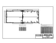
Printed Circuit Board<br />
I was <strong>for</strong>tunate to have an SSM2166S<br />
on hand, courtesy of Analog Devices, and<br />
this prompted me to start the prototype. I<br />
made an SMD to DIP adapter to allow me<br />
to use a solderless breadboard designed<br />
<strong>for</strong> DIP devices. After I had completed the<br />
PCB layout I discovered a source <strong>for</strong> the<br />
DIP package, the SSM2166P, 6 <strong>for</strong> which I<br />
completed a second version. Both versions of<br />
the PCB employ the manufacturer’s advice<br />
on star grounding and short lead lengths to<br />
minimize instability. Builders should get the<br />
desired chip be<strong>for</strong>e ordering one of the two<br />
versions of the PCB.<br />
I ordered prototype printed circuit boards<br />
from ExpressPCB. 7 I chose the most economical<br />
approach by ordering boards that<br />
are double sided with plated through holes<br />
but do not have a solder mask or component<br />
silk screening. Regardless of the manufacturer,<br />
groups of builders or clubs should get<br />
together and order the boards in quantities<br />
to reduce the cost. You can see the various<br />
cost breakdowns by installing the free PCB<br />
software and loading one of the layouts,<br />
<strong>VocalMaster</strong>-DIP.pcb or <strong>VocalMaster</strong>-SMD.<br />
pcb. If the PCB does not have plated-through<br />
holes, be sure to solder the components on<br />
both sides of the board. Additionally, if the<br />
pad is a feedthrough, insert a short length of<br />
wire and solder on both sides. The inside top<br />
view of the completed <strong>VocalMaster</strong> is shown<br />
in Figure 3. Check with the author to determine<br />
the availability of fabricated boards.<br />
Printed Circuit Assembly<br />
Install the components by referring to the<br />
printed circuit board (PCB) assembly drawing<br />
<strong>for</strong> part numbers and locations, and the<br />
materials list <strong>for</strong> corresponding values. For<br />
the DIP version, use a small soldering iron<br />
of 25 W or less with a standard small tip.<br />
For the SMD version, a very tiny tipped iron<br />
( 1 ⁄16 inch) and a magnifier are mandatory <strong>for</strong><br />
soldering the SSM2166P.<br />
A beginners guide to surface mount<br />
technology is a good starting point to get<br />
you acquainted with the tools and methods<br />
involved. 8 Work with plenty of light<br />
and use small gauge solder sparingly, as<br />
the PCB pads are small. Too much solder<br />
will increase the chance of a solder bridge,<br />
especially on boards without a solder mask.<br />
Cleaning the tip on a damp sponge be<strong>for</strong>e<br />
every solder joint will decrease the chances<br />
of a faulty connection. Although not mandatory,<br />
I encourage the use of IC sockets to<br />
aid in testing and troubleshooting. Observe<br />
polarity on all ICs, diodes and electrolytic<br />
capacitors. All components should be<br />
mounted close to the board to minimize lead<br />
lengths.<br />
Trimpot R19 will be adjusted following<br />
assembly to illuminate the red LED on audio<br />
peaks that produce distortion in the transmitted<br />
signal.<br />
Save the clipped ends of component<br />
wires <strong>for</strong> installing ferrite beads FB1-FB8.<br />
Install all components except U1, U2, U3<br />
and U4. Take your time and check your work.<br />
If your eyes are as bad as mine, a magnifying<br />
glass, headband or worklight may come<br />
in handy. When you are satisfied, connect<br />
MIC OUT to the radio microphone input with<br />
a short jumper cable. Attach the negative<br />
lead of a dc voltmeter to the PCB common<br />
connection. Turn on the radio, and, using the<br />
voltmeter positive lead, check <strong>for</strong> 5 ±0.2 V<br />
dc at the following locations: U1, pin 14; U2,<br />
pin 4; U3, pin 14, and U4, pin 3. If all voltages<br />
are okay, remove power and connect the<br />
mic to the MIC IN jack, J1. Place S1 in the OUT<br />
position and ensure that the radio is functioning<br />
normally, including the microphone<br />
audio, UP, DOWN and FAST functions. If you<br />
experience problems go back and inspect the<br />
PCB <strong>for</strong> incorrectly installed components,<br />
reversed polarities, solder bridges, and faulty<br />
solder joints. When the test is successful,<br />
remove power and install the ICs in their<br />
sockets. Pin 1 is identified with a square pad<br />
on the PCB. Make sure all pins are aligned<br />
be<strong>for</strong>e pressing them into the sockets or you<br />
may bend them.<br />
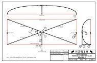
Enclosure<br />
Using rubber cement, secure the templates<br />
(see drawing sheet 3, www.arrl.org/<br />
files/qst-binaries/Baker0106.zip) and drill<br />
all holes on the front and rear panels. The<br />
rectangular holes on the rear panel will also<br />
require a file and some elbow grease to get<br />
them properly sized. To improve the appearance<br />
of the front panel holes, use a countersinking<br />
bit to lightly remove the rough<br />
edges. You may want to blacken the hole<br />
edges using an aluminum blacking solution,<br />
sold in gun stores. I used white enamel paint<br />
on the control indicator marks to make them<br />
more visible. Using a small jeweler’s screwdriver,<br />
dip the tip into the paint and touch<br />
the inside of the control slots. Use small<br />
amounts and allow the paint to flow only<br />
into the slot. Clean up using a cotton swab<br />
damped with paint thinner.<br />
Labeling was added using white dry<br />
transfer letters. Print a full size template<br />
onto clear film. Tape the panel to a flat<br />
surface and clean it with rubbing alcohol.<br />
Tape the top edge of the clear template over<br />
the panel. Insert the dry transfer sheet in<br />
between, line up each character under the<br />
template and burnish. I used 1 ⁄8, 3 ⁄32 and 1 ⁄16<br />
inch characters found in the HO railroad<br />
section of my local hobby shop. 9 Clean up<br />
with masking tape and cotton swabs moistened<br />
with alcohol. Seal the lettering by<br />
spraying on two light coats of clear lacquer<br />
or decal sealer. Figure 4 shows the details of<br />
the front panel lettering.<br />
It is important to note that the removable<br />
panel is located at the enclosure top. This is to<br />
allow access to R19 and to prevent the PCB<br />
traces from contacting the enclosure PCB<br />
mounting channels. Attach the front bezel