3.6M north10.pdf - Dean-O's Toy Box
3.6M north10.pdf - Dean-O's Toy Box
3.6M north10.pdf - Dean-O's Toy Box

Create successful ePaper yourself
Turn your PDF publications into a flip-book with our unique Google optimized e-Paper software.
10. Cathode Pulsers: Hard-Tube Modulators<br />
The hydrogen thyratron, the half-control device most commonly associated<br />
with the line-type pulser, is often simply called a “soft-tube” modulator because<br />
it is filled with low-pressure hydrogen. If the soft tube is filled with low-pressure<br />
hydrogen, what is a “hard” tube filled with? The answer is: as close to nothing<br />
as possible. In short, the tube is “filled” with as “hard” a vacuum as can be<br />
achieved and maintained, typically 10-8 to 10-9 torr. (Be assured that the external<br />
envelopes of both tube types are equally hard.)<br />
The fewer the number of residual gas molecules in a hard tube the better. A<br />
plasma arc in a soft tube is its conduction mechanism. Once the arc is initiated,<br />
however, it can be terminated only by means external to the tube, hence its “halfcontrol”<br />
designator. A plasma arc in a hard tube, on the other hand, is a fault<br />
condition. The conduction mechanism is the flight of free electrons from the<br />
cathode, or virtual cathode, to the anode. This mechanism is sometimes called<br />
space-charge-limited operation. (The charge carrier in this case is the cloud of<br />
electrons that hovers near the thermionic emitter.) Each electron that leaves the<br />
cathode must make it to the anode in order to contribute to useful load current.<br />
Therefore, any electron collision with residual gas molecules must be minimized.<br />
The number of electrons that are permitted to make the trip per unit of time<br />
and per unit of area is called current density. Current density is controlled by<br />
means of the voltage applied between the cathode and a helical or meshlike grid<br />
(or grids) positioned somewhere between the cathode and the anode. This grid<br />
or control electrode of whatever type is placed physically closer to the cathode<br />
than to the anode-usually much closer, so that the electric field produced at the<br />
surface of the cathode by voltage applied between grid and cathode will be<br />
proportionately greater than the field intensity produced by voltage applied between<br />
anode and cathode.<br />
10.1 The full-control switch tube<br />
A vacuum tube-or “valve” as the English insist on calling it—that has a<br />
cathode, an anode, and a control grid is called a triode. A tube with an additional<br />
grid located between the control grid and the anode is called a tetrode.<br />
(Other electrodes such as the suppressor grid in the pentode, the shield grid, and<br />
even an arc-shield electrode are sometimes employed in hard tubes. But the<br />
triode and the tetrode are the basic gridded-tube types.) Their geometries can be<br />
planar or coaxial. In the planar configuration, the cathode, grids, and anode take<br />
the form of circular discs. Jn the coaxial configuration, which is also referred to<br />
as a radial-beam tube, the electrodes take the form of coaxial cylinders, with the<br />
anode being either external or internal (either the outermost or innermost cylinder).<br />
In any case, the total current that leaves the cathode is shawd between the<br />
anode and the grid(s). The portion of the total current shared with the anode is<br />
considered the useful current. Even though grids are perforated so that electrons<br />
can pass through them, they are not electronically invisible. If the voltage ap-<br />
146
Cathode Pulsers: Hard-Tube Modulators (10) 147<br />
plied to a grid is positive with respect to the cathode, some electrons will be<br />
intercepted. (This is almost always true for the screen grid and, in a high-power<br />
gridded tube when full current is being demanded, for the control grid as well.)<br />
One of the goals of tube design is to minimize the control-electrode current<br />
because it serves no useful purpose and subtracts from the current that can be<br />
useful. The total cathode current in a tetrode can be expressed as:<br />
I =<br />
cathade I anode + lco.troIgrid + Is.reen grid = ‘:’<br />
where K is the effective perveance. K can also be evaluated as<br />
~= 2.33x 10+(A)c<br />
(Sdiade)’ ‘<br />
where A is the cathode emitting area in cmz, c is a constant dependent on tube<br />
geometry, S~l~e is the equivalent diode spacing and given in cm, and V is the<br />
effective voltage. The fractional exponent 3/2 applies to most tube geometries.<br />
Effective voltage can be further defined as<br />
v v<br />
v=Vcontro,tnd + ““en “d +J=-,<br />
where Psg and ~ are the amplification factors of the semen grid and anode,<br />
respectively.<br />
The perveance of electron tubes can vary from less than 10~ perv., or 1 ~perv<br />
(the equivalent to 1 pA/V3t2), for a high-performance millimeter-wave TWT, to<br />
0.01 perv, or 10,000 ppervs (the equivalent to 0.01 A/@JZ), for a large, gridded<br />
power tube. The screen-grid and anode amplification factors, or p~g and ~, are<br />
factors that quantify the strengths of the electric-field contributions at the cathode<br />
produced by voltages applied to screen grid and anode as they relate to the<br />
electric field produced by the control grid. If, for instance, a tetrode had a screen<br />
amplification factor of 10, it would require a change of screen-grid voltage 10<br />
times as great as that of the control grid to have the same effect on cathode<br />
current change. Similarly, if the anode amplification factor were 100, the change<br />
in anode voltage would have to be 100 times as great as the change in controlgrid<br />
voltage for the same cathode-current change. The screen-grid and anode-p<br />
factors reflect the facts that not only are the screen grid and anode farther away<br />
from the cathode than the control grid, but the field produced by voltage on the<br />
screen grid must penetrate the shielding effect of the control grid, and the field<br />
produced by voltage on the anode must penetrate the shielding effects of both<br />
grids. We can see, then, that for positive voltage applied to both screen grid and<br />
anode, there will be a negative voltage that, when applied to the control grid, will<br />
cancel the field-strength contributions of the others and result in no current leaving<br />
the cathode. This balance point is called the cut-off grid bias for a given<br />
Psg<br />
Pa
148 High-Power Microwave-Tube Transmitters<br />
Soft-tubs line-type modulstor<br />
Shun_thsrd-lube mcdulstor<br />
(topo!qical descendant of line-type moduhtor)<br />
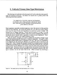
Figure 10-1. Progression of sofi-tube, line-type moduhtor into shunt-type, hard-tube modus’utor.<br />
combination of screen and anode voltages.<br />
Because of cut-off grid bias, the hard tube can be turned off as well as on.<br />
Tube current, therefore, can be fully controlled by the voltage applied to the<br />
control grid from zero to the maximum. (The maximum curxw-tt is determined<br />
by cathode emissive capability, a factor that varies with cathode area, cathode<br />
material, and cathode temperature.) This feature, then, makes the tube a “proportional<br />
and reciprocal” full-control modulator switch. It is called proportional<br />
and reciprocal because the factors that will reduce current are simply the reverse<br />
of the factors that can increase it. More will be said about hard-tube technology<br />
later.<br />
10.2 Hard-tube modulator topology<br />
Figure 10-1 shows how the replacement of the half-control switch in the linetype<br />
modulator with a full-control switch allows the pulse-forming network to<br />
be replaced with a quasi-infinite energy store. This is now possible because the<br />
time delay of an artificial transmission line is no longer required to externally<br />
turn the switch tube off through commutation. Initiated by a trigger, the pulse<br />
duration in the line-type modulator was set by network constants: the PRF was<br />
limited by the rate of rise of charging voltage across the soft switch tube, while<br />
the pulse-repetition interval (PRI) had to exceed<br />
The pulses of current removed from the hard-tube modulator are now replicas of<br />
the voltage applied to the grid of the hard switch tube. The output voltage V. of<br />
the hard-tube modulator is the inverted replica of the circuit’s switch tube grid<br />
drive voltage. Unlike the line-type modulator, the output-pulse duration and
Cathode Pulsers: Hard-Tube Modulators (10) 149<br />
[<br />
v,<br />
J.-.<br />
k<br />
.-. — -—-— ---<br />
t<br />
--l<br />
+<br />
A~O<br />
f<br />
Voltage change on cathode Iiiear with time<br />
“Semxfyne” or Doppler frequamcy shift<br />
f,il> b f,out<br />
Phase change through<br />
amplifier Iiinear with time<br />
Figure 10-2. Consequences ofpulse voltage decrement, or “droop,” on power and phase shift.<br />
PRF of the hard-tube modulator is versatile. On the other hand, the pulse-top<br />
ripple of the line-type modulator is replaced by the voltage decrement, DVV of<br />
the hard-tube modulator, but this condition can be compensated for by ramping<br />
the input. Changes in the terminal voltage of the energy-storage capacitor—<br />
especially the decrement, or “droop,” in voltage that any finite-sized capacitor<br />
will experience when a charge is removed from it-can be compensated for by<br />
the proportional property of the grid-voltage/plate-current transfer characteristic<br />
and the ability of the anode to dissipate significant pulse energy and continuous<br />
power.<br />
The capacitance Cs (for storage capacitance) for the hard-tube circuit is many<br />
times larger than CIV(for network capacitance) for the soft-tube circuit for a given<br />
amount of pulse energy because Cs is only partially discharged each pulse, whereas<br />
CM as we recall, is completely discharged with each pulse. Even though the loss<br />
in capacitor voltage experienced during a pulse can be compensated for by a<br />
complementary change in switch-tube anode voltage, as mentioned above, this is<br />
an energy- and power-wasteful process. To maximize the efficiency of a hardtube<br />
modulator-which, as we will see, will be difficult enough—the switch tube<br />
is typically driven to the minimum anode-voltage drop that is still consistent<br />
with the peak current required so that capacitor-voltage droop will be passed on<br />
the load voltage. How much droop is tolerable? The answer, of course, depends<br />
upon the nature of the microwave tube load. (Refer back to Fig. 9-28 for some<br />
idea.)<br />
Figure 10-2 shows the effect of incremental voltage change on pulse energy<br />
and phase angle. For a microwave tube having a linear-beam electron gun with<br />
space-charge-limited electron flow, beam power will vary as the 5/2 power of<br />
.bearn voltage. For a small value of AVo/VO,the loss in electron beam power, APB/<br />
PB, from the beginning to the end of the pulse will be 2.5AVo/Vo. The loss in perunit<br />
electron-beam pulse energy will be the time average of the power loss over<br />
the pulse, which, for small values, can be treated as linearly varying. This figure<br />
amounts to approximatelyhalf of the end-of-pulsepower loss, or 1.25AV0/VO.
150 High-Power Microwave-Tube Transmitters<br />
+V<br />
Vidao<br />
drive<br />
----<br />
-.-t -------<br />
+ ~ Crowbar<br />
@y!-<br />
. .<br />
c<br />
J<br />
t<br />
1 &<br />
video<br />
.<br />
-v 1<br />
@ ~<br />
A. Transfomsar-casplad, @fiva-suppfy, shunt switch C. Transformer-cwplad, nagativa-supply, sarias switch<br />
(crowbar and logic must float)<br />
(vidao driie refererwad to nagafive high wilage)<br />
B. Transfonrwwxuplad, posifiva-s@y, series switti<br />
(both Iow-side pulse-transformer tannds must ba insulated<br />
for high voltage)<br />
D. Diract-couplad, rwgatke-suppty, .serfes switch<br />
(sams as above, but switch must be salad forbad<br />
wlfaga)<br />
Figure 10-3. Alternative circuit arrangements for hard-tube modulators.<br />
For a crossed-field-type device, the effect of voltage change will be far more<br />
pronounced. In this case, APz#PB will be as much as llAVO/VO,and the approximate<br />
per-unit loss in pulse energy will be 5.5AVo/Vo. (These values refer only to<br />
loss of dc beam.) Other factors listed in Fig. 9-28 relate to how RF power output<br />
will be affected.<br />
Because beam-voltage change for small values of AV/V is very nearly linear<br />
with time, the change in RF phase angle between input and output of the RF<br />
amplifier tube will be nearly linear. (This was noted in the section that discussed<br />
phase-pushing effects.) However, linear phase change is indistinguishable from<br />
pure frequency translation: the frequency coming out is offset from the one going<br />
in. The amount of frequency difference is equal to the percentage of voltage<br />
change times the pha=pushing factor expressed in degrees per percentage of<br />
voltage change. To find the differential phase change over the duration of the<br />
pulse, this product is divided by the pulse duration, or At times 3600/cycle. In<br />
the TWT example shown, the phase-pushing factor is 40°\170AV/V, the voltage<br />
droop AV is lYo, the pulse duration is 1 ms (0.001 second). The frequency offset,<br />
A~(absolute, not per-unit), will therefore be<br />
l%x40°/1%<br />
360 X 0.001s<br />
=lllCYC<br />
/ ~=111<br />
Hz.
Cathode Pulsers: Hard-Tube Modulators (10) 151<br />
The phase slope with time is40,000°/s. -Because there are360° per cycle, the<br />
frequency shift, which is exactly the same as a Doppler shift, is 40,000/360, or 111<br />
Hz. This effect has been referred to by some as the “serrodyne” effect because of<br />
its serrated, or sawtooth, waveform, which is caused in this case by voltage<br />
removal from a capacitor. Before there were modern frequency synthesizers with<br />
phase-locked loops and other means of assuring phase coherency between transmitter<br />
and receiver local-oscillator frequencies, the serrodyne effect was actually<br />
used to achieve the frequency offset between them. This was done by applying a<br />
linear ramp of voltage with its short-duration reset timed so that the period of<br />
the resulting sawtooth waveform was the same as the desired receiver intermediate<br />
frequency. This sawtooth waveform was applied between helix and cathode<br />
of a low-power, continuous-wave TWT that had a relatively high phase-pushing<br />
factor. With proper adjustment of the amplitude of the sawtooth waveform, the<br />
RF output would be at the desired local-oscillator frequency.<br />
Figure 10-1 showed the most gradual of topological changes that could ease a<br />
designer from the line-type, half-control-switch modulator technology into the<br />
hard-tube, full-control-switch modulator technology. Figure 10-3 shows four further<br />
refinements. The first refinement, illustrated in Fig. 10-3a, simultaneously<br />
replaces the soft-tube switch with the hard-tube switch and the artificial transmission<br />
line PFN with a capacitor energy store, which is coupled with a series faultcurrent-limiting<br />
resistance. In the case of a switch-tube arc, however, all of the<br />
charge and energy stored in the capacitor will be dumped. Charge and energy<br />
will be transferred to the load connected to the puk+transformer secondary until<br />
the transformer core saturates, which, in a well-engin~md application, will not<br />
be much longer than the longest normal pulse. Up until this time, the cur~nt in<br />
the discharge loop will only be about 15!40 greater than the normal load current,<br />
assuming that the normal switch-tube voltage drop was approximately 10% of<br />
the initial capacitor voltage and that the load is a 3/2-power, space-charge-limited,<br />
diode-type electron gun.<br />
When the pulse transformer core saturates, the transfer of energy and charge<br />
to the load terminates, but things get much worse for the faulted switch tube.<br />
Remember from the discussion on half-control switches that an arc in vacuum is<br />
a very good conductor with almost negligible voltage drop. Current is now<br />
limited only by the series resistance of the capacitor. What is more, the action<br />
integral of the discharge, or<br />
J i2dt,<br />
is equal to the stored energy divided by the value of series resistance. (joules/<br />
ohm is the equivalent of ampere~seconds.) If the arc in the switch tube was<br />
between the &ode and one OFthe small-diameter wires that makeup the control<br />
grid, the action integral determines whether the grid wire will fuse. If it does<br />
and if enough grid wire is involved, the voltage on the grid will no longer<br />
effectively cut off anode current in the interpulse interval.<br />
For low intrapulse voltage droop, the capacitor’s stored energy should be
152 High-Power Microwave-Tube Transmitters<br />
many times the amount delivered to the load- over the course of the longest<br />
normal pulse. (Q = Cw so AV/V = AQIQ. For a 107’ovoltage droop, the stored<br />
charge must be 10 times charge delivered per pulse. For a 5’XOdroop, the stored<br />
charge must be 20 times charge per pulse. Because the load voltage, V, is almost<br />
constant, both stored and load energies are proportional to charge, W = QV.)<br />
With 10 to 20 times more energy stored in this type of modulator, a means of<br />
charge diversion from the faulted switch tube is often necessary. This is usually<br />
handled by an electronic crowbar. For physically and electrically large capacitive<br />
storage, the topology illustrated in Fig. 10-3a already suffers from the fact that<br />
both terminals of the storage system must not only float at high voltage but they<br />
must support rapid pulse-voltage change as well. When the added complexity of<br />
an electronic crowbar system is factored into this configuration, an alternative<br />
architecture becomes attractive.<br />
One advantage of the Fig. 10-3a topology is that the switch-tube grid drive<br />
and filament circuits are returned to ground. If we keep this advantage and<br />
reconnect the capacitor bank and crowbar so that they are also referenced to<br />
ground, the topology of Fig. 10-3b emerges. Although the storage terminals no<br />
longer float, both terminals of the pulse-transformer primary float. This means<br />
that during the interpulse interval both terminals must be insulated from the core<br />
for the power-supply voltage. This introduces the possibility of a failure mode in<br />
a component that should normally be one of the most reliable in the entire transmitter.<br />
Therefore, this is not a popular solution among those who make their<br />
livings designing and building transformers. For this reason, the arrangement<br />
shown in Fig. 1O-3Cis the most common.<br />
In Fig. 1O-3C the pulse-transformer primary and capacitor-bank/crowbar are<br />
referenced to ground, and the power-supply polarity is reversed. The switchtube<br />
drive and filament circuits are now referenced to the negative high voltage.<br />
The filament power supply for the switch tube, which is often no more than a<br />
step-down power transformer (albeit one that may be rated for kilowatts of heater<br />
power), must now also be insulated for the operating anode-cathode voltage of<br />
the switch tube. This is not, however, a high-performance requirement, in that<br />
leakage inductance and interwinding-.<br />
capacitance of the transformer are of little<br />
or no concern. What might, under other circumstances, be considered excessive<br />
leakage inductance can even be advantageous in this case, in that it will automatically<br />
limit cold-filament in-rush current. (The resistance of a switch-tube<br />
filament, like that of most wires, follows a positive temperature-coefficient characteristic,<br />
where resistance increases with temperatun+-except that the temperature<br />
of this wire will eventually reach about 1000”C.)<br />
The grid-drive circuits also will require primary power that is isolated from<br />
ground for the full anode-cathode operating voltage. This power is often derived<br />
from the isolated filament power (or vice versa). More important, the low-level<br />
gate, or on/off trigger signals, must also be coupled from ground-level reference<br />
to high-voltage deck reference. Modern designs rely almost exclusively on optically<br />
coupled links for this function, even though the common-mode rejection<br />
requirements are far less for this application than for the “floating-deck” type<br />
modulator, which will be discussed later. In this case, even though the reference<br />
deck is at high voltage with respect to ground, this voltage is relatively constant
Cathode Pulsers: Hard-Tube Modulators (10) 153<br />
with time. Any changes consist mostly of the capacitor-bank droop and the<br />
voltage drop across the surge-current-limiting resistors caused by the normal<br />
peak-load current. Before there were dependable high-performance optically<br />
coupled signal links, special pulse-transformer designs and even pulsed RF links<br />
were used to transmit low-level timing signals across the high-voltage gap, examples<br />
of which we will see later. As complicated as these circuits are, they are<br />
in most cases preferable to solving the problem of insulating the pulse-transformer<br />
primary winding for the full switch-tube operating voltag~specially<br />
because the performance of the pulse transformer is either the most important<br />
issue or second only to that of the switch tube itself.<br />
Circuit complications am also unavoidable in the final configuration, which<br />
is shown in Fig. 10-3d. This is the direct-drive hard-tube modulator—the top of<br />
the line, as it were. In this design, there is no pulse transformer at all. This<br />
feature eliminates the limitations on pulse duration, rise-and-fall times, intrapulse<br />
droop, and leading-edge overshoot &d ringing. The price paid for this imp~ovement<br />
is increased circuit complexity and the fact that the switch tube itself must<br />
handle the full operating voltage and current of the microwave tube load as<br />
separate and independent ratings-not as a peak-power product, where lack of<br />
voltage hold-off can be compensated for by increased current-handling (or viceversa)<br />
with any mismatch handled by an appropriate pulse-transformer turns<br />
ratio. This direct-drive connection is capable of the highest performance of all<br />
modulator types. Given enough excess capability, or head-room, it can be programmed<br />
to compensate for almost every shortcoming of the rest of a transmitter,<br />
including power-supply ripple, noise, and capacitor-bank droop. In fact,<br />
there is a class of switch tube, which will be described later, that will do much of<br />
this with no programming at all. Not surprisingly, therefore, this class of modu-<br />
I<br />
Figure 10-4. The back-swing clipper circuit as used with transformer-coupled unidirectional! [o&.
154 High-Power Microwave-Tube Transmitters<br />
later is almost always the most expensive, if not always the largest.<br />
Before leaving the high-power output-pulse transformer behind, it would be<br />
negligent not to discuss its use in a hard-tube modulator that has a diode-type, or<br />
unidirectional, conduction (de) load. We have already mentioned what can be<br />
done with energy stored in the transformer magnetizing inductance when used<br />
in a line-type modulator. So long as the switch tube is still in the forwardconduction<br />
state, the energy will manifest itself as reverse voltage on the pulseforming<br />
network. This is not possible in a hard-tube modulator, because the<br />
means of terminating a pulse is to stop switch-tube conduction. This situation<br />
leaves no place for the flow of current, which has built up in the magnetizing<br />
inductance over the course of the pulse. For this reason, a back-swing clipper<br />
circuit, as shown in Fig. 10-4, is required. Without it, the voltage across the<br />
transformer primaxy will jump up at the end of the pulse in a direction that<br />
increases the forward voltage across the switch tube (just as it is trying to recover<br />
its voltage-blocking state and after its electrodes have been heated to their maximum<br />
transient temperatures). The result will be a switch-tube arc. The clipper<br />
circuit provides a path for the magnetizing current after the switch tube is cut off.<br />
This clipper current can be defined as<br />
.<br />
‘clipper<br />
=<br />
J<br />
lMe-tRCILM – lbiLhf<br />
4’<br />
where RC is the clipper resistance, LM is the transformer magnetizing inductance,<br />
and lM is the peak value of magnetizing current that occurs at the end of the<br />
pulse of voltage applied to the transformer. The energy stored in the transformer<br />
magnetizing inductance, WM, can be defined as<br />
where Vp is the voltage pulse output of the switch tube and z is the pulse length.<br />
There will still be a transient overvoltage due to the clipper resistance in<br />
series with the clipper diode. Without series resistance, the clipper time-constant<br />
could theoretically be infinite because it is LM/Rc. The greater the value of Rc,<br />
the shorter the recovery time will be but the greater will be the peak reverse<br />
voltage. The volt-time products across a transformer winding must be equal in<br />
the positive-going and negative-going polarities. If they are not, the result is<br />
time-averaged voltage across the winding-which ultimately is just a length of<br />
wire-and it is difficult to maintain average voltage across it. The larger the<br />
value of clipper resistance, the shorter the decay time of magnetizing current but<br />
the greater the transient overvoltage, which is equal to IM x Rc. There can be an<br />
advantage to using a non-linear resistance such as Thyrite, or the more modern<br />
metal-oxide varistor (MOV), as the clipper load . A properly selected non-linear<br />
resistance will have nearly constant voltage across it throughout the interpulse<br />
interval, thus minimizing the stress on the switch tube immediately following the
Cathode Pulsers: Hard-Tube Modulators (10) 155<br />
pulse, which is the time when the tube is ieast able to handle it. The MOV clamp<br />
voltage should be chosen so that the product of it and the minimum interpulse<br />
interval is as close to the product of pulse voltage and pulse duration as possible,<br />
making positive- and negative-going volt-time products equal across the transformer<br />
winding.<br />
10.3 Storage capacitors<br />
We all know that a capacitor is a device that consists of no more than two<br />
plates separated by dielectric material and is capable of storing energy in the<br />
electrostatic field between the plates. Nevertheless, entire books have been written<br />
on capacitor technology. What a transmitter designer is most concerned with<br />
is what the ratings of a capacitor mean and how the stress levels imposed affect<br />
capacitor performance.<br />
Generally speaking, the factor most important in determining a capacitor’s<br />
volume and cost is the energy it is capable of storing. This assumes, however,<br />
that once a capacitor is charged, its repetitive discharges will only be partial.<br />
(This was clearly not the case with the capacitors used to store energy in the<br />
PFNs of the line-type modulators. These capacitors were completely discharged<br />
each pulse during normal operation.) In addition, under some fault conditions<br />
the voltage can be reversed across the capacitor, which is one of the most stressful<br />
events a capacitor can experienc+and this applies to capacitors that are not<br />
inherently polarized, such as electrolytic types. These caveats both hint at the<br />
fact that even though the energy stored in a hard-tube modulator capacitor bank<br />
might be 10 to 20 times that stored in the PFN capacitance for comparable pulse<br />
energy, we are not talking about the same kind of capacitors. Pulse-formingnetwork<br />
capacitors are high-stress components whose failure rates cannot be<br />
overlooked. (Water-cooling such capacitors is not unheard of, and most of them<br />
are more correctly rated in shot life or number of pulses in a lifetime rather than<br />
number of operating hours in a lifetime.)<br />
On the other hand, capacitors for partial-discharge, or de-filter, service are<br />
usually rated for a given operational life, which can be tens of thousands of<br />
hours at a given terminal voltage. They come in standard case sizes that differ in<br />
energy-storage capability. The height of their bushings also varies, depending on<br />
operating voltage independent of stored energy. These capacitors are expected to<br />
be operated at their rated voltages. The deratings for life expectancy which<br />
primarily affect voltage stress in the dielectric material, have already been designed<br />
in. Operating them at reduced voltage will, of course, result in great<br />
extension of life but at the expense of their stored energy,, which varies as the<br />
square of the voltage.<br />
However, these capacitors are no more tolerant of voltage reversal than any<br />
other kind. They will be fully discharged by a short-circuit load fault or by the<br />
operation of an electronic crowbar switch. It is extremely important that there be<br />
sufficient resistance in series with the discharge loop so that the discharge is<br />
critically, or overly, damped in order to preclude voltage reversal. This means<br />
that the series inductance of the loop cannot be ignored. In most cases, the value<br />
of series resistance will depend upon the permissible peak fault current and will<br />
be safely above the value required for critical damping,
156 High-Power Microwave-Tube Transmitters I<br />
r<br />
R=2 ;.<br />
But it is always prudent to calculate, or measure, the actual value of dischargeloop<br />
series inductance just to be sure. (This includes the internal series inductance<br />
of the capacitors themselves, which can vary depending upon how they are<br />
internally constructed.)<br />
In at least once case, an energy-storage system with a greatly undermatched<br />
artificial transmission line was used in lieu of a low-inductance capacitor bank<br />
having the same value of capacitance. In this design, characteristic impedance<br />
was 10% of the load impedance. The delay-time of the network was made equal<br />
to 1/2 of the longest pulse duration. The load—a super-power, long-pulse<br />
klystron— was connected in series with a hard-tube modulator switch, much like<br />
the one shown in Fig. 10-3d. When the modulator switch was gated on to initiate<br />
a pulse of load current, there was an instantaneous drop in network voltage of<br />
approximately 0.1 V, where V is the initial voltage across the network. The voltage<br />
across the klystron and modulator-switch combination was 0.9V. This voltage<br />
would persist for a time of 2T, where T is the delay-time of the network. At<br />
2T, the voltage would drop again by an additional O.IV, to 0.8V. If, however, the<br />
modulator switch tube was turned off after time T but before time 2T had elapsed,<br />
most of the network would have been discharged by an amount 0.2V, but not all<br />
of it.<br />
The load current was 0.9 V/R, where R is the effective resistance of the klystron<br />
in series with the conducting-state switch tube. If the storage system used the<br />
same value of capacitance but only the minimum-achievable value of inductance,<br />
the terminal voltage of the bank would start to droop in essentially linear fashion<br />
from the beginning of the current pulse to the end. If the starting voltage is V<br />
and the initial load current was V/R, the total droop would equal to the charge<br />
removed divided by the total capacitance, or AV = IAt/C. (This discussion is<br />
simplified by assuming that current is constant throughout the pulse, which it<br />
isn’t.) The time increment, tit, is the pulse length, 2T, which was the same as<br />
d(LC). The total load resistance was 10ZO, where Zo was the characteristic impedance<br />
of the network described above, or d(L/C). So R = 10~(L/C) and ~(L/C) =<br />
O.lR. Combining things,<br />
Av=<br />
r<br />
IAt ~x2@ 1X2 L ~x2xolR=02v<br />
-F ‘R C= R~= R”” ‘<br />
which was the same as the end-of-pulse step from the distributed network described<br />
above. The charge and energy removed from the capacitance was the<br />
same in both cases, except the finite-ZO network voltage changes in stair-step<br />
fashion while the minimurn-ZO capacitor bank changes in continuous ramp fashion.<br />
The purpose for creating this artificial network was to minimize the anode<br />
dissipation of the modulator switch because the source voltage was constant<br />
throughout the duration of the pulse, at 0.9V. In order to produce a flat-top load
Cathode Pulsers: Hard-Tube Modulators (10) 157<br />
voltage pulse in the latter case, the ramplike~ or droop, component would have to<br />
be subtracted from the output. To keep klystron voltage constant at 0.8V, the<br />
switch-tube anode voltage would vary from 0.2V at the beginning of the pulse to<br />
a theoretical minimum of zero (assuming no head-room requirement). The additional<br />
anode dissipation per pulse would be O.lV x 1, where O.lV is the timeaveraged<br />
anode drop and 1 was the load current, as before.<br />
This may have sounded like a good idea, but it wasn’t. Its fatal flaw was that<br />
it didn’t account for what happens under the major fault condition: simultaneous<br />
klystron and switch-tube arc-breakdown, or load shoot-through. The only<br />
good news was that the fault current was limited by the network characteristic<br />
impedance to 10 times 1, where I is the normal peak load current. Without series<br />
resistance, however, the network stored energy would tend to oscillate back and<br />
forth, completely reversing the voltage on the network capacitance periodically<br />
until the load arc was finally extinguished. To completely absorb network energy<br />
without capacitor-voltage reversal, a series resistance equal to ZO, or O.lR,<br />
was required between network and load. But this completely subverted the<br />
reason for the network in the first place. (This is but another example of having<br />
to design for the worst-case scenario rather than the hoped-for “normal” operating<br />
conditions.)<br />
Rarely if ever, are the capacitive energy-storage requirements of even a modest-sized<br />
transmitter met by a single capacitor (or “can,” as it is sometimes called).<br />
Multiple cans connected in parallel or series-parallel are the rule rather than the<br />
exception. The danger in multiple-capacitor arrays is what can happen if a single<br />
capacitor internally short circuits. If the total surge-current-limiting resistance is<br />
distributed throughout the array by having at least one resistor capable of dissipating<br />
the energy stored in a capacitor in series with each capacitor, a shortcircuit<br />
failure will cause no damage because virtually no energy will be dissipated<br />
in the faulted capacitor. Such an arrangement is so fault tolerant that the<br />
failed capacitor may not immediately reveal itself. (If the capacitors are all in<br />
parallel, the resistor in series with the failed capacitor will be connected across<br />
the dc power supply when an attempt is made to turn it on again. What is left of<br />
that resistor will usually bean adequate tell-tale sign for where the trouble lies.)<br />
Series-parallel connections are often employed when the system’s operating<br />
voltage is much above 50 kV. This is because energy storage density tends to<br />
degrade at much higher voltage, and more volumetrically efficient banks can be<br />
assembled from capacitors rated at less than 50 kV—by no means a hard and fast<br />
number-than those rated at, say, 100 kV. (In fact, probably the most volumetrically<br />
efficient energy storage bank assembled for 100kV-plus operation used a<br />
multitude of electrolytic capacitors that were individually rated at 450 Vdc. They<br />
were assembled in over 200 series-connected tiers and protected from individual<br />
overvoltage by a string of Zener diodes shunting them.) When there is a large<br />
number of series-connected tiers-say, at least five-the presence of a shorted<br />
capacitor in one tier will be far from obvious, even though it will short-circuit all<br />
of the parallel-connected capacitors in that tier through its series resistor. This<br />
short will cause the overall bank capacitance to increase, but all of the remaining<br />
capacitors will be subjected to 2570 overvoltage, or less, at the operating voltage.<br />
For this reason, some capacitor banks are interconnected with fusible links in-
158 High-Power Microwave-Tube Transmitters<br />
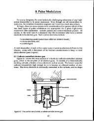
Figure 10-5. Typical series/parallel capacitor bank (two groups of 25 parallel-connected capacitors)<br />
totalling 70 /./.F,with triggered air-gap crowbar switches inforeground.<br />
stead of individual series resistors. Fusible links have the advantage of automatically<br />
disconnecting a failed capacitor. The fuse, however, must be of the type<br />
that permits very little let-through ener~, meaning that it must be arc-quenching.<br />
A capacitor subjected to too much let-through energy is likely to see its can<br />
rupture or its bushing explosively expelled-a spectacular but very hazardous<br />
event. When a capacitor bank has only two tiers, the effect of an individual<br />
shorted capacitor is the most easily observable, but the penalty for not observing<br />
it is the greatest the possibility of a 10094oovervoltage of the remaining tier. The<br />
voltage rating of a capacitor is associated with life expectancy more than external<br />
arc-over, and many high-voltage capacitors will endure 100!4o overvoltage for a<br />
short time. With only two or three tiers to the bank, it is advisable to measure<br />
voltage balance between tiers continuously and provide this information to the<br />
high-voltage dc interlock system of the transmitter.<br />
Stacked, multi-tiered capacitor banks also require corona shielding. A capacitor<br />
designed to operate at 50 kV may (or may not) have can and bushing geometries<br />
shaped so as to be corona-free (see Chapter 7 ). The capacitor cans of the<br />
first tier will typically be connected to the high-voltage return bus, the highvoltage-system<br />
“neutral,” which will be at or very near ground potential. The<br />
cans of the capacitors in the next tier will be at 50 kV with respect to ground, and<br />
their high-voltage-bushing terminals will be at 100 kV with respect to ground,<br />
■
Cathode Pulsers: Hard-Tube Modulators (10) 159<br />
and so on up the stack. The radii of curvature that are required for corona-free<br />
operation continually increase, but the capacitor can and bushing geometries do<br />
not, because most practical banks are built up of identical capacitors. Capacitors,<br />
therefore, are usually mounted on “rafts” that are surrounded by oblong, donutshaped<br />
corona shields whose cross-sectional diameters increase as the rafts ascend<br />
in height and voltage. An example of such construction is shown in Fig. 10-<br />
5. Please note that if spacings between conductors are adequate, very little shielding<br />
is required to prevent voltage breakdown. This is because corona under<br />
these conditions is self-healing; the exterior of the ionization sheath tends to<br />
expand so as to have the same effect as a large radius-of-curvature surface. However,<br />
in today’s sophisticated systems, which involve ever-more-sensitive and<br />
susceptible low-level circuitry, the electrical noise resulting from the corona dis-<br />
2.0<br />
1.8<br />
1.6<br />
1.4<br />
from power SUPPV<br />
1.2<br />
i<br />
*<br />
g 1.0<br />
~<br />
r!!<br />
0.8<br />
Energy dissipated<br />
0.6<br />
0.4<br />
0.2<br />
0.0<br />
0.0 0.2 0.4 0.6 0.8 1.0 12<br />
Per-unit capacitor discharge ~<br />
Figure 10-6. Capacitorchargingenergyrelationshipsas afimction of amountof capacitor discharge.
160 High-Power Microwave-Tube Transmitters<br />
charge is increasingly intolerable. (Remember what we used to pick up on the<br />
AM car radio when we drove near high-tension wires, especially on a foggy<br />
day?)<br />
We have discussed the fact that the removal of charge from a capacitor bank,<br />
no matter how large, will result in its terminal voltage being smaller than it was<br />
before the charge-removal interval, or pulse. In the interpulse interval, therefore,<br />
it will be necessary to replace the charge removed during the pulse. In the<br />
discussion of line-type modulators, much was made of the issue of recharging<br />
without incurring energy loss if the current was limited by resistance. Is there a<br />
similar concern when it comes to replacing partial discharge? The answer is not<br />
nearly as much. The reason for this is shown graphically in Fig. 10-6, which plots<br />
energy removed from the dc power supply, energy transferred to the capacitor<br />
bank, and energy dissipated in series resistance versus the per-unit amount that<br />
the capacitor is discharged each pulse. (This graph assumes that the resistance is<br />
small enough so that the RC time-constant is less than approximately 1/3 of the<br />
minimum interpulse interval, assuring that the capacitor will recharge to approximately<br />
the power-supply terminal voltage between pulses.) If we look at<br />
full discharge, or per-unit discharge of unity, the results are familiar. The perunit<br />
capacitor energy transfer and resistor energy dissipation are both unity, and<br />
the per-unit energy removed from the power supply is 2. Notice, however, that<br />
only the energy removed from the power supply is a linear function of per-unit<br />
discharge voltage. For less-than-unity per-unit discharge, energy transferred to<br />
the capacitor falls off less rapidly than dissipation in the resistor. Therefore, the<br />
efficiency of energy transfer increases as AV/Vdecreases.<br />
The reason for this can be seen if we note the change in charge during a pulse<br />
of current, AQ = CAV, and the change in capacitor energy, AW = AQ, times average<br />
capacitor voltage during discharge, which can be expressed as<br />
~Avx<br />
V+ V–AV<br />
2<br />
or<br />
~vAv _ C(AV)2<br />
The energy removed from the power supply during recharge is AQ times the<br />
power supply voltage, which can be expressed as CAV x V. Recharging efficiency<br />
is the ratio of energy transferred to the capacitor to the energy removed from the<br />
power supply, or<br />
2“<br />
+Av-a=,<br />
——— l[AV)<br />
CVAV 2V”
Cathode Pulsers Hard-Tube Modulators (10) 161<br />
When AVIV = 1, full discharge efficiency is 1/2, which we knew. For small perunit<br />
discharge-say, 0.1, or 107o droop+fficiency is 1- 1/2x 0.1 = 1-0.05 = 0.95,<br />
or 9570.<br />
In most high-power applications, however, resistance is not used between<br />
power supply and capacitor bank. Recharging current from the power supply is<br />
always limited by the equivalent ac series impedance of the power supply, most<br />
of which is the leakage reactance of the inductively coupled components, especially<br />
the high-voltage rectifier transformer.<br />
1.0<br />
I<br />
I 1 1 1 11111 A<br />
I I I I I IIIYI 1 I II 1 I 1 I I ml<br />
I<br />
10.4 Vacuum tubes as switch tubes<br />
Power grid vacuum tubes have numerous characteristics that define their<br />
total performance capabilities as pulse-modulator switching devices. The first<br />
characteristic of importance is peak-pulse power output, which is the product of<br />
the simultaneous maxima of load voltage and current that can be switched. Of<br />
course, the maximum load voltage is related to the continuous voltage that can<br />
be applied between anode and cathode of the tube while maintaining an accepta<br />
j = 0.5 Ncllf<br />
bj=l.olkn?<br />
cj=2.OA/cr#<br />
dj=5.o/VctTf<br />
e j= 10.ONW<br />
.01<br />
10 100 lC03<br />
Effecliv13peak drive voltage<br />
Figure 10-7. How cathode emission density is affected by spacing between grid and cathode (effect on<br />
perveance).
162 High-Power Microwave-Tube Transmitters<br />
screen)<br />
Virlusl Cathods<br />
‘ Real cathode<br />
Figure 10-8. How current density in region between anode and outermost grid is affected by the spacing<br />
between thent and effective drive voltage, due to the creation of a virtual cathode between the electrodes.<br />
ably low spark-down rate. Already it is obvious that there will be a degree of<br />
flexibility in what the usable anode hold-off voltage really is. In an application<br />
where a switch-tube arc is tantamount to disaster, an extremely conservative<br />
value must be used that will probably be even less than the manufacturer’s<br />
suggested operating voltage. Even this number is already somewhat less than<br />
the “absolute-maximum independent rating,” which defines voltage-hold-off capability<br />
at essentially no plate current.<br />
The useful load voltage is affected by load current as well. Maximum load<br />
current depends upon the type of cathode, its surface area, and temperature,<br />
which is related to heating power; and the current split between anode and other<br />
electrodes, such as the grid, shield grid, and semen grid. Although basic cathode<br />
research is ongoing and types capable of sustaining high emission densities over<br />
long lifetimes have come forth, power-grid-tube cathodes are still of two basic<br />
types: thoriated tungsten (directly heated) or oxide-coated (unipotential, or indirectly<br />
heated). (Million-hour emission lifetimes can at least be projected from<br />
today’s data bases for dispenser-type cathodes.) As current from the cathode<br />
increases, so must the minimum voltage between anode and outermost grid in<br />
order to avoid formation of a “virtual cathode” in the space between the two.<br />
Such an occurrence would prevent the passage of electrons through the region.<br />
(The electrons will not even leave the cathode unless there is adequate effective<br />
drive voltage.)<br />
Figure 10-7 relates cathode emission density to grid-cathode spacing and effective<br />
drive voltage. (The last parameter includes the contributions of anode,<br />
screen, and control-grid voltages as they are weighted by their respective amplification<br />
factors.) Figure 10-8 shows how the current density in the region between<br />
the outermost grid and anode is affected by drive voltage and spacing<br />
between the anode and outermost grid. These relationships can be defined by<br />
the equation<br />
\
Cathode Pulserw Hard-Tube Modulators (10) 163<br />
2.33 X 10”(~~~<br />
j. = ~2 7<br />
where j. is the density of current that can traverse the region between the outermost<br />
grid and anode, VAis the voltage between anode and cathode, VG is the<br />
voltage between grid and cathode, and d is the spacing between the outermost<br />
grid and anode. Notice that the useful component of current that travels from<br />
the grid to the anode is inversely proportional to the square of the distance<br />
between them.<br />
Figure 10-9 shows why this is not good news. The figure relates anode-grid<br />
hold-off voltage to the spacing between them. The uppermost plotted line, A, is<br />
the plane-parallel conductor experimental data, which is of mostly academic<br />
interest. Note the intercept at 100 kV for l-cm spacing. The 100 kV/cm gradient<br />
is often cited as a criterion for peak electric field in electron guns that use smooth<br />
copper surfaces, such as the ones for large klystrons. (An electric field of 100 kV<br />
at 1 cm may sound like a lot, but it is only about three times as great as the<br />
corresponding number for the dielectric strength of air at sea level. The actual<br />
geometries of power gridded tubes behave in less predictable fashion.) Getting<br />
back to Fig. 10-9, element B is a region rather than a line. It defines what one<br />
1<br />
I<br />
. t 1 1 1 1 1<br />
.<br />
I<br />
Hilf<br />
1$<br />
Curve A’: Plane parallel electrodes, e varies as (P’4<br />
. b<br />
Cwve & ForThW tubes with wire grid<br />
.<br />
Curve C<br />
For oxide cathode tubes with wire grid<br />
I<br />
I<br />
I<br />
0.1 1.0 10<br />
d –<br />
Electrode spacing (cm)<br />
“Experimental data by Kilpatric+i,RSI, Od. 1957<br />
Figure 10-9, Voltageltold-o~betweenelectrodesin vacuummfinctions of spacing and surface quality.
164 High-Power Microwave-Tube Transmitters<br />
I<br />
\<br />
r-’<br />
1-<br />
Figure 1O-10. Typical directly heated thoriated-tungsten wire-type cathode for power-gti tube.<br />
might expect for a tube with a wire grid and thoriated-tungsten (ThW) cathode.<br />
Region C defines the performance to be expected if the cathode is oxide-coated<br />
rather than thoriated tungsten. Oxide cathodes are, quite literally flakier than<br />
ones made of thoriated tungsten, and the products of surface deterioration can<br />
contaminate the grid wire, producing localized electric field enhancement. Tubes<br />
with higher p factors have more grid wires that are closer to the cathode so that<br />
the wire mesh functions more like an equipotential surface rather than individual<br />
wires with respect to the electric-field-strength enhancement produced by conductors<br />
of small radius-of-curvature. Smoothness of the wire is also important,<br />
but once an arc of sufficient action has terminated on a grid (or screen) wire, that<br />
wire, even if it is still there, will no longer be smooth.<br />
If oxide-coated cathodes perform less well with respect to high-voltage holdoff,<br />
why are they used at all? The reason is that thoriated-tungsten cathodes are<br />
not as efficient emitters with respect to heater power. For example, on a thoriatedtungsten<br />
cathode, one ampere of peak emission requires more than 15 W of<br />
heater power— and this is if a highly regulated filament voltage is used to precludetemperature-limited<br />
operation. (Pure tungsten filaments, on the other hand,<br />
are often deliberately operated in a temperatme-limited fashion in current-control<br />
diodes, where current is determined by filament power rather than anodecathode<br />
voltage). There is no pulse-duration limitation for such cathodes.<br />
A comparable oxide-coated cathode may require less than 1/3 as much heater<br />
power for the same emission current, but pulse durations are limited to tens of
Cathode Pulsers: Hard-Tube Modulators (10) 165<br />
.— .—<br />
MRbl<br />
Figure 10-11. Typical helical wire-type control gndfor high-power triode vacuum tube.<br />
microseconds and duty factors to 1% or less, which is more than adequate for<br />
many applications. Useful emission density for both types is 2 to 3 A/cm2. Even<br />
though emission from an oxide cathode can be 10 to 50 times this great for<br />
microsecond-length pulses, the only current that matters is what can get from<br />
outermost grid to anode. This current is limited by the virtual-cathode effect<br />
mentioned earlier.<br />
The thoriated-tungsten filament can be expected to last more than 10,000<br />
hours (or one year of continuous operation). This longevity is comparable to the<br />
life expectancy of the rest of the equipment if utilization is sporadic. The life<br />
expectancy of oxide-coated cathodes depends on too many factors to be accurately<br />
predicted or even repeated, but it is typically less than half that of thoriatedtungsten.<br />
Figure 10-10 shows how a directly heated thoriated-tungsten wire cathode for<br />
a high-power gridded tube is arranged. Such structures can become quite tall,<br />
and, when excited with ac heater power, can vibrate like tuning forks due to<br />
magnetic force caused by the filament current. Such filaments may require dc or<br />
high-frequency ac in order to produce no unbalanced magnetic force. (Or, as we<br />
will see later, such filaments may actually be built in three symmetrical sections<br />
in order to be excited with balanced 3-phase at.)<br />
Figure 10-11 shows what a similar tube looks like after a helical grid has been<br />
wound around the cathode wires. The closer the grid is to the cathode, the
166 High-Power Microwave-Tube Transmitters<br />
higher the p factor will be, the higher the cathode-current-density change will be<br />
for a given grid-voltage change, and the greater the anode-voltage hold-off is<br />
likely to be. The wire-to-wire spacing of the grid, however, will have to be<br />
smaller, approximately equal to the spacing between grid and cathode. This is<br />
done so the “screening” effect of the grid, or the amount of total grid area that is<br />
physically blocked by the presence of grid wire, will be greater than that of a<br />
lower-p grid spaced farther away from the cathode. The greater the screening<br />
effect, the more likely the grid is to intercept electrons on their way from cathode<br />
to anode when the grid is driven positive with respect to the cathode. This<br />
screening effect is reduced if the diameter of the grid wire can be reduced. But<br />
the diameter must still be large enough to dissipate heat, including the heating<br />
caused by its proximity to the hot cathode and the interception of electrons.<br />
Even more importantly the wire must have cross-sectional area (or AWG gauge)<br />
sufficient to absorb the action content of an arc discharge without fusing. (As<br />
will be discussed later, the transmitter designer is responsible for limiting the arc<br />
action by employing surge-limiting resistance and, when needed, an electronic<br />
crowbar charge diverter.) Even in high-p tubes, the grid screening factor is less<br />
than 259’0, and it typically varies down to 109’o for low-p tubes. Grid current at<br />
anode-saturation voltage is typically 1.5 times the screening factor, so that a 2570-<br />
screened, high-p triode may intercept grid current that is 1.5 times 259’o, or 389’o,<br />
of cathode current, compared with 1.5 times 107o, or 15?40,for a low+. triode.<br />
Grids are almost always wound of tungsten or molybdenum wim that has<br />
been coated with gold or platinum. This is done so they can operate at temperatures<br />
higher than the cathode-even as high as 1400°C (compared to 1000”C for<br />
the cathode)—without becoming primary emitters of electrons themselves. When<br />
they are driven positive with respect to the cathode they will attract and intercept<br />
electrons. The sum total of these electrons constitutes grid current, and the<br />
product of this current and the peak-grid voltage is the peak-grid dissipation.<br />
This current and power must be supplied by the external grid-drive circuitry and<br />
must be dissipated by the grid as heat.<br />
Because of an effect called secondary emission, not all electrons that collide<br />
with the grid are counted as grid current, however. Primary electrons strike the<br />
grid surface and knock off others, which continue onto the anode. So long as the<br />
secondary emission is less than the primary interception, things look good for<br />
both the tube and driver. On the other hand, if more secondary electrons are<br />
emitted than primaries are collected, grid current is negative and the grid can run<br />
away, unless it is externally swamped by shunt resistance. Pulse stretching is the<br />
usual symptom of excessive secondary emission; cathode and plate currents continue<br />
even after the grid drive pulse has stopped. Pulse stretching in some<br />
thoriated-tungsten tubes can be corrected by a process called grid blackening. In<br />
this process, filament voltage is increased to twice its normal value (so filament<br />
power approximately trebles). Some of the filament carburization boils off and is<br />
deposited on the grid, making its surface stickier and less prone to secondary<br />
emission. Secondary emission is less likely from grid wires whose surfaces have<br />
been made intentionally rough, but anode-voltage hold-off is degraded as a consequence.<br />
Recently manufactures have made grids and screens of pyrolytic graphite.<br />
This material does not emit secondary electrons, but tubes using it do not always
Cathode Pulsers: Hard-Tube Modulators (10) 167<br />
please their users because net grid current isalways higher forthem than conventional<br />
grids. Higher current means that grid drive circuits and screen-grid<br />
power supplies have to be rated for more output current. Nevertheless, with<br />
pyrolytic-graphite grids and screens there is less likelihood of tube-to-tube variations,<br />
or variations within a single tube over its life span.<br />
In oxide-cathode tubes, pulse duration is limited by the cathode. In thoriatedtungsten<br />
tubes, pulse duration is usually limited by intrapulse grid heating, which,<br />
ignoring heat lost by radiation, is adiabatic, meaning that no heat is dissipated<br />
during the pulse itself. Therefore, the temperature rise is proportional to the<br />
pulse energy, which is the product of peak power and pulse duration, and inversely<br />
proportional to the product of grid-wire mass and specific heat. If power<br />
is expressed in watts, pulse length in seconds, and mass in grams, the proportionality<br />
constant for temperature rise in degrees Celsius is 0.24. With grid temperature<br />
at 1400°C, however, radiation losses are fortunately not insignificant.<br />
The last electrode of a power grid tube is, of course, the anode, which is<br />
where we would like the majority of our cathode-emitted electrons to end up. A<br />
tube designer wants the electrons to arrive at the anode with a kinetic energy that<br />
is as small as possible relative to the anode area and the spacing between anode<br />
and outermost grid. This kinetic energy and the rate of electron arrival-which<br />
is, of course, the anode current-determine the anode dissipation. Only so much<br />
can be done to minimize it, and a conduction-anode drop that is 10?4oof the<br />
anode hold-off voltage is considered a good design, resulting in 90% anode efficiency<br />
as a modulator switch. The bulk of anode design, other than geometric<br />
requirements, falls in the category of heat transfer, which will be touched upon in<br />
a later section.<br />
Needless to say, grid and/or screen current does no one any good, and tube<br />
designers have exercised a great deal of their creativity in minimizing it. Now<br />
we will look at a few actual tube designs to see what has been accomplished in<br />
this regard. (Remember, of course, that almost nothing new has been done in this<br />
field for almost 30 years.)<br />
10.4.1 The 7560 triode switch tube<br />
Figure 10-12 shows the plate (anode) current characteristics for the 7560 triode<br />
modulator switch tube, which once was simultaneously manufactured by three<br />
of the largest and most competent power-vacuum-tube sources in the world.<br />
Today it may not be made by anyone, because two of the three have ceased<br />
operations and the third may no longer be interested. Nevertheless, there is still<br />
a host of operating sockets for the tube type, and shops that can rebuild it still<br />
flourish. The figure also shows the characteristics of another power triode, the<br />
8547, which is not primarily a modulator switch tube because its nominal anodevoltage<br />
rating is 17 kV. Both tubes have water-cooled anodes capable of dissipating<br />
175 kW of power. The 7560 differs from the 8547 only in the increased<br />
spacing between its anode and grid, which is required to achieve its 50-kV anode-voltage<br />
hold-off rating. Because the anode is farther away from the grid in<br />
the 7560, a designer would expect that greater grid-anode voltage drop would be<br />
required for a given amount of anode current given its virtual-cathode effect.<br />
Indeed, the effect is clearly illustrated in Fig. 10-12a by the slope of the “diode
168 High-Power Microwave-Tube Transmitters<br />
500<br />
A. Type 76W triotle B. Type 6547 Mode<br />
500<br />
I<br />
400<br />
400<br />
r<br />
I w F , ,<br />
I I I A I I<br />
100 I<br />
100<br />
I 1 /1 1 , , 1 1<br />
0<br />
0<br />
01 234_56789 io 012345678 9<br />
Plate voltage (l(V)<br />
Peak current (A)<br />
Figure 10-12. Voltagdcurrent characteristics for two power triodes: type 7560 (lefi) and type 8547 (right),<br />
which dt~er only in that the 7560 anode is fartherfiom its grid.<br />
line,” which is the line (not exactly straight) that slopes upward and to the right<br />
from the origin. It is also the line where all of the anode current lines merge.<br />
This diode line quantifies the virtual cathode and has a much steeper slope in the<br />
closely spaced electrodes of the 8547 than in the widely spaced ones of the 7560.<br />
If we select operating points for both tubes that meet the arbitrary but sensible<br />
90%-anode-efficiency criterion-at which the average output power could<br />
conceivably be as high as 175 kW/O.1, or 1.75 MW-we can determine how well<br />
grid current is managed in the two tubes. For the 7560, the conduction drop<br />
selected is 5 kV, which is 107o of 50 kV, and for the 8547 it is 1.7 kV, 107o of 17 kV.<br />
With positive grid voltage of 2000 V, the anode current of the 7560 is 380 A, and<br />
its grid current is 130 A. Therefore, the ratio of the two values is 2.10. Of the<br />
total 513-A cathode current, which is the sum of anode and grid currents, 7470<br />
became anode current and 2670 became grid current. This breakdown suggests a<br />
grid-screening fraction of 179’0, which would put the 7560 in the medium-p category.<br />
(Its p, in fact, is 45.) With 50 kV between anode and cathode, the grid<br />
must be negative with respect to cathode by approximately 1.1 kV for “projected”<br />
plate-current cutoff. (The actual plate-current cutoff requires an additional<br />
safety factor of negative grid bias.) The 8547, with a positive grid voltage<br />
of 2000 V, an anode current of 390 A, and a grid current of 100 A, has a ratio of<br />
3.10. Of the 490-A cathode current, 80~0 made it to the anode, and 2070 to the<br />
grid, suggesting a 13’70 grid-screening factor and lower p.. We know, however,<br />
that the tubes are identical except for anode-grid spacing, so the grid-screening<br />
factors are the same. The y is lower, however, because the anode is closer to the<br />
cathode (p.= 14).
Cathode Pulsers: Hard-Tube Modulators (10) 169<br />
8<br />
A Average-Plate Characteristics<br />
ma<br />
+3500 I<br />
400<br />
200<br />
100<br />
0<br />
b<br />
&<br />
1<br />
0 1 2 3 4 5 6 7“4” 8 9 10<br />
Plate voltage (k~<br />
B: Average Grid Characteristics<br />
150<br />
Rated filament conditions<br />
120<br />
90<br />
60<br />
Gnd volts= +2000<br />
3)<br />
+15W<br />
o<br />
o<br />
~ ‘:<br />
1 2 3 4 5<br />
Plale voltage (k~<br />
Figure 10-13. Vo@yYcurrentcharacteristicsfor the type8461triode.<br />
. .<br />
6<br />
I 8 9 10
170 High-Power Microwave-Tube Transmitters<br />
The filaments of both tubes operate at 14.5 V and 450 A, or 6250 W. At the<br />
rate of 15 W per cathode peak ampere, the available cathode current should be<br />
435 A. The actual peak-cathode current rating is 550 A. Although the 8547 more<br />
efficiently converts cathode current to useful anode current, its peak-pulse output<br />
power under the conditions evaluated is 6 MW, whereas the peak power<br />
from the 7560 is almost 20 MW. Neither of these tubes employs any special<br />
strategy, either geometric or electromagnetic, to minimize grid current. The grid<br />
is no more sophisticated than a helix of wire wound around the array of cathode<br />
wires.<br />
10.4.2. The WL-8461 triode switch tube<br />
This is another example of a thoriated-tungsten cathode. The WL-8461 is a<br />
“big but simple” power-grid triode modulator switch tube. Many sockets throughout<br />
the world are also filled with this tube, but it is no longer being manufactured.<br />
It is, however, being successfully rebuilt.<br />
The WL-8461 is ‘%ig” in that its anode-voltage hold-off rating is 75 kV, its<br />
peak cathode-current rating is 750A, and its water-cooled anode-dissipation rating<br />
is 200 kW. It is “simple” in that nothing special was designed into this tube<br />
to minimize grid current. Figure 10-13 shows its anode- and grid-current characteristic<br />
curves. Using the same 90%-anode-efficiency criterion (which yields a<br />
conduction-anode drop of 7.5 kV) and a positive grid voltage of 3.5 kV, the anode<br />
and grid currents are 600 A and 92 A, respectively, for a total cathode current of<br />
692 A. The current ratio, therefore, is 6.5. Anode current is 8870 of cathode current<br />
and grid current 1270 of it. These values suggest a low p. (Its p is actually 25,<br />
which is somewhat low.) In Fig. 10-13a, note the cross-hatched area in the anode<br />
(plate) current characteristics just to the right of the virtual-cathode diode line.<br />
This cross-hatch area is bordered approximately by the +1500-V and +3000-V<br />
grid-voltage lines and the 3-kV and 7-kV anode-voltage lines. This is a region<br />
where a designer can expect oscillatory instability when the frequency is in the<br />
VHF range. The problem derives from the virtual cathode; there is a region of<br />
instability between the grid and anode where electrons don’t know whether to<br />
go forward or backward. (This same effect was deliberately exploited in the<br />
Vircator, or virtual-cathode oscillator, an ultra-high-power microwave device.)<br />
Another dimension of 8461 bigness is its directly heated cathode, which is<br />
Phvsicallv so large that it is divided into three sections and excited with 3-phase<br />
~c.” Each’section”operates at 15 V and 200 A, for a total of 9 kW input. At”15 W<br />
per ampere, the cathode current rating would be 600A. Figure<br />
external physical dimensions of the 8461 and the 7560 to give an<br />
size of tubes in this class.<br />
10-14 shows the<br />
idea of the large<br />
10.4.3 The ML- 6544 triode switch tube<br />
The objectives in placing the control grid close to the cathode are three-fold:<br />
s to maximize the perveance, or the current density, from the cathode as it<br />
relates to the 3/2-power of positive voltage applied between grid and<br />
cathode;<br />
“ to maximize the p-factor, which minimizes the negative voltage that must<br />
be applied between grid and cathode (or screen-grid and cathode in a
Cathode Pulsers: Hard-Tube Modulators (10) 171<br />
I<br />
A .<br />
I<br />
[<br />
I<br />
I<br />
I<br />
3-phase healer connections for 6461 triode<br />
.<br />
26 in.<br />
32-5/8 in. 1<br />
6461 triode<br />
..<br />
10in. ●<br />
i<br />
t<br />
--Li<br />
7560 triade<br />
Figure 10-14. Physical attributes of type 8461 and 7560 power-grid triodes.<br />
tetrode) for a given voltage between anode and cathode;<br />
● and to minim~e the elec~ic-field enhancement at the anode-facing surface<br />
of the grid, which improves the anode-grid voltage-hold-off capability.<br />
The price that must be paid for placing the control grid near the cathode is<br />
increased grid heating due to primary electron interception and the proximity of<br />
the hot cathode itself.<br />
The type 6544 triode was designed especially for modulator switch-tube service,<br />
and it is not a simple triode. Not only does it have a control grid but it has a<br />
shield grid as well. In addition, it has an oxide-coated Unipotentk! (indirectly<br />
heated) cathode of special shape. All of these features, shown in cross-sectional
172 High-Power Microwave-Tube Transmitters<br />
)3<br />
O*<br />
00<br />
o<br />
0-<br />
Shield grtd<br />
Conlrd grkl<br />
Anode -J<br />
Figure 10-15.<br />
Section view through active region of type 6544 shield-grid<br />
triode.<br />
view in Fig. 10-15, are intended to contribute to a high-p triode (K = 90), which<br />
carries the implication that it has high grid-current interception, but without the<br />
high grid current. The cathode is of cylindrical shape, but its coated active<br />
emitting surfaces by no means cover the entire available surface. In fact, as<br />
shown, the individual emitting surfaces are groovelike concavities spaced around<br />
the periphery. Control-grid rods, held in place by ringlike headers at each end,<br />
run the length of the emitting grooves, but they are staggered in spacing with<br />
respect to grooves so that they are in between them and not in the line of fire of<br />
electrons leaving the cathode on the way to the anode. The shield grid is another<br />
F’ a > r 3 J<br />
CaIhcd Control grid Shmld grid Anode<br />
Figure 10-16. View of concentric subassemblies that makeup the type 6544 shield-grid triode.
I —<br />
Cathode Pulsers: Hard-Tube Modulators (10) 173<br />
group of rods that has been placed on the same radials as the control-grid rods.<br />
The shield rods are located just on the anode side of the control grid on a circle of<br />
slightly larger diameter. The shield grid is connected to the cathode. Figure 10-<br />
16 shows the normally concentric electrode assemblies lying side by side. Instead<br />
of a uniformly emitting cathode surface, the 6544 has a number of individual<br />
electrostatically focused electron guns cylindrically arrayed. M geometry<br />
“hides” the control grid from the cathode as much as possible in a high-p<br />
tube.<br />
To what extent does this strategy succeed? The anode-voltage rating of the<br />
6544 is 20 kV. Using the same 90%-efficiency criterion, at an anode voltage of 2<br />
kV and a peak-grid voltage of 1300 V, the peak-anode current is 70 A and the grid<br />
current is 5.5A, as shown in the current/voltage characteristics of Fig. 10-17. The<br />
ratio is almost 13, which is certainly not bad for a tube with p. of 90. Total<br />
cathode current is 75.5A, which is approximately the peak rating of the tube. Of<br />
this, 93!40 is anode current and 770 is grid current. The filament heating power is<br />
360 W, giving an emission loading of 4.8 W/A.<br />
10.4.4 The S94000E and 4CPWIOOOKB tetrode switch tubes<br />
The ML-6544 is a triode in that only three electrodes are externally accessible.<br />
There is, however, a fourth electrode, the shield grid, but it operates at the same<br />
voltage as the cathode and is internally connected to it. A true tetrode has an<br />
independently operated fourth electrode, which is physically similar to the 6544<br />
shield-grid and is typically operated at a continuously applied (or sometimes<br />
pulsed) voltage positive with respect to the cathode, usua-lly in the range beu<br />
● P-I wStiV13 grki-cathcca voltage<br />
-Culam —<br />
wcUmlM ---------<br />
0 2 4 6 8 10<br />
Anode voltage (k~<br />
u<br />
o 2 4 6 8 10<br />
Anode voltaga (kV)<br />
Figure 10-17. Voltage/currentcharacteristicsof type6544shield-grid tnode switch tube.
174 High-Power Microwave-Tube Transmitters<br />
tween 1000 and 2000 V. This electrode shields; or “sc~ens,” the grid from the<br />
anode, so it is usually referred to as the screen grid. It is also placed very much<br />
closer to the control grid than to the anode. For all intents and purposes, themfore,<br />
the screen grid is a virtual anode to the control grid, operating at constant<br />
voltage with respect to the cathode. If positive control-grid-to-cathode voltage is<br />
requi~d for the desired peak-cathode emission (and it often is not), the amount<br />
of current intercepted by the grid for any fixed grid-cathode and screen-cathode<br />
voltages will be substantially independent of the anode-cathode voltage. Often,<br />
because of the electric-field strength at the cathode that results from screen-cathode<br />
voltage, full emission can be obtained with zero or even negative grid-cathode<br />
voltage, in which case there will be no grid power dissipation at all due to<br />
primary electron interception. However, the grid (and the screen as well) will be<br />
heated by radiation from the hot, nearby cathode.<br />
The amplification factor in a tetrode is defined with respect to the screen grid<br />
rather than the anode, as is the case with the triode. Tetrode amplification factors<br />
range typically from 5 to 10. Projected cathode-current cutoff occurs when a<br />
negative control-grid voltage, which is affected only slightly by the anode-cathode<br />
voltage, is applied that is between one-tenth to one-fifth of the positive<br />
\<br />
Sagnmt of Cyliirkal<br />
interior anode<br />
Swrnant of scrwn bbck _ ~<br />
Anode temllnsl<br />
I<br />
I<br />
-- Planaofcrosswctial<br />
Filsmanl, grid, and scrwn<br />
wnnacths<br />
Figure 10-18. Physical aspects of S94000E modulator switch tube.
Cathode Pulsers: Hard-Tube Modulators (10) 175<br />
-50<br />
0<br />
/<br />
/<br />
r<br />
/<br />
e<br />
/<br />
4<br />
— 1 — — _M- _<br />
/— 120 A<br />
——— —— A —<br />
2<br />
-—- —— __ ____ ____ ____ _<br />
——— —. —— ——— __— 1<br />
‘W<br />
100<br />
60<br />
40<br />
20<br />
10<br />
hcde current —<br />
Screen current — —<br />
-150<br />
1<br />
0 10 20 30<br />
Anode vollage (k~<br />
Figure IO-19. Voltage/current relationships in S94000E tetrode switch tube for screen voltage of 1000 V.<br />
semen-cathode voltage.<br />
Many tetrode types (and triode types as well) are used as high-power hardtube<br />
modulator switches, although they wem not designed for such service. These<br />
tetrodes range in capacity from the 100-kW anode dissipation of the 4CW1OO,OOO<br />
right up to megawatt-dissipation tubes. They were originally intended for use in<br />
high-power broadcast transmitters or other high-power RF sources at frequencies<br />
through the HP band (but usually not above 50 MHz). In RF amplifier service, a<br />
dc anode voltage rating in the 20-kV range is common. This may seem inadequate<br />
for most hard-tube modulator service, and it probably is. The maximum<br />
instantaneous anode voltage that an RF amplifier experiences is nearly twice the<br />
dc component, however. Moreover, a tube that is rated for high-level amplitude<br />
modulation at 100?4opositive modulation will see a “de” or audio-frequency peak<br />
that is also twice the average anode voltage. (Remember that the peak instantaneous<br />
power from a 100%-amplitude-modulated power amplifier is four times<br />
the carrier power, and even a 50-kW-rated transmitter produces 200-kW peak<br />
envelope power.) It can be seen that in modulator-switch service, where maximum<br />
voltage hold-off occurs during nominally zero-current situations, the true<br />
voltage-hold-off capability may be many times the RF-amplifier dc anode-voltage<br />
rating. This is especially true if the tube is specified at procurement for such<br />
service. In such cases, it can be specially processed during manufacture to enhance<br />
high-voltage tolerance.<br />
Two good examples of tetrodes designed expressly for service as high-voltage<br />
modulator switch tubes and intrapulse voltage regulators-and not just specially<br />
processed RF amplifier tubes-are<br />
the S94000Eand the 4CPW1OOOKB. The
176 High-Power Microwave-Tube Transmitters<br />
0 -20 40 -60 -60 -1oo -120 -140 -16a<br />
Grid VOl@E ~<br />
Figure 10-20. Transfer characteristic for S94000E tetrode showing “projected” cutofi<br />
.<br />
S94000E has an anode-hold-off voltage rating of 200 kV and a maximum peakanode<br />
current of 125A. (We will later see that peak-anode current is virtually the<br />
same as the peak-cathode current.) The 4CPW1OOOKB has an anode-voltage<br />
rating of 175 kV and a peak-anode-current rating of 75 A. Both tube types<br />
evolved from high-power RF amplifier forebears. Like most tubes intended for<br />
high-voltage hold-off capability, they differ from their predecessors in the spacing<br />
between anode and screen grid. Consequently the slope of their diode, or<br />
virtual-cathode, lines also differ.<br />
The 4CPW1OOOKB is a radial-beam, external-anode tetrode of more-or-less<br />
conventional geometry. It descended from the 4CW250000 and was intended<br />
primarily as a megawatt-class RF amplifier in the HF band. Its anode is capable<br />
of 1 MW of average dissipation— which is what the “1OOOK“ in its type designation<br />
refers to-giving it extended capability for linear voltage nqydation and<br />
waveform shaping.<br />
The S94000E, by comparison, is literally inside out, as shown in Fig. 10-18. It<br />
is a radial-beam tube, but its cylindrically shaped anode is on the inside of the<br />
tube rather than the outside. Around the outer periphery is a circular array of<br />
“unitized” electron guns, which are shown conceptually in the figure. Each gun<br />
has its own central cathode bar, grid box, and screen box. The grid and scxeen<br />
boxes are solid on three sides. The sides facing the anode are open, except for the<br />
very fine wires stretched across them that are the actual control and screen ~ids.
Cathode Pulsers: Hard-Tube Modulators (10) 177<br />
—.<br />
2-MW ancde-<br />
Emssive screen<br />
current limit<br />
7Operating ragion<br />
Excassive e!ectron<br />
velocity Iiiit<br />
o 10 20 30<br />
Anode voltage (l(v)<br />
Figure 10-21. Area of permissible operation for S94000E tetrode switch tube.<br />
This electron-optics technique first emerged in a grid-driven power tetrode for<br />
UHF television transmitter service and resulted in a many-fold increase in the<br />
power-frequency product obtainable from power gridded tubes. The voltage/<br />
current characteristics of the tube for a constant screen voltage of 1000 V are<br />
shown in Fig. 10-19. Note that these curves have a different format than the ones<br />
previously shown. These are constant-current characteristics rather than constant-grid-voltage<br />
characteristics. They illustrate the almost-total screening effect<br />
of the anode from the cathode. This is due to the fact that anode current is all but<br />
independent of anode voltage. The effective perveance, or transconductance, of<br />
the electron optics is such that the full current is obtained when the grid voltage<br />
is never positive with respect to the cathode, and the total “grid base” (the gridvoltage<br />
swing from cutoff to full current) is only slightly more than 150 V. This<br />
condition requires virtually zero driver power. With the grid never positive,<br />
there is no grid current either. The grid that competes with the anode for electrons<br />
is the screen. Note that even with an anode voltage that is only 5% of the<br />
hold-off rating (10 kV compared to 200 kv), the current-split ratio between screen<br />
and anode is 120 A/6 A, or 20, which is superior to the conventional triodes<br />
previously discussed.<br />
Figure 10-20 shows how anode current varies with grid voltage for a constant<br />
screen voltage of 1000 V and constant anode voltage of 12 kV. This figure illustrates<br />
the concept of “projected” cutoff, which is the dashed line. It “projects” a<br />
grid voltage for anode-current cutoff of about -110 V. For a screen voltage of 1000<br />
V, this ndates to a screen-grid amplification factor, or p.,, of 1000 V/110 V, or 9,<br />
which is the nominal screen L. Figure 10-21 shows the dimensions of the tube’s<br />
permissible operating region, which is the equivalent to the safe operating area<br />
(SOA)for a field-effect transistor. The left-hand,sloping limit line is the diode
178 High-Power Microwave-Tube Transmitters<br />
+400<br />
A. Measured Constant-Current Tube Characteristics<br />
(1.5 kV screen voltage)<br />
B. Predicted Constant-Current Tuba Characteristics<br />
(7S0 V screen Wtage)<br />
+2U0<br />
‘x<br />
+150<br />
+100<br />
1,= 141 A<br />
i<br />
IP=250A<br />
z ‘w<br />
?$<br />
GO<br />
)0 -Q<br />
g<br />
-50<br />
-1oo<br />
Currenls ara changed in proportbn to<br />
(ratkl of Scrssn vollages)~<br />
-300<br />
-150 ~.-l<br />
___.L,.._,_J<br />
o 1 2 34 5 6 0 0.5 1.0 1.5 2.0 2.5 3.0<br />
Imode voltage (kV) Ads voltage (W)<br />
Figure 10-22. Transiting tetrode voltage/current characteristics for dl~erent screen voltages.<br />
line. To the left of this line screen current dominates anode current, and screen<br />
dissipation becomes excessive. The top segment is the maximum anode current<br />
limit. The curved-line limit is the actual anode dissipation, beyond which the<br />
product of anode voltage and current exceeds 2 MW. The right-hand line, which<br />
rises from the 30-kV anode voltage, is a limit on electron energy, or velocity,<br />
beyond which electrons will penetrate the anode and cause damage.<br />
The voltage/current characteristics of tetrodes, in general, are more cumbersome<br />
to illustrate because there are four degrees of freedom compared to only<br />
three in the triode. This means that there is a unique set of data interrelating<br />
anode and grid voltages with anode, grid, and screen currents for each and every<br />
value of screen voltage. Manufacturer’s published data will rarely show more<br />
than two such screen voltages. Even if no more than one is given, however, it is<br />
possible to synthesize the appropriate data points needed for any other value of<br />
screen voltage. How this is done is shown in Fig. 10-22. The manufacturer’s<br />
information given in Fig. 10-22a and is based on constant-current characteristics<br />
for 1500-V screen voltage. But what is wanted is the same data for a screen<br />
voltage of 750 V. To derive this information, a new set of axes along with new<br />
grid voltage and anode voltage must be generated. In this case, the ratio of 750 V<br />
to 1500 V is 1/2. The original current values for grid, screen, and anode are all<br />
multiplied by the transfer ratio 1/2 raised to the 3/2 power. In the example<br />
shown, the original 250-A anode-current line becomes in Fig. 10-22b 250A x (1/<br />
2)32, which is 86 A, and the original 400-A line becomes the 141-A line by the<br />
same process. Meanwhile the 25-A screen-current line becomes the 8.8-A line<br />
and the 3-A grid-current line becomes a 1.06-A line. An entire characteristic can<br />
be translated, but plotting only a few points at the full-conduction and cutoff<br />
ends usually suffices because we are using these devices primarily as switches.
Cathode PuIsers: Hard-Tube Modulators (10) 179<br />
r<br />
Outer megnetic pole piece<br />
Magnetically cmstrainad ~ Radial magnetic-field line<br />
“.,., -,-<br />
- Outer@d wirecircb<br />
AZ CatJw3dawirecircle<br />
9 Inner-gridwire circle<br />
—-Inner<br />
anode<br />
Cross section through action spare, A-A<br />
Figure 10-23. Construction of the type ML-8549 magnetically beamed hard-tube switch.<br />
These synthesized points will be as useful to the designer as the original<br />
published data, which are offered with no guarantee that they characterize any<br />
given tube of the type. What, then, guarantees the performance for any tube<br />
type, triode or tetrode? The guarantee lies within the specific quality-assurance<br />
test specifications for a given tube type. These specifications are in one of two<br />
formats: EIA or MIL-E-l. These specifications typically establish ranges of voltages<br />
and/or currents within which a particular tube must fall in order to be sold<br />
under its part number. For instance, the negative grid voltage required for the<br />
plate current to be less than some specified value at a given anode voltage (or a<br />
combination of anode and screen voltages) will not be expressed as a single value<br />
but as a range of voltages. The transmitter design had better be able to accommodate<br />
the entire range or the worst case. In other words, design to the tube<br />
specification not the tube data sheets.<br />
10.4.5 The ML-8549 magnetically beamed triode<br />
The tubes discussed so far have used only geometry and electrostatics to<br />
affect electron trajectories. The ML-8549 was one of the first attempts to use a<br />
combination of geometric, electrostatic, and electromagnetic influences on electron<br />
trajectories in order to maximize the number of them that make it to the<br />
anode. The type 8549 triode is illustrated in Fig. 10-23. Note the cross-section<br />
view of its inter-electrode action space. It is a radial-beam device. Its elements<br />
are cylindrical and they are coaxial. The inner- and outermost elements, however,<br />
are not electrodes at all. They are magnetic pole pieces whose orientation is<br />
similar to those used in dynamic loudspeakers, in that they support radial magnetic<br />
field lines. The space where the voice coil of a loudspeaker would fit is<br />
occupied by the electrodes.<br />
But this is no simple triode. There is a wire-type directly heated, thoriatedtungsten<br />
cathode. But instead of being the innermost electrode, it is the centermost.<br />
Inside and outside of it are two sets of wire control grids that are circurnferentially
180 High-Power Microwave-Tube Transmitters<br />
15C0<br />
+3W v<br />
+2!m<br />
v<br />
llCO -<br />
,--0-<br />
4’ f<br />
I<br />
I<br />
+lSWV -u<br />
E!<br />
1<br />
I<br />
I<br />
+500v<br />
i<br />
‘E<br />
0<br />
w. ●<br />
1“<br />
I<br />
0 5 &5 10<br />
Ancde voltage (1(v)<br />
Figure 10-24. Voltage./current rekztionships in ML-8549 tnode.<br />
staggered with respect to the cathode wires so that they are not on the same<br />
radial lines as the cathode wires. Inside of the innermost grid wires and outside<br />
of the outermost grid wires are an inner and an outer anode. There are, in effect,<br />
two triodes sharing the same cathode. Electrons leaving the outer face of the<br />
cathode travel outward, and those leaving the inner face travel inward. Moreover,<br />
even though they travel past grid wires that are positive with respect to the<br />
cathode, and therefore attract them, their paths are constrained by the radial<br />
magnetic field to avoid the grid wires and continue on toward the anodes.<br />
How well did all of this work? Figure 10-24 shows the voltage/current characteristics<br />
of the 8549. The tube is rated for 65 kV voltage hold-off. Again using<br />
the 10%-conduction-voltage drop criterion, or 6.5 kV, we find that the same posi-
Cathode Pulsers: Hard-Tube Modulators (10) 181<br />
i<br />
Section view<br />
Figure 10-25. Type ML-8618 magnetically beamed triode switch tube.<br />
tivegrid voltage that produces 1100-A peak-platecurrent before (about +2700 V),<br />
nowproduces only 10-Apeak-grid current. The ratio is 110:1. More than 99%of<br />
the cathode current makes it to the anodes. However, the negative grid voltage<br />
required for plate-curnmt cutoff at 65 kV anode voltage is 4000 V, meaning that<br />
the amplification factor is only slightly more than 15. The total grid swing,<br />
therefore, is almost 7000 V. Even so, a peak-pulse output power of almost 65 MW<br />
is obtained from a drive power of approximately 100 kW.
182 High-Power Microwave-Tube Transmitters<br />
280<br />
260<br />
I<br />
1<br />
Plate current<br />
-0 - Grid current<br />
7<br />
240<br />
I<br />
I / 1<br />
6<br />
220<br />
200<br />
1600<br />
5<br />
160<br />
160<br />
140<br />
120<br />
100<br />
80<br />
2<br />
60<br />
40<br />
1<br />
20<br />
0<br />
m I 1 I 1 1 1<br />
4<br />
0 12 34 5 6 7 6 9 10<br />
Armte voltage(W)<br />
0<br />
Figure 10-26. Voltage/current relationships of ML-8618 tnode.<br />
The tube was not electrically small, either. It had filament power of over 14<br />
kW (7.5 V at 1880 A), which is about 12 W/A of pulse-cathode emission, and an<br />
anode-average-power-dissipation rating of 500 kW. Another indication of the<br />
reduced grid heating is the maximum pulse duration rating of 0.1 second, or<br />
100,000 p.s. (Remember that grid heating, not cathode emission, is the pulseduration<br />
limiting factor in a thoriated-tungsten filament switch tube.)<br />
This tube is spoken of in the past tense because the application for which it<br />
was primarily intended-a giant, experimental pulse modulator—was by no means<br />
an unqualified success, and the tube type itself suffered by association. The magnetically<br />
beamed concept, however, did not die with it.<br />
10.4.6 The ML- 8618 magrzetically beamed triode<br />
This tube, as shown in Fig. 10-25, is a very close relative of the type 8549. The<br />
electromagnetic strategy is the same, but the geometry is planar instead of coaxially<br />
cylindrical. The effect on performance is quite similar, as shown in the voltage/<br />
current relationships of Fig. 10-26. The tube has been rated at as much as 50 kV<br />
anode-voltage hold-off-although it rarely operated above 40 kV. Using the 50-
Cathode Pulsers: Hard-Tube Modulators (10) 183<br />
kV rating and a corresponding conduction-anode-voltage drop of 5 kV, we see<br />
that a typical 150-A value of peak-pulse anode current is obtained with a grid<br />
voltage that is 1300-V positive with respect to the cathode along with a peak grid<br />
current of about 1.4 A. (The maximum peak-cathode-current rating is 200 A.)<br />
The current ratio is slightly more than 100, and over 9970 of the electrons emitted<br />
by the cathode make it to the anodes.<br />
The gxid interception is low-so low that there is no real reason to be limited<br />
by the 10%-anode-voltage criterion. Indeed, at a conduction anode voltage of 3<br />
kV, we see that the same 150-A peak-anode current is obtained with a grid voltage<br />
1500 V positive and a grid current of 2.4A, which is still a ratio greater than<br />
60.<br />
T~ical of a thoriated-tungsten-cathode tube with low grid-power dissipation,<br />
the 8618’s pulse duration limit is 10,000 ps at a duty factor of 6Y0. The<br />
anode, when properly water-cooled, will dissipate up to 80 kW. Unlike the larger<br />
8549, hundreds of 8618s were built and used and they are capable of being<br />
.<br />
a \<br />
Collector<br />
liquid IXIOliCgconnections<br />
-voltage<br />
&Modulating-anodekmnrnal<br />
~ Modulating anode<br />
Permanent magnet stack<br />
. Cylindricalcathxk<br />
t%:’:EPtem’na’<br />
Figure 10-27. Cross-sectionviewof L-5012Injectronbeam-switch<br />
tube.
184 High-Power Microwave-Tube Transmitters<br />
rebuilt.<br />
10.4.7 The L-5012 and L-5097 Injectronm beam-switch tubes<br />
We have seen how effective collinear electric and magnetic fields can be in<br />
minimizing grid current in the examples of the previous tubes. The L-5012<br />
Injectron beam-switch tube (BST), the smaller of the two tubes of this type, was<br />
the first vacuum switch tube to make a complete break from the conventional<br />
wire-type grid structure. Instead, it used a completely solid control electrode.<br />
How can electrons get through a solid metal electrode? They can’t, of course. But<br />
by using crossed rather than collinear magnetic and electric fields, they don’t<br />
have to.<br />
Figure 10-27 shows a cross-sectional view of the L-5012. Like the ML-6544,<br />
this switch tube uses an indirectly heated oxide-coated cathode that is cylindrical,<br />
which means that electrons leave it radially. The control electrode appears to<br />
the cathode as an external cylindrical anode, which it is. For this reason the<br />
control electrode is called a modulating anode rather than a control grid. When<br />
the voltage on the modulating anode is positive with respect to the cathode,<br />
electrons leave the cathode radially and are accelerated toward the modulating<br />
anode. Surrounding the modulating anode, however, is a stack of permanent<br />
magnets that are magnetized so as to produce a magnetic field along the axis of<br />
symmetry of the tube, which is at a right angle to the electric field between the<br />
modulating anode and cathode. This configuration is often referred to as a<br />
crossed-field, as in crossed-field amplifiers or oscillators, of which the magnetron<br />
is the most famous example.<br />
The axially directed magnetic field acts to bend the electron trajectories to<br />
follow the magnetic-field lines (as in a magnetron), which is why this tube is<br />
sometimes called a magnetron-injection electron gun. Once headed in the right<br />
direction, the electrons fall under the accelerating influence of the electric field<br />
produced by the voltage on the beam collector, which is yet another anode, but<br />
one that is insulated from both the modulating anode and the cathode. The<br />
collector serves the role of the anode in a conventional triode or tetrode. The<br />
electric field produced by collector voltage is in the same direction as the magnetic<br />
field. The electron beam, therefore, is a cylindrical “hollow” beam. The<br />
electric fields produced by voltages on the modulating anode and the collector<br />
are at right angles to each other: the field produced by the modulating anode is<br />
perpendicular to the cathode surface, and that produced by the collector is parallel<br />
to the cathode surface. A designer would expect, therefore, that the collector<br />
voltage would have almost no effect on cathode current, or that the cut-off amplification<br />
factor, or p, between modulating anode and collector would be infinite.<br />
A designer would also expect that above the diode line, the resistance of the<br />
incremental collector, or anode, would be nearly infinite as well. (This resistance<br />
is the amount of collector-voltage change for a given change in collector current,<br />
other things remaining constant.)<br />
Figure 10-28 shows the voltage/current relationships of the L-5012 beam-switch<br />
tube. If one ignores the voltage scales, the shape of the characteristics is reminiscent<br />
of nothing more than the characteristics of a field-effect transistor. Indeed,<br />
the L-5012 is a true field-effect device. With no modulating-anode voltage, there
Cathode Pulsers: Hard-Tube Modulators (10) 185<br />
0 -io 40 “w 80 100 120 140 160<br />
Collector voltage (k~<br />
~= 8.OkV<br />
~= 6.OkV<br />
.<br />
a.= 20kV—<br />
0 20 40 60 80 100 120 140 160-<br />
Collector voltage (W)<br />
Figure 10-28. Vohagelcument relationships of L5012 beam-switch tube.<br />
is virtually no collector current, regardless of collector voltage. The implies that<br />
L is all but infinite. There is, however, competition for cathode-emitted electrons<br />
between the collector and modulating anode when their voltages approach one<br />
another, an example of the virtual-cathode effect. If we apply the 10?4ovoltage<br />
criterion, we - that for collector current of 22 A and collector voltage of 15 kV<br />
(107o of the 150 kV hold-off rating), the modulating-anode voltage is 8 kV and its<br />
current is 0.1 A. The current ratio is 220-the highest so far. Above this “knee,”<br />
the plotted line of the slope of the collector-current line corresponding to a given<br />
modulating-anode voltage is virtually horizontal, denoting nearly infinite collector<br />
(or anode) incremental resistance. The practical significance of this will be<br />
discussed later.<br />
The L-5097 is very similar to the L-5012 in design and construction, but it is<br />
bigger and more powerful. It is rated at 180 kV maximum collector voltage and<br />
70 A collectorcurrent,with 60-kWcollector dissipation (compared with 150 k~
186 High-Power Microwave-Tube Transmitters<br />
30 A, and 12 kW for the L-5012). When operated at its full capability, or in<br />
parallel with other tubes in close physical proximity., the use of a solenoid electromagnet<br />
rather than a permanent-magnet stack has been found to give superior<br />
performance.<br />
The type of construction used in both tube types has another advantage over<br />
conventional wire-grid construction that can be crucial. It has to do with what is<br />
likely to happen in the event of an internal arc. The cathode surface, for one<br />
thing, is not in the line-of-fire of a collector arc (or of back-streaming positive<br />
ions, either). The concave circular button on top of the cathode structure is the<br />
target for both. There are no fine wires to be fused by the i2dt integral of the arc<br />
discharge. It is this susceptibility in conventional grid-control tubes that engendered<br />
the design of the electronic crowbar in the first place. (Crowbars themselves<br />
will be discussed in some detail later.) Ultimately, as the current-handling<br />
capability of a particular tube increases, it will be the amount of arc current (or<br />
the discharge action, J i2dt)that it can tolerate that will determine its ultimate<br />
internal impedance. We would like to be as close to zero as possible, as has been<br />
mentioned many times. Any linear resistance that must be added in order to<br />
limit arc or fault current is directly in series with the resistance ~presented by the<br />
tube conduction-voltage drop divided by the output curnmt.<br />
It would not be an unfair statement to say that the Injectron type of beamswitch<br />
tube represents the state-of-the-art in hard-tube modulator switches. It is<br />
sad to note that it is by no means a recent development. The first such tubes<br />
were used before 1960 (and the breakthrough that gave us the unit electron guns<br />
of the S94000E switch tube took place in the 1950s). There are, however, more<br />
recent design concepts that make use of the far more advanced technology of<br />
high-power microwave tubes. These devices promise the same type of performance<br />
as the Injectron without the use of magnetic fields. The devices, however,<br />
have yet to be built.<br />
10.4.8 The 8454H Crossatronm switch<br />
Although this device is by no means a hard tube, it is not a thyratron either—<br />
although it is not coincidental that their names share the last five letters. The first<br />
five letters refer to the crossing of magnetic and electric fields, as with the Injectron.<br />
This device could be characterized as the “missing link” between the hard tube<br />
and the soft tube. Like the thyratron, it is filled with low-pressure hydrogen (0.05<br />
torr) so it is a long way from being “hard” (lO-s torr). But it is not truly “soft”<br />
like a thyratron, whose hydrogen pressure is usually 0.5 torr. Its conduction<br />
characteristics are also intermediate. Whereas a hard tube may have conductionvoltage<br />
drop of approximately 10% of voltage hold-off (or 3 kV to 15 kV) and a<br />
thyratron may have 1°Yivoltage drop (or 0.2 kV to 2 kV), the Crossatron voltage<br />
drop is more likely to be 2.570 to 370.<br />
The hard tube has proportional and reciprocal full control of output current<br />
(proportionality is retained whether current is being increased or decreased).<br />
The thyratron has half-control only. (Actually less than half-control, if you consider<br />
the fact that, once turned on, a thyratron has no ability to control current<br />
amplitude.) The 8454H Crossatron, on the other hand, can be gated into conduction<br />
and then gated off. A positive pulse applied to its control grid will turn it
Cathode Pulsers: Hard-Tube Modulators (10) 187<br />
Permarwntmagnets~<br />
“T sourcegrid<br />
~ ‘“’’”’gM<br />
19<br />
:<br />
●<br />
.<br />
i<br />
cathode / \<br />
\<br />
C43rkr-<br />
;<br />
. I Iiie<br />
I<br />
t<br />
I<br />
i<br />
1.<br />
Shapeof sourceplasma<br />
Carrnaicanode insulator<br />
~ Anode<br />
arm! :magnets<br />
rid<br />
~ Hydrc@n.sarvoir<br />
l.- Mo~anum (cold)cathode<br />
Figure 10-29. Cross-section view of Crossatron odoff control switch.<br />
on. A negative pulse applied to the same grid will turn it off, much in the same<br />
fashion as a gate-turn-off (GTO) thyristor. The amount of current that can be<br />
gated off is unlikely to be as much as that which can be gated on, unless the grid<br />
construction of the tube is deliberately altered to optimize turn-off instead of<br />
turn-on.<br />
The ability of the device to emulate full-control+r at least 2/3 control, if one<br />
considers intrapulse-current-amplitude control as being worth l/3-derives horn<br />
the action of the crossed magnetic and electric fields. Figure 10-29 shows the<br />
cross section of a typical Crossatron. Its design is coaxial-cylindrical. It has an<br />
internal anode, its current flow is radial, and it has a cold molybdenum cathode<br />
and two grids. A continuous voltage is applied to the “source” grid, which<br />
stimulates a continuous “source” plasma. The magnets, which surround the<br />
tube, are radially magnetized. They produce alternating north and south poles<br />
that progress vertically up the tube and a magnetic field that matches the shape<br />
of the source plasma. A positive-going trigger pulse applied to the control grid<br />
attracts plasma into the region between control grid and anode and initiates full<br />
conduction between cathode and anode. A negative-going pulse applied to the<br />
control grid will reverse the process.
188 High-Power Microwave-Tube Transmitters<br />
\<br />
/<br />
WI characferistlcof crossed-field<br />
amplifier(QK-522 Arnplifron)<br />
b<br />
\<br />
AV/Al =200ohms<br />
(0.128xstatic resistance) \ 1/<br />
I /<br />
\<br />
VAcharacferistlc oflhar-<br />
\ 1+~$’!i!liae]<br />
. \ /<br />
. Above-the-kneeregbn of friode \<br />
ortetrodeswitchtube<br />
AWAI-75 kohms<br />
\<br />
~ Linearresisfancaload<br />
AV/Al.1583dims<br />
----- ----<br />
\<br />
\<br />
, Operafiig point 50 kV, 32A (1583 ohms)<br />
Cuxka.he regionof trbde Loadiii of line-type<br />
a tefrode switch tube<br />
modulatormatckedto<br />
AWAI -300 OhlS<br />
operating-pointresistance<br />
I<br />
I<br />
.<br />
/<br />
.<br />
/<br />
\<br />
o 20 40 80 80 100<br />
voltage (w)<br />
Figure 10-30. Load-line representation of modulator/load interaction.<br />
If one of these devices is used to supplant a vacuum tube as the switch in a<br />
hard-tube modulator, external resistance must be provided to limit current in<br />
case of a shoot-through event. As with a gridded vacuum tube, the Crossatron is<br />
almost always more susceptible to damage than the diode-type microwave tube<br />
it is pulse modulating. For this reason, it determines the magnitude of the series<br />
resistance. The value of this resistance, in turn, often determines the usable<br />
output power from the switch because its resistance value can easily be greater<br />
than the ratio of conduction-tube drop and output current.
Cathode Pulsers: Hard-Tube Modulators (10) 189<br />
I<br />
1<br />
Crossatron tubes have been built withas much as 100 kV hold-off and closing<br />
currents as great as 12,000 A. When optimized as either a closing-only or opening-only<br />
switch, the 8454H is rated at 50-kV hold-off, 2500-A closing, and 1OOO-A<br />
opening. The Crossatron is one of the few full-control (or at least self-commutation)<br />
switches that is still in the process of being developed.<br />
10.5 Load lines<br />
Although we have discussed and illustrated the voltage/current characteristics<br />
of a number of triode and tetrode modulator switch tubes, we have yet to<br />
relate them to the complementary aspects of the non-linear load impedances that<br />
they will be expected to drive. Figure 10-30 shows how two types of modulators<br />
would interact with three types of loads, described as load lines. In this representation,<br />
load voltage/current relationships are plotted starting with the 0/0<br />
points of the voltage/current axes. The modulator, or source, voltage/current<br />
relationships are plotted backwards, starting at the open-circuit-voltage, zerocurrent<br />
points.<br />
Of the three load characteristics, only one represents an actual device. (It is<br />
also the least linear one.) It is a backward-wave, crossed-field amplifier, the QK-<br />
622 Arnplitron. As voltage is increased across the QK-622, current builds up<br />
slowly, reaching only 4 A at 40 kV, which is near the knee of its characteristic.<br />
Between 40 kV and its operating voltage of 50 kV, current dramatically increases,<br />
from 4 A to 32A. At its operating point, its equivalent linear-resistance impedance,<br />
its second characteristic, would be 1563 ohms, which is the slope of a<br />
straight line from the operating point back to the origin. However, its dynamic,<br />
or incremental, impedance is the slope of the characteristic, or AV/N, as it passes<br />
through the operating point, which is 200 ohms, not 1563 ohms. The third load<br />
characteristic illustrates is a hypothetical linear-beam device whose operating<br />
point is the same as the QK-622 Arnplitron, and it follows the 3/2-power voltagecurrent<br />
relationship. Its incremental impedance at the operating point would be<br />
AV/A.I,or 1024 ohms.<br />
Also shown are the source characteristics for two types of pulse modulators:<br />
line-type and hard-tube. The line-type modulator characteristic starts at 100 kV<br />
and zero current at the right side of the graph and ends at zero voltage and 64A<br />
at the left side, passing through its matched-load operating point of 50 kV and 32<br />
A. The open-circuit voltage is twice the matched-load voltage and the shortcircuit<br />
current is twice the matched-load current, which is a sure-fire criterion for<br />
recognizing a matched source. (It is not, however, matched to the incremental<br />
impedance of either of our microwave-tube loads.) The hard-tube modulator<br />
characteristic starts at 60 kV and zero current at the right side. It is discontinuous,<br />
however, having a knee. In fact, it is much like the Amplitron characteristic only<br />
rotated by 90°. This means that the hard-tube modulator is the Arnplitron’s dual.<br />
As the voltage drop across the hard-tube switch increases beyond the knee, which<br />
occurs at 50 kV (10-kV tube drop, working from right to left), the current tends to<br />
be essentially constant, which is the exact opposite of what happened to the<br />
Arnplitron. Therefore, the hard-tube switch has two distinct incremental impedances:<br />
one relatively low “below the knee” and another relatively high “above<br />
the knee.” The most dramatic difference between the two was exhibited by the
190 High-Power Microwave-Tube Transmitters<br />
AEN<br />
1563 ohms(RJ<br />
AE,=0.5AEN<br />
Una-t)’paSourca Al, = AA~ 1563 ohms(RJ LinsarR bad<br />
x<br />
UrM-lyTY3sourca<br />
1563ohms(RJ<br />
AEN<br />
AR= O.llA~<br />
I<br />
Al.=1.78AA~ 200ohms(0.128 RJ Amplitmnbad<br />
x<br />
AEH<br />
1563 ohms(RJ<br />
AEO=0.4AEN<br />
Lina-lws sourca Al.=12WEN 1024 drms (0.67 RJ Unsar-beambad<br />
x<br />
AEN<br />
75kohms(46RJ<br />
AEO=0.033AEN<br />
Abova-the-knsa sourca Alo=0.04AA~ 200ohms(0.128RJ Anrpliironload<br />
x<br />
Above-the.krw sourca<br />
AEN<br />
75kohms (48R,J<br />
‘AEO=0.013A~<br />
=*(0’67’ ‘“a’””bad<br />
Dioda.l!m sourca<br />
A%<br />
300 ohms(0.19 RJ<br />
A&=0.4AEN<br />
Al,=6.25M~ 200ohms(0.128RJ AJTIplilrcmbad<br />
3<br />
3<br />
AEW<br />
300 ohms(0.19 RJ<br />
AEO=0.77A~<br />
Dioda-linesourca<br />
‘=hs(067RJ<br />
““ar”mb”<br />
Figure 10-31. How modulator intensal dynamic impedance interacts with load impeaizme to attenuate<br />
input voltage variations.<br />
Injectron beam-switch tube. The incremental above-the-knee impedance of the<br />
L-5097, for instance, is approximately 75,000 ohms, which is what has been illustrated.<br />
The below-the-knee incremental impedance is 10,000 V/32 A, or a little<br />
more than 300 ohms. The ratio of the two is almost 250:1.<br />
One of the functions of the load-line/source-line representation is to visualize<br />
what happe,ps when one or another parameter varies. If, for instance, the charac-
Cathode Pulsers: Hard-Tube Modulators (10) 191<br />
teristic impedance of the line-type modulator PFN were changed, the slope of its<br />
characteristic would change as would the point of intersection with a load characteristic,<br />
thus establishing a new operating point. Lower impedance would<br />
mean higher short-circuit current, tilting the line upward from its 100-kV starting<br />
point. Higher impedance would tilt it downward. What is mom likely to happen,<br />
however, is a change in the supply voltage, which can take the form of<br />
imperfect regulation, intrapulse droop, or power-supply ripple. The effect of<br />
supply-voltage change, or modulation, is to shift the starting points of the source<br />
characteristics either to the right or to the left, moving the lines with them. For<br />
ripplelike modulation of source voltage that has no average value, the average<br />
operating point does not change either.<br />
The change in load voltage will always be some fraction of the change in<br />
source voltage because of the voltage-divider action of the incremental source<br />
and load impedances in series. For example, take the case of a line-type source<br />
matched to the linear resistor. In this case, the voltage-attenuation factor is two<br />
because source and load resistances are equal. Less obvious is the case with the<br />
Arnplitron load, which has an incremental resistance (200 ohms) that differs from<br />
its zero-intercept impedance (1563 ohms). The attenuation factor is the sum of<br />
1563 ohms plus 200 ohms divided by 200 ohms, or about 10. A 1-V change in<br />
source voltage produces only a O.11-V change in load voltage. With the Arnplitron<br />
driven by a hard-tube source, an increase in source voltage of 1 V—which is in<br />
the above-thdcnee direction for the hard tube-is attenuated by a factor of (75,000<br />
ohms + 200 ohrns)/200 ohms, or 376. So the Amplitron voltage increases by only<br />
0.003 V. (This is why constant-curmmt hard-tube modulators are used with crossedfield<br />
amplifiers for maximum performance.) If, however, the source voltage had<br />
been reduced by 1 V, the Amplitron voltage change would have been attenuated<br />
by the below-the-knee source resistance of 300 ohms, giving a factor of (300 ohms<br />
+ 200 ohms)/200 ohms, or 2.5, which is a long way from 375. Needless to say, the<br />
actual knee of the hard-tube characteristic is never this abrupt, but the trend is<br />
the same. Figure 10-31 shows the transfer characteristics for a number of source<br />
and load combinations.<br />
10.6 Pulse fall time of hard-tube modulator<br />
The current available from a hard tube used as a series modulator switch (and<br />
illustrated again in Fig. 10-32) determines the rise time of the voltage pulse applied<br />
to the parallel combination of diode-electron-gun load and stray capacitance,<br />
which includes that of the switch tube itself. If the switch tube is a power<br />
triode, there will likely be greater anode current available when there is full<br />
supply voltage across it than when it has reached its intrapulse operating point<br />
(typically a 10% tube drop). The higher the amplification factor of the tube, the<br />
smaller the difference in currents is likely to be, and in the case of the Injectrontype<br />
beam-switch tube, there is virtually no difference at all. The switch tube in<br />
this case is a constant-current source, regardless of the voltage across it. Some of<br />
its current is required to charge up the stray, or distributed, load capacitance, but<br />
at any state of charge, the remainder of the current, which is proportional to the<br />
3/2 power of the voltage that we are attempting to build up, will flow into the<br />
diode-electron-gun load. Therefore, there is no simple circuit model such as an
192 High-Power Microwave-Tube Transmitters<br />
RC time-constant, because 27varies continuously with voltage.<br />
The rise-and-fall waveforms for a constant-current source am identical but<br />
inverted, as shown in Fig. 10-32. They have variable slopes like RC time-constant<br />
exponentials, except that the closer the exponential come to the asymptotes, the<br />
greater are the instantaneous values of R and the more slowly they approach<br />
asymptotes, much like exaggerated RC time-constants. It is possible, however, to<br />
evaluate the length of time required for the pulse voltage to change from one<br />
normalized value to another by using the formula shown in the equation<br />
TF=t2–tl=<br />
%(7%-+<br />
where al and a2 are two such normalized values, typically 0.1 and 0.9. The three<br />
important . Parameters .<br />
are the perveance of the diode gun, k; the flat-top pulse<br />
cathode voltage, Vb and the value of the stray capacitance, CS. In the example<br />
shown, a tube that operates at 50-kV beam voltage and 1-Abeam current and has<br />
a perveance of 0.9x10 -G, has a stray capacitance of 200 pF. Given these parameters,<br />
the time between the 10% and 90% points of the rise-and-fall waveforms<br />
would be 38 ~ if there was a constant-current source of 1 A. This would be<br />
unacceptably long for many, if not all, applications.<br />
However, this is a rare case because most cathode-pulsed tubes have higher<br />
perveances and operating voltages. Moreover, switch tubes are usually overdriven<br />
during the rise time to provide an excess of current in order to charge the stray<br />
High-voltaga<br />
““’~’ti<br />
-v*---- ----- -----<br />
Figure IO-32. Determination of pulse fall time of a hard-tube modulator.
Cathode Pulsers: Hard-Tube Modulators (10) 193<br />
capacitance. The fall time, however, cannot be reduced by anything that can be<br />
done to or with the switch tube. When shorter fall time is required, a “tail-biter”<br />
or “active pull-up” stage is usually employed. (This featuw was illustrated in<br />
Fig. 2-1, the transmitter block diagram.) This device, usually another switch<br />
tube, is connected between the diode-gun cathode and ground and is pulsed into<br />
conduction only during the desired fall time of the pulse. Its current adds to the<br />
ever-diminishing current of the diode load to facilitate discharging of the stray<br />
capacitance. A constant-current tail-biter of current I will produce a fall time, At,<br />
that is no longer than AV x C~/1,where AV is the pulse voltage amplitude, even if<br />
the diode-load current is negligibly small.<br />
In the case of grid-driven tiiode switch tubes, which include the modulatinganode<br />
type of tube as well, there is another aspect to rise-and-fall time: the effect<br />
of “Miller” capacitance, which is related to the capacitance between anode and<br />
control grid. Miller capacitance and the capacitance between grid and cathode<br />
make up the static input capacitance of a triode. With the anode comected to a<br />
fixed voltage source, the rate at which the voltage between grid and cathode can<br />
be varied depends upon the driver stage’s source resistance, or current-delivery<br />
capabili~, and the sum of the two input capacitance components. The anode,<br />
however, is usually not connected to a fixed voltage. It is connected to the load,<br />
and the load-voltage excursion is the same as the anode-voltage excursion. The<br />
change in charge, or AQ, experienced by the anode-grid capacitance is not the<br />
product of the grid-voltage change times anode-grid capacitance but is the anode-voltage<br />
change times the anode-grid capacitance. In effect, the anode-grid<br />
capacitance component of total triode input capacitance is multiplied by the<br />
voltage gain of the triode. This fact must be considered in the design of a grid<br />
driver. Moreover, the internal impedance of the driver stage in both directions<br />
must be considered. This is because all amplifiers that have a single active device<br />
have source impedances that are different, depending on whether the device is a<br />
source or a sink for output current. For this reason, active pull-up/active pulldown<br />
pairs connected in a “totem-pole” configuration are the preferred grid<br />
driver stages in critical rise-and-fall-time applications. This is because they can<br />
be designed to deliver equal output currents in both directions.<br />
With high-voltage and high-current transistors now availabl~specially the<br />
metal-oxide semiconductor field-effect transistor (MOSFET)-triodes do not have<br />
to be grid-driven. They can be cathode driven by what is often called the<br />
grounded-grid, or grid-separation, connection. The control grid can be connected<br />
to a fixed source of positive grid bias, if necessary. A typical cathode-drive<br />
connection is shown in Fig. 10-33. During the switch tube’s interpulse (or off)<br />
state, the MOSFET is in the off state. To reduce cathode current to the same value<br />
as the MOSFET’S drain-leakage current, which is negligibly small, the drain of<br />
the MOSFET will automatically assume whatever positive voltage is required,<br />
including an amount equal to whatever positive voltage is applied to the grid.<br />
No negative grid bias supply is needed at all. To cause output current and load<br />
voltage, the cathode MOSFET is turned on, pulling the switch-tube cathode to<br />
within a few volts of ground (or deck) potential. The effective grid-cathode<br />
voltage at this time is whatever positive voltage source is connected between<br />
grid and ground. The “Miller” charge and discharge currents flow either into the
194 High-Power Microwave-Tube Transmitters<br />
ground-reference (or deck-reference) conductor or into the output capacitance of<br />
the positive grid-voltage source. This grid-voltage source can be made sufficiently<br />
large so that AQ through the anode-grid capacitance produces negligible<br />
power-supply output-capacitance voltage change.<br />
“Miller” capacitance affects a tetrode-type switch tube about the same way it<br />
affects a cathode-driven triode: the electrode closest to the anode is also connected<br />
to a fixed source of voltage that is the high-frequency equivalent of ground<br />
(deck). The control-grid, or input, capacitance comprises both grid-cathode and<br />
grid-screen components, but the screen appears to the grid as an anode connected<br />
to a fixed voltage source. The screen-voltage supply, however, must act as<br />
both a sink and source for the AQ produced by the anode-sc~en capacitance<br />
charge and discharge without generating significant terminal-voltage change.<br />
‘i<br />
High-vcMagedc fromcapacitorbank<br />
Dbda bad<br />
optically~<br />
coupled q<br />
gate<br />
I-<br />
.-—<br />
PulsedCalhodeVoitage<br />
1 -..<br />
I +<br />
-1<br />
“MilleI’capacilanca ~<br />
91<br />
--<br />
0<br />
h<br />
+15V<br />
“Goundtwf grid<br />
Figure 10-33. Cathode drive or “grounded-grid” operation of triode modulator switch tube.
Cathode Pulsers: Hard-Tube Modulators (10) 195<br />
LA!!!K2-<br />
N=6.4<br />
Positive<br />
return<br />
Id.<br />
40CHIA peak 50-kV PSI( @W 500 A 500 A ‘500A 500A 500 A 500 A 500 A 500 A<br />
primaryvolta~ 4 ohms .40hms 4ohms 4ohms, 4ohms 401UTIS 4 ohms , 4 ohms<br />
1<br />
600 kVdc,40 A -.. --- --- --- --- --- --- ---<br />
Nsgativehigh<br />
voftsgefrom<br />
capacitorbank<br />
>1.7i:b,! ‘!b,-!-!&<br />
Grkl driver<br />
Modulatorgate in<br />
d<br />
up-ramp<br />
network<br />
60-kV isolation<br />
— pulsetransformer<br />
~ght psti!d WL%461 tfklch SWifChtllbas<br />
Figure 10-34. Simplified schematic diagram of “200-MW modulator using WL-8461 triodes,<br />
10.7 Some practical examples of hard-tube modulators<br />
Now let’s look at some applications of a couple of these switches.<br />
10,7.1 The 200-MW triode WL-8461) hard-tube modulator<br />
A hard-tube pulse modulator was actually built using eight parallel-connected<br />
WL-8461 triode switch tubes coupled to a super-power klystron load through a<br />
320-kV output-pulse transformer. Its simplified schematic diagram is shown in<br />
Fig. 10-34. Each of the triodes was to be operated with peak plate current of 500<br />
A (for a total primary-loop pulse current of 4000A) and a supply voltage of 65<br />
kVdc, which is adequate to support a 50-kV primary voltage output pulse with<br />
as much as 15-kV switch-tube anode-voltage drop.<br />
Although several identifiable pulses at the 200-MW peak-power level were<br />
actually obtained, the modulator was never capable of continuous, repetitive<br />
operation at this level. The operation of the electronic crowbar in response to<br />
individual switch-tube arcs was far too frequent an occurrence, even at output<br />
levels below 1OO-MW peak. This was an experimental modulator, however, and<br />
much was learned from it. One empirical lesson, which has not added much to<br />
an analytically satisfying data base, was that the performance demonstrated by a<br />
single tube operating alone could not be repeated when the tube was operated in<br />
parallel with others trying to do the same thing. It might be expected, for instance,<br />
that if an individual tube had an average period between internal arc<br />
events called T, an ensemble of n such tubes in parallel might have an average<br />
spark-down interval of T/n. The observed interval was much shorter than that.<br />
Internal switch-tube arcs are presumably random, non-synchronous events.<br />
Extensive diagnostic checks were used, including broad-band delay lines to de-<br />
\
196 High-Power Microwave-Tube Transmitters<br />
One of six ~arelleiRG-19 cebtas<br />
, (oneper@r of capacitorgroups)<br />
1<br />
One of fourparallelRG-19 cables<br />
~ (h@volfageonshietd)<br />
u \“<br />
al=<br />
one offour RG-19<br />
cab!esto output<br />
transformerprlrnary<br />
winding<br />
i! Cm of 12 groupsof sixseriasconnectedcapacitors,0.5<br />
~ each,<br />
72 ~ total<br />
L<br />
MuRipfaairqsp (12 gaps)<br />
crowbarswitch<br />
& Ona of eQht M-6461<br />
switchtubas<br />
fr!ode<br />
Figure 10-35. Physical arrangement of components of 200-MW hard-tube moduhztor (end view: parallelconnected<br />
components extend into the page).<br />
lay the pulse output information so that the conditions immediately preceding an<br />
arc could be captured on a conventional storage oscilloscope that was triggered<br />
by the arc event itself. (This is a data-collection problem ideally suited to today’s<br />
continuous-sampling digital storage oscilloscopes.) Unfortunately, the results<br />
showed that the vast majority of arcs occurred precisely at the end of a current<br />
pulse, when the switch tubes were being switched to the voltage-blocking state.<br />
So common were these that the acronym EOPSTA was used as log-book shorthand<br />
for “end-of-pulse switch-tube arc.”<br />
The first experimental objective to become a casualty of this problem was<br />
pulse fall time, which was originally intended to be 0.1 W. Of course, the culprit<br />
one of fourIowimpednceshfptransmissionrk<br />
[16 In/wide,extendirwhto tha PM@]<br />
CMw!of fourFIG-19<br />
cablesto pulsetransfonnerprimary<br />
Windklg<br />
I<br />
●<br />
●<br />
●<br />
h<br />
w<br />
One of fourRG-19 csblas<br />
to crowbarSwifsfl .<br />
c4<br />
I<br />
—<br />
Ons of fourgroupsof 16 perallel<br />
capacitors(e!ghtN@, two<br />
dsep,extendingintothe page)<br />
Ons of fourgroupsof two<br />
parallelWL-8461 triWes<br />
Figure 10-36. fipenmental use of low-impedance strip transmission line to reduce inductance of pnmarycurrent<br />
loop of 200-M W hard-tube modulator.
Cathode Pulsers: Hard-Tube Modulators (10) 197<br />
in such a low-impedance primary loop was series inductance. The inductance of<br />
the as-built primary loop-which included the capacitor bank, the eight switch<br />
tubes, the electronic crowbar connection, and the pulse-transformer primary connections<br />
(see Fig. 10-35)—was 1.7 LH. When the primary-loop current of 4000 A<br />
is brought to zero in 0.1 p, or 10-7 seconds, the rate-of-change of current is 4x101O<br />
A/s, and the impulse, or L di/dt, voltage across 1.7 WH would be 68 kV, which<br />
more than doubled the instantaneous anode voltage. This factor, of course, came<br />
in addition to the voltage spike produced by the pulse-transformer back-swing<br />
clipper circuit, which shunted the primary winding. Substantial dv/dt snubbing<br />
was required before this component of stress was brought to more reasonable<br />
levels.<br />
Before giving up on fall time, however, engineers made another attempt to<br />
further reduce the primary-loop inductance. A low-impedance, parallel-plate<br />
transmission line was used. It had a very large width-to-thickness ratio to make<br />
the interconnections, as illustrated in Fig. 10-36. The intent was good but the<br />
implementation was doomed to failure because of the electric-field enhancement<br />
NDIPbvehighvoltage<br />
160 kVdcmw”mum<br />
J<br />
VKS-6250 klya!ron<br />
I<br />
~ 130-kVpulse<br />
ACh<br />
Figure 10-37. Simplified schematic diagram of 18-A4Wpeak-power, high-precision, hard-tube modulator<br />
using L.-5O97BSTS.
198 High-Power Microwave-Tube Transmitters<br />
Table 10-1. Operating parameters of 18-MW hard-tube modulator shown in Fig. 10-37<br />
Parameter<br />
Value<br />
Pulse voltage to klystron<br />
130 kV<br />
Pulse output current<br />
140A<br />
Peak-power output<br />
18MW<br />
Pulse duration<br />
3-28 us<br />
Burst mode<br />
32 pulses, max.,<br />
4-@ duration,<br />
7-28-Ks spacing<br />
Pulse-Dair mode<br />
10-LLSduration,<br />
13-”1.lspacing<br />
-,—– .,---,<br />
t-me rfme<br />
1.2@<br />
Duty ~Iabd)t’ ‘-n”<br />
0.03, max.<br />
Pulse-lup- ‘-- I-:-pie lpi O.l”/O (dl’w;ngRF) Jill<br />
Pulse-to-pulse<br />
.- ..-”:-x----- Ian >1<br />
Vdrlttllw[IS I USE.<br />
I<br />
I<br />
at the side-to-side endings of the parallel plates. Merely extending the dielectric<br />
material between the plates far beyond the ends of the plates did nothing to<br />
prevent corona discharges, which rather quickly punctured the dielectric material.<br />
Reducing fall-time di/di did not completely cure EOPSTA, however. Other<br />
effects were also at work. The temperature of the control grids, which were<br />
subject to power dissipation throughout each output pulse, reached transient<br />
maxima at the end of each pulse. This made them more likely to emit secondary<br />
electrons and less likely to establish zero-current conditions within the tubes<br />
when their voltages were brought to the negative voltage that should have been<br />
adequate for current cutoff. Experiments were performed where grid drive voltage<br />
and conduction-anode-voltage dmp were interchanged between so-called<br />
hard-drive and soft-drive conditions. Unfortunately reducing intrapulse grid<br />
drive voltage and increasing anode supply voltage to compensate for it produced<br />
a statistically insignificant difference in spark-down rate. The only thing that<br />
really worked was operating the circuit at lower voltage and lower power.<br />
The suggestion that the problem may have been caused by the tubes’ “hot<br />
grids” gave rise to an experiment that replaced the eight triodes with eight tetrodes<br />
of roughly comparable capability (type 4CW250,000). It turned out, however,<br />
that “hot screens” produced much the same effect as “hot grids.” VMually<br />
no improvement was noted.<br />
This modulator experiment did, however, lead to a successful 60-MW pulse<br />
modulator, which used six parallel-connected WL-8461 triodes that pulsed a 20-<br />
MW-peak-power UHF klystron in the transmitter of an instrumentation radar.<br />
The system worked well for many years.<br />
10.7.2 An 18-MW hard-tube modulator using the L-5097 beam-switch tube<br />
Waveform versatility and both pulse-top and pulse-to-pulse precision are the<br />
salient features of the hard-tube modulator shown in Fig. 10-37. A broad-band<br />
high-performance S-band klystron, the VKS-8250, is directly cathode pulsed by a<br />
group of three paralleled L-5097 BSTS. The pulsed cathode voltage, which is 130<br />
kV, is driven by a power supply with maximum dc output of 160 kV. The total
Cathode Pulsers: Hard-Tube Modulators (10) 199<br />
klystron beam current of 130 A peak is shared equally among the three L-5097<br />
switch tubes, 41.7 A each. They sha~ current without external isolation components<br />
in quite the same fashion as MOSFETS.<br />
The modulating anodes of the three switch tubes are driven from a common<br />
pulse source that is configured as a “floating-deck” modulator (which is the next<br />
general category of modulator to be considered). This design satisfies a previously<br />
mentioned requirement it behaves as both a source and a sink for the<br />
BST’S modulating anode displacement currents, which are magnified by the<br />
“Miller” effect. Both driver stages use four parallel-connected, high-performance,<br />
pulse-rated tetrodes (type Y-543), operating with 1250-V screen supplies. The<br />
“pull-up” stage is a “bootstrap” circuit, which means that the common connection<br />
for screen and filament supplies and for the low-level drive circuit is the<br />
pulse-output bus, which is, so to speak, pulled up by its bootstraps. The driver<br />
output is capable of pulsing the modulating anodes of the BSTS to 14-kV positive<br />
and returning them to an interpulse negative bias level of -600 V (which is not an<br />
absolute necessity for zero BST current).<br />
As shown in Table 10-1 by the listed ensemble of pulse waveforms, including<br />
doublets and multi-pulse bursts, advantage is clearly being taken of the electronic<br />
agility of the full-control hard-tube modulator switch. Pulse-top variations<br />
are 0.l% and pulse-to-pulse variations are 0.02Y0. Both of these performance<br />
achievements are facilitated through the attenuation of power-supply variations<br />
by the relatively high incremental-source resistance of the BSTS. The source<br />
resistance of each one is 75,000 ohms, giving a parallel-combination resistance of<br />
25,000 ohms for the three tubes. The operating-point incremental resistance of<br />
the klystron, AEIJMh is 640 ohms. Therefore, the voltage-attenuation factor is<br />
25,000 ohms divided by 640 ohms, or 40, which is 32 dB.<br />
This is but one of a number of highly successful, highly precise pulse modulators<br />
that share very similar circuitry but use different numbers of parallel BSTS.