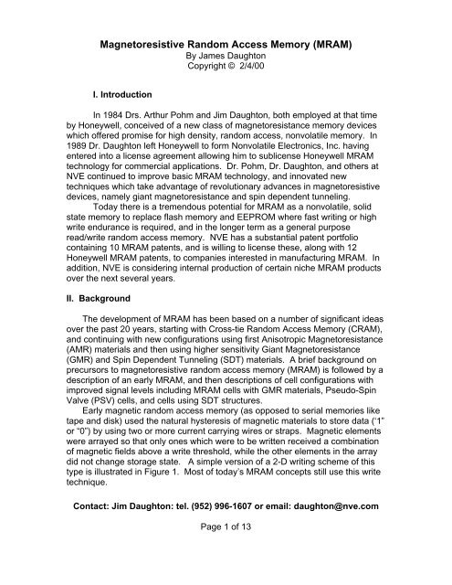
Magnetoresistive Random Access Memory (MRAM) Technology (.pdf)
Magnetoresistive Random Access Memory (MRAM) Technology (.pdf)
Magnetoresistive Random Access Memory (MRAM) Technology (.pdf)

Create successful ePaper yourself
Turn your PDF publications into a flip-book with our unique Google optimized e-Paper software.
<strong>Magnetoresistive</strong> <strong>Random</strong> <strong>Access</strong> <strong>Memory</strong> (<strong>MRAM</strong>)<br />
By James Daughton<br />
Copyright © 2/4/00<br />
I. Introduction<br />
In 1984 Drs. Arthur Pohm and Jim Daughton, both employed at that time<br />
by Honeywell, conceived of a new class of magnetoresistance memory devices<br />
which offered promise for high density, random access, nonvolatile memory. In<br />
1989 Dr. Daughton left Honeywell to form Nonvolatile Electronics, Inc. having<br />
entered into a license agreement allowing him to sublicense Honeywell <strong>MRAM</strong><br />
technology for commercial applications. Dr. Pohm, Dr. Daughton, and others at<br />
NVE continued to improve basic <strong>MRAM</strong> technology, and innovated new<br />
techniques which take advantage of revolutionary advances in magnetoresistive<br />
devices, namely giant magnetoresistance and spin dependent tunneling.<br />
Today there is a tremendous potential for <strong>MRAM</strong> as a nonvolatile, solid<br />
state memory to replace flash memory and EEPROM where fast writing or high<br />
write endurance is required, and in the longer term as a general purpose<br />
read/write random access memory. NVE has a substantial patent portfolio<br />
containing 10 <strong>MRAM</strong> patents, and is willing to license these, along with 12<br />
Honeywell <strong>MRAM</strong> patents, to companies interested in manufacturing <strong>MRAM</strong>. In<br />
addition, NVE is considering internal production of certain niche <strong>MRAM</strong> products<br />
over the next several years.<br />
II. Background<br />
The development of <strong>MRAM</strong> has been based on a number of significant ideas<br />
over the past 20 years, starting with Cross-tie <strong>Random</strong> <strong>Access</strong> <strong>Memory</strong> (CRAM),<br />
and continuing with new configurations using first Anisotropic Magnetoresistance<br />
(AMR) materials and then using higher sensitivity Giant Magnetoresistance<br />
(GMR) and Spin Dependent Tunneling (SDT) materials. A brief background on<br />
precursors to magnetoresistive random access memory (<strong>MRAM</strong>) is followed by a<br />
description of an early <strong>MRAM</strong>, and then descriptions of cell configurations with<br />
improved signal levels including <strong>MRAM</strong> cells with GMR materials, Pseudo-Spin<br />
Valve (PSV) cells, and cells using SDT structures.<br />
Early magnetic random access memory (as opposed to serial memories like<br />
tape and disk) used the natural hysteresis of magnetic materials to store data (‘1”<br />
or “0”) by using two or more current carrying wires or straps. Magnetic elements<br />
were arrayed so that only ones which were to be written received a combination<br />
of magnetic fields above a write threshold, while the other elements in the array<br />
did not change storage state. A simple version of a 2-D writing scheme of this<br />
type is illustrated in Figure 1. Most of today’s <strong>MRAM</strong> concepts still use this write<br />
technique.<br />
Contact: Jim Daughton: tel. (952) 996-1607 or email: daughton@nve.com<br />
Page 1 of 13
<strong>Magnetoresistive</strong> <strong>Random</strong> <strong>Access</strong> <strong>Memory</strong> (<strong>MRAM</strong>)<br />
By James Daughton<br />
Copyright © 2/4/00<br />
Iy<br />
Operate Points<br />
Iy<br />
Ix<br />
Selected Cell<br />
No Switch<br />
• Ix, Iy Alone Doesn’t Switch Cell<br />
• Ix, Iy Together Switch Cell<br />
Figure 1. 2-D Magnetic <strong>Memory</strong> Cell Array And Selection Of Cell.<br />
These early memories (mostly magnetic core memories) used inductive<br />
signals for determining the storage state (“1” or “0”). A magnetic field (current)<br />
was used to “interrogate” the memory element, and the polarity of induced<br />
voltages in a sensing circuit depended on whether a “1” or “0” was stored.<br />
The first to propose a magneto-resistive readout scheme was Jack Raffel [1].<br />
His scheme stored data in a magnetic body, which in turn produced a stray<br />
magnetic field that could be detected by a separate magnetoresistive sensing<br />
element. The concept was not high density because it was difficult to get a<br />
sufficiently large external stray field from a small magnetic storage cell. This<br />
scheme of separating the magnetic storage element from the sensor has<br />
similarity with the schemes recently proposed for magnetized bodies sensed by<br />
Hall effect sensors [2].<br />
The first technology which used a magnetic element for storage and also<br />
used the same element for magnetoresistance readout was the Cross-tie<br />
Ix<br />
Contact: Jim Daughton: tel. (952) 996-1607 or email: daughton@nve.com<br />
Page 2 of 13
<strong>Magnetoresistive</strong> <strong>Random</strong> <strong>Access</strong> <strong>Memory</strong> (<strong>MRAM</strong>)<br />
By James Daughton<br />
Copyright © 2/4/00<br />
Block Point - “0”<br />
No Block Point - “1”<br />
US Patent 5197025, L. Schwee and P. Hunter, “Crosstie <strong>Random</strong><br />
<strong>Access</strong> <strong>Memory</strong> and a Process for the Fabrication Thereof” 1993<br />
Figure 2. Crosstie <strong>Random</strong> <strong>Access</strong> <strong>Memory</strong> (CRAM)<br />
Cell.<strong>Random</strong> <strong>Access</strong> <strong>Memory</strong> (CRAM) [3]. This cell used a slight difference<br />
in resistance of the cell depending on the presence or absence of a Block point<br />
to indicate a “1” or “0” as shown in Figure 2. There were difficulties in getting the<br />
cell to write consistently, and the difference in resistance between a “1” and “0”<br />
.was only about 0.1% of the inherent cell resistance, an impractically low signal.<br />
The first published proposal for fabricating magnetic memory cells on a<br />
silicon support chip used inductive read-out rather than magnetoresistive readout<br />
[4]. This was (and still is) an important concept for <strong>MRAM</strong> because<br />
interconnections between an array of magnetic cells and the required circuitry to<br />
make a memory are probably too complex for separate memory and support<br />
circuitry.<br />
III. <strong>Magnetoresistive</strong> <strong>Random</strong> <strong>Access</strong> <strong>Memory</strong> (<strong>MRAM</strong>)<br />
In the mid 1980’s an <strong>MRAM</strong> concept was developed at Honeywell which<br />
has some common features with most modern versions.<br />
• Writing using magnetic hysteresis<br />
• Reading using magnetoresistance of the same body where data is<br />
stored<br />
• <strong>Memory</strong> cells integrated on an integrated circuit chip<br />
Figure 3 illustrates the method of data storage in the <strong>MRAM</strong> cell. The cell<br />
consisted of two ferromagnetic films sandwiching a poor conductor (TaN), with<br />
the composite film etched into stripes as shown. A current through the stripe<br />
Contact: Jim Daughton: tel. (952) 996-1607 or email: daughton@nve.com<br />
Page 3 of 13
<strong>Magnetoresistive</strong> <strong>Random</strong> <strong>Access</strong> <strong>Memory</strong> (<strong>MRAM</strong>)<br />
By James Daughton<br />
Copyright © 2/4/00<br />
magnetized the NiFe clockwise or counterclockwise when aided by a current<br />
(field) from an orthogonal stripline. Current in either strip by itself would not<br />
change the storage state. Thus, a single memory cell could be selectively written<br />
in a 2D array [5].<br />
Figure 3. Earliest <strong>MRAM</strong> Concept.<br />
Reading of this cell depended on the differential resistance of the cell<br />
when a sense current was passed through it. Because the sense current creates<br />
a magnetic field which opposes the magnetization in one storage state, but is in<br />
the same direction in the other state, the angle of rotation was different for a “1”<br />
or “0”. The magnetic material used was a cobalt-permalloy alloy with a normal<br />
anisotropic magnetoresistance (AMR) ratio of about 2%. Despite improvements<br />
in reading methods [6], the maximum differential resistance of the cell between a<br />
“1” and a “0” when it was read was about ¼ of the 2% magnetoresistance, or<br />
about 0.5%. In real arrays with practical sense currents, this gave differential<br />
sense signals of 0.5 to 1.0 mV. These sense signals allowed 16K bit integrated<br />
<strong>MRAM</strong> chips to operate with a read access time of about 250 ns [7]. Write times<br />
for the <strong>MRAM</strong> was 100 ns, and could have been faster if needed. A<br />
photomicrograph of a 256K bit <strong>MRAM</strong> chip produced by Honeywell is shown in<br />
Figure 4.<br />
Contact: Jim Daughton: tel. (952) 996-1607 or email: daughton@nve.com<br />
Page 4 of 13
<strong>Magnetoresistive</strong> <strong>Random</strong> <strong>Access</strong> <strong>Memory</strong> (<strong>MRAM</strong>)<br />
By James Daughton<br />
Copyright © 2/4/00<br />
Figure 4. 256 K <strong>MRAM</strong> Chip (Courtesy of Honeywell).<br />
The discovery of Giant Magnetoresistance (GMR) materials in 1989 [8,9]<br />
gave hope for higher signals and faster read access time. In 1991 magnetic films<br />
sandwiching a copper layer and etched into stripes showed a magnetoresistance<br />
ratio of about 6%. This magnetic configuration fit the aforementioned <strong>MRAM</strong> cell<br />
with little modification. Since the read access times tends to improve as the<br />
square of the signal, normal scaling would indicate that the improvement of a<br />
factor of 3 in magnetoresistance would lead to a 9 times improvement in read<br />
access time. Read access times of under 50 ns were achieved for <strong>MRAM</strong> with<br />
GMR materials [10].<br />
Even with GMR materials this cell had serious limitations. The<br />
competition – semiconductor memory – was still faster because of the low <strong>MRAM</strong><br />
sense signal. Worse, there was a limit to the reduction of cell size because the<br />
cell would not work with sense lines narrower than about 1 micron. This was due<br />
to magnetization curling from the edges of the stripe, where the magnization is<br />
pinned along the stripe. Due to exchange, there are limits to how quickly the<br />
magnetization can change directions with distance, and near the center of a 1<br />
micron stripe, the magnetizations of the two magnetic layers in the sandwich<br />
would be directed substantially along the stripe, thus storing data very marginally.<br />
IV. Pseudo-Spin Valve (PSV)<br />
The invention of the Pseudo-Spin Valve (PSV) cell [11] significantly improved<br />
signal levels, thus improving the read access time of <strong>MRAM</strong> while maintaining<br />
Contact: Jim Daughton: tel. (952) 996-1607 or email: daughton@nve.com<br />
Page 5 of 13
<strong>Magnetoresistive</strong> <strong>Random</strong> <strong>Access</strong> <strong>Memory</strong> (<strong>MRAM</strong>)<br />
By James Daughton<br />
Copyright © 2/4/00<br />
densities competitive with other solid state memory technologies. Not only was<br />
nearly all of the (approximately) 6% GMR available, but also the signal swing<br />
was plus or minus 6%, making the difference between a “0” and “1” about 12% of<br />
the cell resistance. This gave an 8 times improvement over the original mode of<br />
operation, and put <strong>MRAM</strong> on a much more even footing with semiconductor<br />
memory for read access time.<br />
Figure 5. Pseudo-Spin Valve Cell.<br />
Figure 5 illustrates the construction of a PSV cell. There are two magnetic<br />
layers that have mismatched properties so that one tends to switch at lower fields<br />
than the other. This can be done by using two magnetic films of the same<br />
material, but with different thicknesses. In that case, the thinner film switches at<br />
lower fields, or is the “soft” film and the thicker film switches at a higher field, and<br />
is the “hard” film. The resistance is lowest at the fields where the hard film<br />
switches to align with the soft film. The soft film acts as a means of reading the<br />
storage state, which is stored in the hard film. Without switching the hard film,<br />
the soft film can be manipulated to be parallel or antiparallel to the hard film. As<br />
shown in Figure 6, with a sequence of word fields which starts with a negative<br />
field and ends with a positive field, the resistance either rises or falls, depending<br />
on whether a “1” or a “0” is stored. With simple electronics, the difference<br />
between the initial and final resistances can be sensed, and the polarity of this<br />
difference indicates whether a “1” or “0” is stored.<br />
PSV memory cells can be as narrow as 0.2 microns [12], and perhaps<br />
narrower, and using a 2D memory organization, PSV memory is probably the<br />
densest of the proposed <strong>MRAM</strong> schemes. The reported fields (currents) required<br />
to switch the hard layer have been too high to date for high density integrated<br />
circuits. PSV memory may find initial applications as a replacement for EEPROM<br />
or flash memory when high density or fast writing is important.<br />
Contact: Jim Daughton: tel. (952) 996-1607 or email: daughton@nve.com<br />
Page 6 of 13
<strong>Magnetoresistive</strong> <strong>Random</strong> <strong>Access</strong> <strong>Memory</strong> (<strong>MRAM</strong>)<br />
By James Daughton<br />
Copyright © 2/4/00<br />
% of maximum GMR<br />
1<br />
0.9<br />
0.8<br />
0.7<br />
0.6<br />
0.5<br />
0.4<br />
0.3<br />
0.2<br />
0.1<br />
0<br />
-150 -100 -50 0 50 100 150<br />
Field (Oe)<br />
Figure 6. Pseudo-Spin Valve Resistance vs Magnetic Field Characteristic.<br />
V. Spin Dependent Tunneling (SDT) <strong>Memory</strong><br />
Spin Dependent Tunneling (SDT) devices provides higher percentage<br />
magnetoresistance than sandwich or PSV structures, and thus has the potential<br />
for higher signals and higher speed. Recent results indicate SDT tunneling<br />
giving over 40% magnetoresistance [13,14] compared to 6-9 %<br />
magnetoresistance in good PSV cells.<br />
(3X3 Xistor/Cell Array)<br />
N.C.<br />
N.C.<br />
Sense<br />
Electronics<br />
ON<br />
N.C.<br />
N.C.<br />
ON<br />
Contact: Jim Daughton: tel. (952) 996-1607 or email: daughton@nve.com<br />
Page 7 of 13<br />
Pass<br />
Transistors<br />
<strong>Memory</strong><br />
Array<br />
Figure 7. 3x3 Array of SDT <strong>Memory</strong> Cells.
<strong>Magnetoresistive</strong> <strong>Random</strong> <strong>Access</strong> <strong>Memory</strong> (<strong>MRAM</strong>)<br />
By James Daughton<br />
Copyright © 2/4/00<br />
The physical and magnetic similarities between magnetic sandwiches with<br />
copper interlayers and SDT magnetic sandwiches with dielectric interlayers<br />
suggests that SDT memory cells can be constructed in much the same fashion<br />
as PSV cells [15]. This is true with some limitations. The resistance of small<br />
tunneling cells tend to be at least several 1000’s of Ohms, and they are subject<br />
to dielectric breakdown at the 1V to 2V level. Thus, currents of more than about<br />
1 mA through the devices is not practical, and the currents used to sense the<br />
state of the SDT cell probably cannot be used to aid in the switching of the cell,<br />
unlike PSV cells. This suggests extra contacts and lower density for the SDT<br />
than for the PSV cell. Although there are also some time constant limitations for<br />
PSV cells, recent data [13] on lower resistance indicates that this problem can be<br />
overcome. The intrinsic speed of SDT elements configured into a DRAM type<br />
architecture (see Figure 7) or a flip-flop like cell (see Figure 8) should provide<br />
signals of 30-40 mV, which is comparable to semiconductor memory cells signal<br />
levels, and should thus run at comparable speeds. SDT memory show promise<br />
for high performance nonvolatile applications, including embedded latches for<br />
reconfigurable computing.<br />
Supply<br />
Low<br />
High<br />
N.C.<br />
Figure 8. SDT Static RAM Cell<br />
VI. Current Status<br />
Several large companies currently have R&D programs on <strong>MRAM</strong><br />
technology, and Honeywell has announced working <strong>MRAM</strong> components. With<br />
numerous competitors in the field, there has been a reluctance to publish results.<br />
But it is clear that <strong>MRAM</strong> has the potential to be as fast and dense as DRAM with<br />
the additional advantage of nonvolatility. Compared with flash and EEPROMs,<br />
<strong>MRAM</strong> writes much faster and does not deteriorate with millions of write cycles.<br />
Contact: Jim Daughton: tel. (952) 996-1607 or email: daughton@nve.com<br />
Page 8 of 13
<strong>Magnetoresistive</strong> <strong>Random</strong> <strong>Access</strong> <strong>Memory</strong> (<strong>MRAM</strong>)<br />
By James Daughton<br />
Copyright © 2/4/00<br />
Ferroelectric RAM (FRAM) is like <strong>MRAM</strong> in that it is nonvolatile and fast write,<br />
and there has been some limited commercial applications. While FRAM is a<br />
competitor to <strong>MRAM</strong>, it is likely that <strong>MRAM</strong> can be denser, and thus less<br />
expensive.<br />
VII. Challenges<br />
Present day challenges for <strong>MRAM</strong> technology include 1) reducing drive<br />
currents, 2) eliminating cell instabilities due to magnetization vortices, 3)<br />
improving modes of operation at nanometer dimensions to avoid fundamental<br />
thermal instabilities, and 4) finding applications with sufficient volumes and<br />
performance advantages to make <strong>MRAM</strong> manufacturing costs competitive.<br />
To be practical, dense <strong>MRAM</strong> cells should operate with less than a few mA<br />
currents when the lithography is at the 0.2 – 0.3 micron dimensions. Two<br />
reasons are: to stay within the current carrying capability of thin, narrow metal<br />
lines, and to be compatible with the center-to-center circuit spacing at the edge<br />
of the magnetic array. Reported data shows more than 10 times the desired<br />
current densities. Several mitigating ideas have emerged. One is to coat or<br />
“keeper” the tops and edges of the strip lines used in the memory array as shown<br />
in Figure 9. This has been shown to reduce word currents by a factor of 3 in<br />
unpublished work at NVE (see Figure 10]. An additional idea is to reduce the<br />
rise time of pulses, which takes advantage of the gyro-magnetic nature of the<br />
magnetization. This technique has reduced the required drive currents by a<br />
factor of more than 2 as shown in Figure 11 [16]. Devising methods whereby<br />
required current levels scale down with size of the memory cell will continue to be<br />
a challenge for <strong>MRAM</strong>.<br />
Figure 9. Cross-Section of “Keepered” Word Line (intermediate process step)<br />
Contact: Jim Daughton: tel. (952) 996-1607 or email: daughton@nve.com<br />
Page 9 of 13
<strong>Magnetoresistive</strong> <strong>Random</strong> <strong>Access</strong> <strong>Memory</strong> (<strong>MRAM</strong>)<br />
By James Daughton<br />
Copyright © 2/4/00<br />
In the 1980’s it was believed that as the memory cells approached the<br />
dimensions of a domain wall width, there would be no more problems with multidomain<br />
magnetization in the cells, i.e. the magnetization would act as a single<br />
collection of spins with only one rest state. This myth was shown to be false by<br />
both experiment and data. Anomolies called “vortices” can occur in cells as<br />
small as a few tenths of a micron in diameter [17], and example of which is<br />
illustrated in a simulation shown in Figure 12. These can be prevented in PSV<br />
cells by using sharp ends [16], one example of which is shown in Figure 13, but<br />
at the expense of cell area. Recently, a circumferential magnetization storage<br />
mode in round <strong>MRAM</strong> cells has been proposed [18]. Vortices are the<br />
unanticipated problem in <strong>MRAM</strong> technology.<br />
Figure 10. Field Enhancement Due To Keepers.<br />
Contact: Jim Daughton: tel. (952) 996-1607 or email: daughton@nve.com<br />
Page 10 of 13
<strong>Magnetoresistive</strong> <strong>Random</strong> <strong>Access</strong> <strong>Memory</strong> (<strong>MRAM</strong>)<br />
By James Daughton<br />
Copyright © 2/4/00<br />
Figure 11. Word Field Required For Switching vs Rise Time.<br />
Figure 12. Simulated Spin Valve <strong>Memory</strong> Cell Anomaly.<br />
Contact: Jim Daughton: tel. (952) 996-1607 or email: daughton@nve.com<br />
Page 11 of 13
<strong>Magnetoresistive</strong> <strong>Random</strong> <strong>Access</strong> <strong>Memory</strong> (<strong>MRAM</strong>)<br />
By James Daughton<br />
Copyright © 2/4/00<br />
Everitt et al, “Pseudo Spin Valve <strong>MRAM</strong> Cells with Sub-<br />
Micron Critical Dimensions”, IEEE Trans. Magn. 1998<br />
Figure 13. Sharp Bit Ends For Improving PSV Stability.<br />
The stability of the <strong>MRAM</strong> cell can be looked at as an energy well problem,<br />
where the energy associated with storage is MHcV, where Hc is a critical field<br />
which prevents magnetization reversal, M is the saturation magnetization, and V<br />
is the volume of the magnetic material in the cell. As the volume is reduced, the<br />
ratio approaches some multiple of kT (about 20) at which the error rate in the<br />
memory becomes unacceptable. Making Hc ever higher does not work because<br />
of the current required to write and the resultant heating of the cell (raising kT).<br />
With the present modes of operating, the practical lower limit to <strong>MRAM</strong> storage<br />
area would be about 0.1 micron on a side. A new idea is to use heat to help<br />
select the cell for writing and use the Curie point of an antiferromagnet to enable<br />
writing with a low current. Then at cooler temperatures, the energy well can be<br />
very deep. This is an idea that NVE is working on actively.<br />
The last challenge is getting <strong>MRAM</strong> into high production levels. It requires<br />
investment, and a lot of it, perhaps as much as a billion dollars. It will take<br />
commitment from one or more companies to manufacture <strong>MRAM</strong> in high volume,<br />
in order to realize the tremendous potential of <strong>MRAM</strong> as a mainstream<br />
nonvolatile memory technology, but with the right investment, <strong>MRAM</strong> can be a<br />
very important mainstream memory technology.<br />
References<br />
1) J. Raffel and T. Crowder, IEEE Trans. Electronic Components 13, No. 5, p. 611 (1964)<br />
2) M. Naiman, Intermag 1965, Paper 11-2.<br />
3) M. Johnson, B. Bennett, and M. Yang, “Hybrid Ferromagnetic Semiconductor Nonvolatile<br />
<strong>Memory</strong>”, IEEE Trans. Magn. 34, No. 4, pp 1054-1059 (1998).<br />
4) L. Schwee, P. Hunter, K. Restorff, and M. Shepard, “The Concept And Initial Studies Of A<br />
Crosstie <strong>Random</strong> <strong>Access</strong> <strong>Memory</strong>”, J. Appl. Phys. 53, No. 3, pp.2762-2764 (1982).<br />
5) IBM Disclosure Bulletin<br />
Contact: Jim Daughton: tel. (952) 996-1607 or email: daughton@nve.com<br />
Page 12 of 13
<strong>Magnetoresistive</strong> <strong>Random</strong> <strong>Access</strong> <strong>Memory</strong> (<strong>MRAM</strong>)<br />
By James Daughton<br />
Copyright © 2/4/00<br />
6) J. Daughton, "<strong>Magnetoresistive</strong> <strong>Memory</strong> <strong>Technology</strong>", Thin Solid Films, 216 pp 162-168<br />
(1992).<br />
7) A. Pohm, C. Comstock, and A. Hurst, “Quadrupled Non-Distructive Outputs From <strong>Memory</strong><br />
Cells Using Reversed Word Fields”, J. Appl. Phys. 67, pp. 4881-83 (1990).<br />
8) A. Hurst and G. Granley, “Projected Applications, Status, and Plans For Honeywell High<br />
Density, High Performance Nonvolatile <strong>Memory</strong>”, Proceedings of the 1996 Nonvolatile<br />
<strong>Memory</strong> <strong>Technology</strong> Conference, Albuquerque, NM, 1996.<br />
8) M. Baibich, J. Broto, A. Fert, F. Nguyen Van Dau, F. Petroff, P. Eitenne, G. Creuzet, A.<br />
Friederich, and J. Chazelas, "Giant Magnetoresistance of (001) Fe/(001) Cr Magnetic<br />
Superlattices", Physical Review Letters, Vol. 61, no. 21, p.2472 (1990).<br />
9) J. Barnas, A. Fuss, R. Camley, P. Grunberg, and W. Zinn, "Novel Magnetoresistance Effect<br />
in Layered Magnetic Structures: Theory and Experiment", Physical Review B, Vol. 42, no. 13,<br />
p. 8110 (1990).<br />
10) G. Panning, D. Erstad, W. Heikkila, A. Hurst, and H. Kaakani, “Honeywell <strong>Technology</strong> And<br />
Product Overview And Plans”, 1999 GOMAC Conference, March 8-11, 1999, Monterey, CA.<br />
11) A. Pohm, B. Everitt, R. Beech, and J. Daughton, “Bias Field And End Effects On The<br />
Switching Thresholds of ‘Pseudo Spin Valve’ <strong>Memory</strong> Cells”, IEEE Trans. Magn. 33, pp<br />
3280-3282 (1997).<br />
12) B. Everitt, A. Pohm, R. Beech, A. Fink, and J. Daughton, “Pseudo Spin Valve <strong>MRAM</strong> Cells<br />
With Sub-Micrometer Critical Dimensions”, IEEE Trans. Magn. 34, No. 4, pp.1060-1062<br />
(1998).<br />
13) S. Parkin, “Magnetic Tunneling Junction Devices For Non-Volatile <strong>Random</strong> <strong>Access</strong> <strong>Memory</strong>”,<br />
Paper GA-01 Presented At 1999 Intermag Conference in Kyongiu, Korea May 18-21, 1999.<br />
14) S. Carsoso, V. Gehanno, R. Fereira, and P. Freitas, “Ion Beam Deposition And Oxidation Of<br />
Spin Dependent Tunnel Junctions”, Paper FC-03 Presented At 1999 Intermag Conference in<br />
Kyongiu, Korea May 18-21, 1999.<br />
15) J.M. Daughton, “Magnetic Tunneling Applied To <strong>Memory</strong>”, J. Appl. Phys. 81, No. 8, pp 3758-<br />
63, (1997).<br />
16) A. Pohm, J. Anderson, R. Beech, and J. Daughton, “Effect Of Write Field Rise Times On The<br />
Switching Thresholds Of Pseudo Spin Valve <strong>Memory</strong> Cells”, J. Appl. Phys. 85, No. 8, pp<br />
4771-4772 (1999).<br />
17) J. Gadbois and J.-G. Zhu, “The Effect Of End And Edge Shape On The Performance of<br />
Pseudo-Spin Valve Memories”, IEEE Trans. Magn. 34, No. 4, pp. 1066-1068 (1998).<br />
18) K. Bussmann, G. Prinz, S.-F. Cheng, J.-G. Zhu, Y. Zheng, J. Daughton, R. Beech, D. Wang,<br />
and R. Womack, “Current Perpendicular-To-Plane GMR For <strong>Magnetoresistive</strong> RAM, Paper<br />
GA-03 Presented At 1999 Intermag Conference in Kyongiu, Korea May 18-21, 1999.<br />
Contact: Jim Daughton: tel. (952) 996-1607 or email: daughton@nve.com<br />
Page 13 of 13