John Hardy 990.pdf - Free Pro Audio Schematics
John Hardy 990.pdf - Free Pro Audio Schematics
John Hardy 990.pdf - Free Pro Audio Schematics

Create successful ePaper yourself
Turn your PDF publications into a flip-book with our unique Google optimized e-Paper software.
Mail:<br />
Ship:<br />
P.O. Box AA631<br />
Evanston, IL 60204 USA<br />
1728 Brummel St.<br />
Evanston, IL 60202 USA<br />
THE JOHN HARDY COMPANY<br />
990 Discrete Op-Amp<br />
Phone: 847-864-8060<br />
Toll <strong>Free</strong>: 866-379-1450<br />
Fax: 847-864-8076<br />
www.johnhardyco.com<br />
October 6, 2003<br />
The 990 discrete op-amp is the finest op-amp available for audio applications. If you want<br />
superior sound quality, the 990 can provide it. The 990 is used in the most critical audio<br />
applications. Leading recording studios, remote recording companies, disc and CD<br />
mastering facilities, TV and radio stations use the 990 for superior performance. Several mic<br />
preamps and other products using the 990 are available from the <strong>John</strong> <strong>Hardy</strong> Co.<br />
Features<br />
Circuit design of the 990 is by Deane<br />
Jensen of Jensen Transformers, who was<br />
awarded U.S. patent #4,287,479 for this<br />
design. Every aspect of the 990's design<br />
and performance was optimized through<br />
extensive computer aided design and<br />
analysis. Each component of this discrete<br />
op-amp was carefully chosen for its specific<br />
task, providing superior performance<br />
compared to monolithic op-amps and other<br />
discrete op-amps. For complete design<br />
theory, circuit details and specifications,<br />
please see the Jensen engineering report.<br />
Packaging and production design of the<br />
990 is by <strong>John</strong> <strong>Hardy</strong> of the <strong>John</strong> <strong>Hardy</strong><br />
Co. The design enables this 41-component<br />
circuit (44 components for the 990A<br />
and 47 components for the 990C) to be<br />
constructed on a circuit board 1” square,<br />
with final module dimensions after encapsulation<br />
of 1.125” square by 0.600” high.<br />
The dimensions and pinouts conform to<br />
the API-2520 package, allowing direct replacement<br />
in most applications.<br />
Discrete vs. monolithic op-amps. An opamp<br />
typically consists of dozens of diverse<br />
components including transistors,<br />
diodes, resistors, capacitors and occasionally,<br />
inductors. The fundamental difference<br />
between a discrete op-amp and a<br />
monolithic op-amp is the way these diverse<br />
components are brought together to<br />
make a working op-amp.<br />
A discrete op-amp is made from individual<br />
(discrete) transistors, diodes, resistors, capacitors,<br />
and occasionally, inductors that<br />
are brought together on a circuit board or<br />
other substrate to create the final circuit.<br />
Each diverse component is fabricated on a<br />
manufacturing line that is fully optimized<br />
for that specific part. Therefore, each<br />
component is the very best it can be. Lownoise<br />
input transistors are fully optimized<br />
for their unique requirements, high-power<br />
output transistors are fully optimized for<br />
their unique and very different requirements.<br />
Precision resistors come from<br />
manufacturing lines that are dedicated to<br />
making precision resistors. Capacitors<br />
come from optimized capacitor lines.<br />
Only after these fully optimized components<br />
are fabricated are they brought together<br />
on a circuit board or substrate.<br />
A monolithic op-amp starts with a single<br />
chip (monolith) of silicon that is typically<br />
1/16” square. This chip is the substrate<br />
upon which the dozens of diverse components<br />
are created. Note that all components<br />
are created on the same chip, and<br />
you simply cannot have the world's best<br />
input transistors, and the world's best output<br />
transistors, and precision resistors and<br />
capacitors on the same tiny chip. There<br />
are unavoidable compromises due to limitations<br />
in the fabrication process. If the<br />
process is optimized for low-noise input<br />
transistors there will likely be a compromise<br />
in the high-power output transistors,<br />
etc. It is impossible to incorporate the two<br />
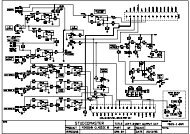
inductors used in the 990 (L1 and L2 on<br />
1<br />
the 990 schematic, page 3) into a monolithic<br />
design. Each of them is 0.235”D x<br />
0.400”H. How do you work that into the<br />
1/16” square chip of silicon of a typical<br />
monolithic op-amp? You don't!<br />
Even the small size of the typical silicon<br />
chip is a limiting factor. To fit all of the<br />
parts on such a small chip they must be<br />
made much smaller than might otherwise<br />
be desired. The reduced size causes a reduced<br />
ability to dissipate heat. The closer<br />
spacing of components and circuit traces<br />
reduces the maximum voltage levels that<br />
the circuit can tolerate.<br />
Monolithic op-amps are marvels of technology,<br />
but when performance is critical,<br />
they cannot match a discrete op-amp. A<br />
discrete op-amp costs more and is larger<br />
than a monolithic op-amp, but it offers superior<br />
performance in many ways:<br />
Lower noise. The 990 is an extremely quiet<br />
op-amp, particularly with low<br />
impedance sources. This can provide as<br />
much as 8dB of improvement in signal-tonoise<br />
ratios in summing amp applications,<br />
compared to the popular 5534 monolithic<br />
op-amp.<br />
The 990 also provides extremely low<br />
noise when used in mic preamp applications.<br />
The <strong>John</strong> <strong>Hardy</strong> Company manufactures<br />
the M-1 Mic Preamp, the M-2<br />
Mic Preamp, the Jensen Twin Servo ® 990<br />
Mic Preamp and several mic preamp<br />
cards using the 990 discrete op-amp.<br />
Please refer to the data packages for those<br />
products. The application notes later in<br />
this package include a schematic of the<br />
mic preamp circuitry of the M-1 and a<br />
discussion of circuit details.
One of the reasons the 990 is so quiet is<br />
its use of the National Semiconductor<br />
LM-394 supermatched transistor pair for<br />
the input pair of transistors (Q1 and Q2<br />
on the 990 schematic). Since the input<br />
pair of transistors in any op-amp should<br />
be as closely matched in performance as<br />
possible, the LM-394 is ideal because<br />
both transistors of the LM-394 are fabricated<br />
on the same chip of silicon, thus<br />
avoiding differences that would exist between<br />
separate chips of silicon. This is a<br />
unique situation where the monolithic<br />
process is superior to discrete. The process<br />
requirements are identical for both<br />
transistors, so they should be made on the<br />
same monolithic substrate.<br />
But National goes much farther by fabricating<br />
100 transistors on the same chip instead<br />
of just two. 25 transistor pairs (50<br />
transistors) from across the chip are connected<br />
in parallel to form Q1, and the other<br />
25 pairs from across the chip are connected<br />
in parallel to form Q2. This causes<br />
even slight variations across the chip to be<br />
averaged out, typically reducing errors by<br />
an order of magnitude. Plus, having multiple<br />
transistors in parallel reduces noise.<br />
The silicon chip of the LM-394 is about<br />
1/16” square, the same size as the entire<br />
chip of a typical monolithic op-amp! No<br />
doubt National Semiconductor decided to<br />
make the finest possible supermatched<br />
transistor pair, using whatever size chip<br />
was required.<br />
High output power. The 990 provides<br />
much higher output power than monolithic<br />
op-amps. This is because the MJE-181<br />
and MJE-171 discrete output transistors<br />
(Q8 and Q9) are much larger than the<br />
ones found in monolithic op-amps (and<br />
some other discrete op-amps), so they can<br />
handle much more power. They were designed<br />
from the ground up as power transistors.<br />
They use a silicon chip that is as<br />
large as the chip in a typical monolithic<br />
op-amp. The chip is attached to a metal<br />
back-plate for improved heat-sinking and<br />
heat dissipation. Each transistor is about<br />
as large as an 8-pin DIP op-amp.<br />
Then the 990 package comes into play.<br />
The metal back-plates of the MJE-181<br />
and MJE-171 transistors are bonded to<br />
the aluminum shell of the 990 using a<br />
high thermal conductivity epoxy. This<br />
provides exceptional heat-sinking of the<br />
transistors. The 990 package has about 14<br />
times the surface area of a typical 8-pin<br />
DIP op-amp, greatly increasing its ability<br />
to dissipate heat. It is easy to see how the<br />
990 can handle much higher power levels<br />
than the typical monolithic op-amp. In<br />
fact, the 990 can drive 75Ω loads to full<br />
output level, while monolithic op-amps<br />
are limited to loads of 600Ω at best, and<br />
more typically 2kΩ. Some discrete opamps<br />
use much smaller output transistors<br />
than the MJE-181 and MJE-171. The<br />
transistors have smaller chips and are<br />
lacking a metal back plate critical for heat<br />
dissipation. They cannot handle as much<br />
power as the MJE-181 and MJE-171.<br />
The ability to drive lower-impedance<br />
loads is important for two reasons. First,<br />
the 990 can easily drive multiple power<br />
amps, or pots, or other devices, with less<br />
concern for cumulative loading. Second,<br />
the resistors, capacitors and other parts<br />
that are connected around the 990 to determine<br />
the function of the circuit<br />
(preamp, EQ, etc.) can be scaled down to<br />
much lower impedances than those of a<br />
monolithic design. This can result in lower<br />
noise. Some monolithic op-amps are<br />
theoretically capable of very low noise<br />
performance, but their inability to drive<br />
low impedances without increased distortion<br />
or decreased headroom results in<br />
compromised performance.<br />
Low noise and high output power. When<br />
you have the combination of low noise<br />
and high output power in the same opamp,<br />
you can often eliminate extra opamp<br />
stages in equipment. Going back to<br />
the M-1 mic preamp as an example, the<br />
990 provides the extremely low noise that<br />
is required in a mic preamp, and the high<br />
output power that is required in a line<br />
driver or main output stage. There is no<br />
need to have two stages – one for low<br />
noise and one for high output power.<br />
Your equipment is simpler with fewer<br />
stages. The signal path is shorter, resulting<br />
in less signal degradation. Discrete<br />
op-amps cost more than monolithics, but<br />
when you use fewer of them, the higher<br />
cost is less of a factor.<br />
Higher voltage ratings. The components of<br />
the 990 discrete op-amp are capable of<br />
handling higher voltages than those in<br />
most monolithic op-amps. This allows the<br />
990 to operate with ±24V power supplies,<br />
while the typical monolithic op-amp is<br />
limited to ±18V power supplies. It is very<br />
common for monolithic op-amps to be operated<br />
at ±15V, sometimes even ±12V. In<br />
audio terms, this means that the monolithic<br />
op-amps have reduced headroom. The<br />
990 with ±24V power supplies is capable<br />
of output levels of greater than +24dBu,<br />
while most monolithic op-amps clip at<br />
2<br />
least several dB below that due to the reduced<br />
power supply voltages.<br />
Precision passive parts. The 990 uses 1%<br />
100ppm metal film resistors and ultra-stable<br />
COG/NPO ceramic capacitors with<br />
much better specifications than the ones<br />
typically found in monolithic op-amps.<br />
See the special report about ceramic capacitors<br />
on page 8 for important information<br />
about this superior type of capacitor.<br />
It sounds better! Most important of all is<br />
the fact that the 990 sounds better than<br />
monolithic op-amps. The 990 does not<br />
suffer from the many compromises of the<br />
monolithic manufacturing process. Some<br />
people think that solid-state equipment is<br />
cold and harsh sounding. Not so with the<br />
990!<br />
Applications. The 990 offers the finest<br />
performance in summing amps, mic<br />
preamps, phono preamps, tape-head<br />
preamps, A/D and D/A converters, equalizers<br />
and line drivers. The sensitivity of<br />
measurement equipment can be increased<br />
by the low noise of the 990. Application<br />
notes follow.<br />
Models. The 990 is available in three circuit<br />
versions: the original 990, the 990A<br />
and the 990C. The original 990 has been<br />
available since 1979 and has established<br />
itself as the finest op-amp available for<br />
audio applications. The 990A adds three<br />
components to the original 990 circuit to<br />
provide protection in the rare event the<br />
positive power supply is lost while the opamp<br />
is driving an extremely low DC<br />
impedance such as the primary of an output<br />
transformer. Under those conditions<br />
the original 990 circuit would consume<br />
higher than normal current from the negative<br />
supply, but the “A” modification prevents<br />
the excess current flow. The 990C<br />
is a further development of the “A” version,<br />
allowing the op-amp to operate over<br />
a wide range of power supply voltages.<br />
Other additional components provide reduced<br />
offset voltage.<br />
Model# Application<br />
990-12V ±12V power supplies.<br />
990-15V ±15V power supplies.<br />
990-18V ±18V power supplies.<br />
990-24V ±24V power supplies.<br />
990A-12V ±12V power supplies.<br />
990A-15V ±15V power supplies.<br />
990A-18V ±18V power supplies.<br />
990A-24V ±24V power supplies.<br />
990C ±12 to ±24V power supplies.
Package details. The 990 is packaged in a<br />
black-anodized aluminum potting shell<br />
filled with a soft silicone material to encapsulate<br />
the components. The soft silicone<br />
eliminates physical stresses that<br />
could exist if the circuitry were encapsulated<br />
in a hard epoxy. Hard epoxies expand<br />
and contract at a higher rate than<br />
most electronic components as the temperature<br />
rises and falls. The hardness and<br />
higher expansion rate of the epoxy can<br />
cause stress fractures in some types of<br />
electronic parts. The soft silicone eliminates<br />
the problem.<br />
The metal back plates of the power transistors<br />
are bonded directly to the aluminum<br />
shell using an epoxy with high<br />
thermal conductivity, assuring maximum<br />
heat sinking of the transistors. The black<br />
anodized finish of the shell provides<br />
maximum thermal emission. The package<br />
measures 1.125” x 1.125” x 0.600”<br />
(LxWxH), not including the pin extension<br />
of 0.233”. The package is fully<br />
compatible with the API-2520 op-amp.<br />
Pins are 0.040”D, gold plated.<br />
Reliability. To ensure long-term reliability<br />
at temperature extremes, 1% 100ppm<br />
metal film resistors are used for R1<br />
through R12. The capacitors in the signal<br />
path are ultra-stable (±30ppm) monolithic<br />
ceramics, COG/NPO formulation.<br />
NOTE: Please see the special report on<br />
ceramic capacitors on page 8 for important<br />
information on this very special and<br />
superior formulation.<br />
All modules receive a total of 48 hours<br />
of active burn-in at 100°C (212°F).<br />
Component upgrades and other information.<br />
Many of the components listed in<br />
the Jensen engineering report have been<br />
upgraded in the 990s made by the <strong>John</strong><br />
<strong>Hardy</strong> Company to ensure long-term reliability<br />
at temperature extremes:<br />
R1 through R12 are upgraded from 5%<br />
carbon film resistors to 1% ±100ppm<br />
metal film resistors. Certain critical 1%<br />
resistors are individually trimmed to a<br />
higher degree of accuracy using proprietary<br />
trimming procedures.<br />
C1 through C3 are ultra-stable<br />
COG/NPO type ceramic capacitors. See<br />
the special report on ceramic capacitors<br />
on page 8. C4 and C5, which are not in<br />
the audio signal path, are upgraded from<br />
the Y5V type ceramic to the X7R ceramic,<br />
offering much greater stability over a<br />
wider temperature range.<br />
CR3 (1N914B diode) is replaced with a<br />
diode-connected PN4250A transistor as<br />
suggested in the Jensen engineering report.<br />
This provides better matching with<br />
Q3, also a PN4250A.<br />
The LM-394N is sometimes used in<br />
place of the LM-394H for Q1 and Q2. It<br />
provides identical performance to the<br />
LM-394H, and is packaged in the much<br />
easier to use 8-pin DIP package.<br />
Thermal coupling aids as listed in the<br />
Jensen engineering report are unnecessary.<br />
Components requiring thermal coupling<br />
are in direct contact with each other.<br />
High thermal conductivity epoxy is<br />
used in critical areas to complete the<br />
coupling process. The aluminum shell<br />
distributes heat evenly to all points.<br />
R15 and L3 (“output isolator”) are not<br />
part of the basic op-amp “triangle” and<br />
are not included in the 990. They are<br />
available separately and are recommended<br />
in many applications for best results.<br />
See the Jensen engineering report for details.<br />
990C Specifications (0dBu = 0.775V)<br />
Measurement<br />
Spec. Units<br />
Open-loop gain, DC to 30Hz 125 dB<br />
Gain error at 100dB gain<br />
0.4 dB<br />
Noise-voltage spectral density,<br />
each transistor<br />
0.8 nV/√Hz<br />
differential pair<br />
1.13 nV/√Hz<br />
Noise current spectral density<br />
1 pA/√Hz<br />
Noise index,<br />
1kW source resistance<br />
0.6 dB<br />
Equivalent input noise voltage,<br />
20kHz bandwidth, shorted input 160 nV<br />
Corresponding voltage level -133.7 dBu<br />
Maximum input voltage at unity gain 13.8 V<br />
Corresponding voltage level +25 dBu<br />
Input impedance, non-inverting input >10 M?<br />
Input bias current<br />
+2.2 μA<br />
Maximum output voltage,<br />
RL = 75W<br />
13.8 V<br />
Corresponding voltage level +25 dBu<br />
Maximum peak output current 260 mA<br />
Total harmonic distortion at 20kHz,<br />
VOUT = +24dBu<br />
RL = 75W, gain = 40dB 0.06 %<br />
RL = 75W, gain = 20dB 0.005 %<br />
RL = 600W, gain = 40dB 0.015 %<br />
Slew rate, RL = 150W<br />
18 V/µS<br />
Slew rate, RL = 75W<br />
16 V/µS<br />
Large-signal bandwidth,<br />
RL = 150W<br />
145 kHz<br />
Small-signal bandwidth,<br />
at unity gain (ft)<br />
10 MHz<br />
Gain-bandwidth product,<br />
10kHz to 100kHz<br />
>50 MHz<br />
Phase margin at 10MHz<br />
>38 deg<br />
Phase margin at 60 deg<br />
Response time at unity gain
Application Notes<br />
Following are several circuits for use with the 990 discrete op-amp. With<br />
proper attention to detail, you should achieve excellent results.<br />
Figure 1: Traditional mic preamp. Figure 1 shows a traditional transformerinput<br />
mic preamp, adjustable from 11.6 to 60dB of gain including the input<br />
transformer step-up of 5.6dB. The circuit has a bandwidth of 150kHz (-3dB).<br />
The Jensen JT-16-B mic-input transformer was designed specifically for the<br />
990.<br />
R1, R2 and C1 provide proper termination for the JT-16-B input transformer.<br />
R3, R4 and RV1 determine the AC voltage gain of the 990.<br />
C3 is used for two reasons. First, it keeps the input bias current (thus DC<br />
voltage) of the inverting input of the 990 from reaching the gain-adjust pot<br />
(RV1) where it could cause noise during adjustment of the pot. All op-amps<br />
have small amounts of bias current flowing at their inputs. Small DC<br />
voltages develop as these currents flow through whatever DC resistance path<br />
is available (E=IxR). Noise could occur during adjustment of the gain pot if<br />
more than about 1mV were to develop.<br />
C3 also keeps the DC gain of the 990 at unity so that a small difference<br />
between the DC voltages at the inverting and non-inverting inputs of the 990<br />
will not be amplified into a large offset voltage at the output.<br />
An optional offset compensation circuit is shown. The diode regulator and<br />
filter circuit supplies a current to the inverting input which compensates for<br />
the unequal DC resistances seen at the inputs. The offset voltage at each<br />
input is found by multiplying the input bias current (typically 2.2µA) by the<br />
DC resistance seen at that input. For the non-inverting input, the DC<br />
resistance is the input transformer secondary resistance in parallel with R1<br />
(6.19kΩ). For the inverting input R3 is the only DC path. Since the closed<br />
loop DC gain of the amplifier is unity, the DC offset at the output is equal to<br />
the difference of the offset voltages at the two inputs. The compensating<br />
current required into the inverting input is the offset voltage divided by R3<br />
(10kΩ). This compensation will significantly reduce the DC offset at the<br />
output for applications with no output coupling capacitor.<br />
C2 provides phase-lead compensation with a high-frequency cut-off of<br />
175kHz. C4 AC-couples the output of the 990 to remove any DC offset from<br />
the output.<br />
The use of capacitors C3 and C4 to control various DC problems is<br />
traditional. For a superior approach that eliminates these capacitors and the<br />
sonic problems they can cause, see the application note for the M-1 mic<br />
preamp on page 7.<br />
Figure 2: Phono preamp. Figure 2 shows a phono preamp with related<br />
component values and theoretical RIAA response figures. Gain is 41.7dB at<br />
1kHz. The circuit provides RIAA response accuracy of ±0.1dB. The values<br />
are taken from a paper by Lipshitz [1] which covers RIAA equalization<br />
networks and their proper design.<br />
Column 1 shows the exact calculated resistor and capacitor values. The<br />
nearest 1% resistor values are in column 2. Columns 3 and 4 show the values<br />
scaled by a factor of 10 to take advantage of the 990's lower noise figure at<br />
lower source impedances.<br />
C3 AC-couples the 990, causing DC gain to be unity. C3 could be eliminated<br />
if offset compensation were performed. See figure 1 for one method. See the<br />
M-1 mic preamp application note for superior methods. The ferrite beads at<br />
the input are optional to reduce RFI.<br />
REFERENCE: 1. Lipshitz, S., “On RIAA Equalization Networks”, Journal, <strong>Audio</strong><br />
Engineering Society, Vol. 27, #6, 6/79, pp. 458-481.<br />
Figure 3: Tape-head preamp. Figure 3 shows a tape-head preamp. Component<br />
values for 3.75 and 7.5 ips NAB equalization and a gain of 50dB at 1kHz are<br />
listed. Other gains and equalizations can be achieved using the formulas<br />
provided. Tape head specs and characteristics vary widely, so the values<br />
listed will probably require trimming. The results should be carefully<br />
examined.<br />
Tape heads with extremely low output levels will require additional gain. A<br />
2nd op-amp should be considered for that purpose. It should have flat<br />
response. Each op-amp should be set for equal gain at high frequencies<br />
(20kHz).<br />
This circuit is similar to the phono preamp, except it is tunable. The R2-C2<br />
network is at 300kHz performing phase-lead compensation rather than RIAA<br />
equalization. See Phono preamp for comments on C3 and ferrite beads.<br />
4
Figure 4: Two-stage mic preamp. Figure 4 shows a two-stage transformer-coupled<br />
mic preamp, recommended for situations where extremely high gain is required.<br />
The first stage is the same as the single-stage preamp of figure 1 except the<br />
maximum gain is about 40dB. A switchable second stage with 20dB of gain gives<br />
a choice of single-stage operation with up to 40dB of gain (including the<br />
transformer step-up), or two-stage operation with up to 60dB of gain. The 2nd<br />
stage could be changed to adjustable gain. Ideally each stage would have the same<br />
amount of gain.<br />
Offset voltage compensation can be performed on the first stage as described in<br />
the single-stage preamp text, or as shown in the M-1 application note. The second<br />
stage will have a low offset voltage because the inverting and non-inverting inputs<br />
see identical DC resistances (10kΩ). The techniques in the M-1 application note<br />
can be applied here too. See the data package for the Jensen Twin Servo ® 990 Mic<br />
Preamp, a superior two-stage mic preamp using the JT-16-B input transformer<br />
and 990C op-amp. It eliminates all coupling capacitors by using DC servo<br />
circuitry and input bias current compensation circuitry.<br />
Figure 5: Sockets. Many types of sockets for 0.040”D pins are available from<br />
several manufacturers. The <strong>John</strong> <strong>Hardy</strong> Co. uses and stocks the socket shown in<br />
figure 5, reprinted from the Concord catalog. The same part is also available from<br />
Cambion and Mill-Max. It can be soldered in place, or swaged (tool required).<br />
Here are three sources:<br />
CONCORD ELECTRONICS CORP. 212-777-6571<br />
30 Great Jones St. Part #09-9035-2-03<br />
New York, NY 10012<br />
CAMBION 617-491-5400<br />
445 Concord Ave. Part #450-3756-02-03<br />
Cambridge, MA 02238<br />
MILL-MAX 516-922-6000<br />
190 Pine Hollow Road, P.O. Box 300 Part #0344-2-19-15-34-27-10-0<br />
Oyster Bay, NY 11771<br />
Figure 6: Summing amp. Figure 6 show a summing amp with several optional<br />
features. Some applications require signals to be combined at unity gain, others<br />
require different gains. For example, the signal from channel 3 is attenuated by a<br />
potentiometer (typically 10dB of attenuation) before it enters the summing circuit.<br />
To restore the 10dB lost through the pot, a lower value is used for R IN , in this case<br />
3.16kΩ (see formulas). With many channels being summed, the output of the<br />
summing amp could become excessive. The final value for R IN is chosen based on<br />
the number of channels, signal levels, pot settings, etc.<br />
The non-inverting input may be grounded directly, or through a resistor. The<br />
value of the resistor should equal the DC source resistance seen by the inverting<br />
input, which is the parallel resistance of all the input resistors (assuming they are<br />
not AC-coupled) and the feedback resistor (R IN and R FB ). When both inputs of the<br />
990 see identical DC source resistances, the output offset voltage will be the<br />
lowest. This resistor can result in increased noise when compared to a grounded<br />
input. This problem can be overcome by adding a capacitor in parallel with this<br />
resistor. The capacitor has infinite impedance at DC, so the DC specs are<br />
unchanged. The impedance is much lower above DC, so the noise performance of<br />
the 990 is not significantly compromised. The value of the capacitor is not critical,<br />
with 0.1µF being a good starting point. If the non-inverting input is grounded a<br />
compensation current can be provided to the inverting input as shown in the M-1<br />
application note. This provides the lowest DC offset at the output of the 990, the<br />
lowest noise, and without the potential degradation caused by the capacitor.<br />
The actual terminating point for the non-inverting input is critical! In large<br />
consoles with many inputs, much noise can appear on the ground bus. Even a<br />
heavy ground bus will have a measurable resistance, with voltage appearing<br />
across the resistance. These voltages can be in the form of power supply noise,<br />
return currents (thus voltages) from other modules, etc. Although each input of the<br />
summing amp may be at unity gain, the overall gain of the summing amp is<br />
higher. The greater the number of inputs, the higher the overall gain will be. For<br />
example, 24 inputs with R IN of 10kΩ results in a final parallel resistance of 417Ω,<br />
for a voltage gain of 24 (27.6dB) (see the formulas). That is how much the ground<br />
bus noise would be amplified if the non-inverting input were terminated far from<br />
the signal sources being summed. The 990 is much quieter than most other opamps,<br />
but poor layout or grounding can defeat this advantage!<br />
Long summing busses cause increased stray capacitance at the inverting input,<br />
resulting in phase-shift of the feedback signal. In sufficient quantities, this can<br />
cause oscillation at ultra-high frequencies. Capacitance can be added in the<br />
feedback loop to compensate. An isolator (RL2) can be inserted between the<br />
summing bus and the inverting input. It maintains normal audio performance by<br />
providing less than 1Ω impedance throughout the audio bandwidth, while<br />
isolating stray capacitance by providing 39.2Ω impedance at ultra-high<br />
frequencies.<br />
5
M-1 Mic Preamp with Input Bias Current Compensation and DC Servo Circuitry<br />
Figure 7 shows the complete circuit of the<br />
MPC-1 mic preamp card used in the M-1<br />
and M-2 mic preamps, state-of-the-art mic<br />
preamps manufactured by the <strong>John</strong> <strong>Hardy</strong><br />
Co. This circuit eliminates all coupling<br />
capacitors traditionally used in mic preamp<br />
circuits, and the degradation in signal quality<br />
that they can cause. The main difference<br />
between the M-1 and the M-2 is the type of<br />
gain control: a 2-section potentiometer in the<br />
M-1, a 16-position rotary switch in the M-2.<br />
See the M-1 and M-2 data package for<br />
further details.<br />
At first glance capacitors seem like ideal<br />
components to use when trying to eliminate<br />
the DC voltages that always manage to creep<br />
into audio circuits. Capacitors have<br />
essentially infinite impedance at DC, and<br />
zero ohms impedance throughout the audio<br />
bandwidth if the value is large enough for<br />
the application.<br />
However, capacitors also have problems. See<br />
the special report about ceramic capacitors<br />
on page 8 for a discussion of one problem.<br />
Another problem is dielectric absorption.<br />
This is a condition where a small portion of<br />
the AC voltage that passes through the<br />
capacitor is temporarily absorbed by the<br />
dielectric of the capacitor, then released a<br />
short time later, causing a smearing of the<br />
sound. The severity of the problem depends<br />
on the type of dielectric in the capacitor, and<br />
other construction details.<br />
The problem tends to be unmeasurable with<br />
normal test methods, but can be audible.<br />
Some film dielectrics such as polypropylene,<br />
polycarbonate, polystyrene and Teflon<br />
minimize the problem. But when a circuit<br />
requires several hundred microfarads, it is<br />
out of the question to use them, both from a<br />
space and cost standpoint. A compromise<br />
approach has been to use electrolytic<br />
capacitors of the required large value, then<br />
add a 1.0µF or 0.1µF (or both) film capacitor<br />
in parallel, the theory being that low<br />
frequencies will be handled by the large<br />
electrolytic capacitor, and high frequencies<br />
(where the smearing would be most audible)<br />
will be handled by the small film capacitors.<br />
Traditional transformer-input mic preamps<br />
typically have two coupling capacitors in the<br />
signal path. Referring to the traditional mic<br />
preamp circuit of figure 1 they are C3 and<br />
C4. Their functions are discussed in that<br />
application note.<br />
Mic preamps with transformerless inputs<br />
have two additional coupling capacitors to<br />
keep the +48V phantom power supply<br />
voltage from reaching the active circuitry of<br />
the preamp where it would cause damage.<br />
An input transformer inherently blocks DC<br />
voltages, but does not suffer from the<br />
problem of dielectric absorption that<br />
capacitors have. Manufacturers of<br />
transformerless mic preamps might say that<br />
these capacitors cause less sonic damage<br />
than an input transformer. This is true of<br />
some input transformers, but not with the<br />
Jensen JT-16-B input transformer used in the<br />
M-1! This is Jensen's finest input<br />
transformer, and it is truly superior. See the<br />
M-1 data package for details.<br />
The M-1 takes a different approach. Rather<br />
than forcing the audio signal to pass through<br />
various capacitors to block the DC voltages<br />
(and, in the process, smear the audio signal),<br />
the DC voltages are nulled using special<br />
circuitry. The coupling capacitors are<br />
completely eliminated.<br />
The input bias current compensation circuit<br />
(“I BIAS”) on the MPC-1 mic preamp card<br />
provides an adjustable current to each input<br />
of the 990 op-amp. The current is the<br />
opposite polarity of the normal input bias<br />
currents of the 990 op-amp. When RV2 is<br />
properly adjusted, the input bias currents of<br />
the 990 are nulled so that no DC voltages are<br />
developed at the inputs of the 990.<br />
Traditionally a coupling capacitor (C3 in<br />
Figure 1) is used in series with the gain<br />
controls to keep DC voltages from reaching<br />
the gain controls where they could cause<br />
noise during adjustment of the control. The<br />
I BIAS circuit eliminates the need for this DCblocking<br />
capacitor.<br />
Since all input-related DC voltages have<br />
been nulled by the I BIAS circuit, it is no longer<br />
necessary to worry about a small difference<br />
in the voltages at the inputs being amplified<br />
into a large DC error or offset at the output<br />
of the 990. Therefore it is not necessary to<br />
limit the DC gain of the 990 to unity, a<br />
function that C3 also traditionally performs.<br />
Again, C3 can be eliminated by using the<br />
I BIAS circuitry.<br />
A +15V reference voltage is applied to the<br />
top of RV3, a 25-turn trim pot. The trimmed<br />
voltage is applied to the inputs of the 990 as<br />
a current through R9, R10, R11 and R12. C3<br />
and C4 act as noise filters.<br />
The DC servo (“SERVO”) circuit<br />
continuously monitors the output of the 990<br />
for the presence of any DC offset, and<br />
provides a correction to the inverting input<br />
of the 990 through R15. The final DC offset<br />
of the 990 is determined by the DC offset<br />
characteristics of the servo op-amp (U2).<br />
The AD705J was chosen because it has<br />
exceptional DC characteristics, with a<br />
typical DC offset of 200 microvolts and drift<br />
of 2 microvolts/°C. The DC offset<br />
performance of the AD705J is further<br />
improved by an order of magnitude through<br />
the use of trim pot RV3. (Currently the OP97<br />
is being used as the DC Servo op-amp).<br />
The servo circuit itself acts as an ultra-low<br />
frequency low-pass filter. The F -3dB<br />
frequency is so low (well below 1Hz) that<br />
essentially only DC is passed through the<br />
circuit and applied to the inverting input of<br />
the 990 as a nulling signal. The two R/C<br />
networks, R13/C5 and R14/C6, along with<br />
R15, determine the operating frequency. The<br />
capacitors have no detrimental effect on the<br />
audio signal because they only affect<br />
frequencies in the pass-band of the filter<br />
(well below 1Hz).<br />
Input Bias Current Calibration<br />
Whenever a 990 op-amp is replaced, it<br />
should be assumed that it has a different<br />
input bias current than the previous 990. The<br />
input bias current adjustment procedure<br />
should be performed as follows:<br />
1. Install the new 990, turn on the power and<br />
allow the unit to warm-up for at least 15<br />
minutes.<br />
2. Connect a DC voltmeter with at least 100<br />
microvolt sensitivity to the circuit as follows:<br />
The Positive lead connects to test point #1<br />
(“TP1”). This is the output of the 990 opamp.<br />
A long gold pin is provided for TP1,<br />
located along the left edge of the p.c. board<br />
near the rear. The negative lead connects to<br />
ground. A long gold pin is provided for this<br />
ground connection to the rear of the 990 opamp.<br />
3. Move JP3 to the ADJUST (“ADJ”)<br />
position. JP3 is located to the right of the<br />
990 op-amp. This disconnects the DC servo<br />
circuit so you can measure the DC offset of<br />
the 990 op-amp.<br />
4. Set the gain controls to minimum gain and<br />
make note of the DC offset measured at TP1.<br />
5. Set the gain controls to maximum gain<br />
and adjust RV2 so that the DC offset reading<br />
is within 1 millivolt of the reading taken<br />
when the gain controls were at minimum<br />
gain. It may take several seconds for this<br />
measurement to settle. RV2 is a 25-turn trim<br />
pot labeled I BIAS located to the right of the<br />
990 op-amp.<br />
6. Repeat steps 4 and 5 until the DC offset<br />
measurements are within 1 millivolt of each<br />
other at minimum and maximum gain. Note<br />
that both readings may be several millivolts,<br />
or even tens of millivolts. They might both<br />
be positive, or negative. The important thing<br />
is that they are within 1 millivolt of each<br />
other, and the same polarity.<br />
7. Move JP3 to the “RUN” position. This<br />
reconnects the DC servo. This should cause<br />
the DC offset voltage of the 990 op-amp to<br />
drop to well below 1 millivolt. In fact, the<br />
DC offset should drop to well below 100<br />
microvolts if the DC servo circuit is<br />
functioning properly.<br />
DC Offset Calibration<br />
The final DC offset of the MPC-1 mic<br />
preamp card is determined by the<br />
performance of the DC servo op-amp (U2).<br />
An AD705J or OP97 op-amp is used because<br />
it has excellent DC specifications. It is<br />
capable of providing a DC offset that is<br />
typically less than 200 microvolts without<br />
any additional trimming. This is excellent,<br />
but can be improved by an order of<br />
magnitude through the use of trim pot RV3.<br />
When making DC measurements below 100<br />
microvolts you will need a DC voltmeter<br />
with a sensitivity and resolution of at least 1<br />
microvolt. Most meters will have DC offsets<br />
of their own to deal with, as well as drift due<br />
to time and/or temperature. Even the cables<br />
and test probes can introduce errors. Follow<br />
the meter instructions very carefully<br />
regarding warm-up time and zeroing<br />
procedures.<br />
When you have properly warmed-up and<br />
zeroed your meter, adjust RV3 until the DC<br />
offset measurement between TP1 and ground<br />
is as close to ZERO microvolts as possible.<br />
7
Ceramic Capacitors<br />
Ceramic capacitors have a bad reputation in audio circles. It is only partially deserved. Many<br />
engineers are unaware that there are several distinctly different grades of ceramic capacitors, each<br />
having a unique formulation of ceramic dielectric, and a unique set of properties. The three most<br />
common E.I.A. [1] types are:<br />
1. Ultra-stable: COG dielectric (also called NPO [2]).<br />
2. Stable: X7R dielectric.<br />
3. General purpose: Z5U dielectric.<br />
The COG dielectric is a vastly superior performer. It is also more expensive, particularly in values<br />
above a few hundred pF, and is usually dismissed as cost-prohibitive. A common mistake is to shop<br />
by price alone and buy the cheaper dielectrics, not realizing the serious performance compromises.<br />
The engineer then condemns all ceramics based on the limited experience with only the inferior<br />
types. Too Bad! Examination of the performance graphs of figure 1 reveals significant differences<br />
between the dielectrics. In each case – capacitance vs. temperature, capacitance vs. time (aging),<br />
capacitance vs. applied AC voltage, capacitance vs. DC stress, and dissipation vs. temperature – the<br />
X7R and Z5U dielectrics show significant compromises when compared to the COG formulation.<br />
The X7R and Z5U formulations trade off electrical performance for increased volumetric<br />
efficiency. To achieve this a ferroelectric material is used. Ferroelectric behavior is complex. An<br />
excellent text by Centre Engineering [3] provides a comprehensive discussion of this and other<br />
ceramic properties. Essentially, ferroelectricity causes capacitance to change as the applied voltage<br />
to the capacitor is changed. In audio applications the AC voltage passing through a ferroelectric<br />
dielectric would modulate the capacitance. In resistor/capacitor networks in equalizers and<br />
crossovers this modulation causes distortion which increases as the signal frequency approaches the<br />
cut-off frequency of the R/C network.<br />
Tests were conducted with the COG, X7R and Y5V ceramic dielectrics (Y5V is similar to the Z5U<br />
formulation) to measure total harmonic distortion vs. frequency when used as high-pass and lowpass<br />
filters. Figure 2 shows the specific HP and LP filter circuits and the test results. The X7R and<br />
Y5V formulations show significant amounts of distortion, but the COG formulation, being nonferroelectric,<br />
shows distortion figures at or very near the residual of the measuring equipment.<br />
An article by Jung and Marsh [4] presented the same test, but with the X7R dielectric only,<br />
providing a negative view of ceramic capacitors. The balance of the article is very enlightening, as<br />
it enters into relatively unexplored areas of capacitors in audio applications. A more recent paper by<br />
Jung [5] makes the distinction between the various ceramic dielectrics and expresses a favorable<br />
view of the COG/NPO dielectric.<br />
The COG ceramics were chosen for use in the signal path of the 990 op-amp as manufactured by<br />
the <strong>John</strong> <strong>Hardy</strong> Company for several reasons. First, their performance is exceptional, as noted.<br />
Second, though the higher values are usually considered cost-prohibitive, the low values used in the<br />
990 (62pF, 91pF and 150pF) are cost-competitive with other dielectric types. Third, they are the<br />
smallest capacitors available, extremely important when 47 components must be packaged on a 1"<br />
square p.c. board.<br />
Hopefully this information will provide a better understanding of ceramic capacitors. Each<br />
formulation has its proper place, and for audio applications, the COG dielectric is superior.<br />
__________________________________________________________________________________<br />
References:<br />
1. E.I.A. = Electronic Industries Association.<br />
2. NPO = Negative-Positive-Zero, indicating a temperature coefficient of capacitance that is neither plus nor<br />
minus, but is very close to zero. Tempco = ±30ppm, -55 to +125°C.<br />
3. “TECHNICAL INFORMATION, Ceramic Capacitors.” Capacitor catalog, Centre Engineering, 2820 E.<br />
College Ave., State College, PA 16801<br />
4. Jung, W., Marsh, R., “Picking Capacitors - Part 1” <strong>Audio</strong>, 2/80; “Picking Capacitors - Part 2” <strong>Audio</strong>, 3/80<br />
5. Jung, Walter G., “Topology Considerations for RIAA Phono Preamplifiers”. A.E.S. preprint #1719(D1).<br />
8