solid tantalum chip capacitors
solid tantalum chip capacitors
solid tantalum chip capacitors

Create successful ePaper yourself
Turn your PDF publications into a flip-book with our unique Google optimized e-Paper software.
F3102K 8/06
INDEX<br />
SOLID TANTALUM CHIP CAPACITORS<br />
PAGE<br />
GENERAL PERFORMANCE CHARACTERISTICS..................................................................................................3-14<br />
T491 SERIES — INDUSTRIAL GRADE .................................................................................................................15-19<br />
T492 SERIES — CWR11 STYLE PER MIL-PRF-55365/8.....................................................................................20-21<br />
T493 SERIES — MILITARY COTS ........................................................................................................................22-26<br />
T494 SERIES — LOW ESR, INDUSTRIAL GRADE ...............................................................................................27-30<br />
T495 SERIES — LOW ESR, SURGE ROBUST .....................................................................................................31-35<br />
T496 SERIES — FAIL-SAFE WITH BUILT-IN FUSE .............................................................................................36-37<br />
T498 SERIES — HIGH TEMPERATURE ...............................................................................................................38-39<br />
T510 SERIES — HIGH CAPACITANCE-LOW ESR...............................................................................................40-41<br />
CONDUCTIVE POLYMER CHIP CAPACITORS<br />
PAGE<br />
GENERAL PERFORMANCE CHARACTERISTICS................................................................................................42-48<br />
T520 SERIES — KO-CAP POLYMER ...................................................................................................................49-52<br />
T525 SERIES — KO-CAP POLYMER - HIGH TEMPERATURE............................................................................53-54<br />
T530 SERIES — KO-CAP POLYMER - HIGH CAPACITANCE/ULTRA LOW ESR...............................................55-56<br />
ALUMINUM ORGANIC CAPACITORS<br />
PAGE<br />
GENERAL PERFORMANCE CHARACTERISTICS................................................................................................57-62<br />
A700 SERIES .........................................................................................................................................................63-65<br />
CERAMIC CHIP CAPACITORS<br />
PAGE<br />
GENERAL PERFORMANCE CHARACTERISTICS................................................................................................66-70<br />
CERAMIC CHIP-STANDARD ................................................................................................................................71-75<br />
CERAMIC CHIP-TIN-LEAD L TERMINATION.............................................................................................................76<br />
THICKNESS CODE REEL QUANTITY REFERENCE CHART.....................................................................................77<br />
CERAMIC OPEN-MODE........................................................................................................................................78-79<br />
CERAMIC HIGH VOLTAGE ...................................................................................................................................80-83<br />
CERAMIC CAPACITOR ARRAY............................................................................................................................84-85<br />
MIL-PRF-55681 ESTABLISHED RELIABILITY ......................................................................................................86-90<br />
MIL-PRF-55681 TAPE AND REEL QUANTITIES ........................................................................................................90<br />
LAND DIMENSIONS ...................................................................................................................................................92<br />
Mil-PRF-123 and GR900 high-reliability ceramic <strong>chip</strong>s are also available. Refer to KEMET Catalog F-3054 for<br />
detailed information.<br />
TANTALUM & CERAMIC CHIP PACKAGING<br />
PAGE<br />
TANTALUM AND ALUMINUM CHIP PACKAGING INFORMATION...............................................................91, 93-94<br />
CERAMIC CHIP PACKAGING INFORMATION .....................................................................................................92-96<br />
EMBOSSED CARRIER TAPE REELING INFORMATION............................................................................................94<br />
PUNCHED CARRIER TAPE (PAPER TAPE) REELING INFORMATION .....................................................................95<br />
BULK CASSETTE PACKAGING .................................................................................................................................96<br />
CERAMIC CHIP MARKING.........................................................................................................................................96<br />
Notice<br />
Although the information in this catalog has been carefully checked for accuracy, and is believed to be correct and current,<br />
no warranty, either express or implied, is made as to either its applicability to, or its compatibility with, specific requirements;<br />
nor does KEMETElectronics Corporation assume any responsibility for correctness of this information, nor for damages consequent<br />
to its use. All design characteristics, specifications, tolerances, and the like are subject to change without notice.<br />
The KEMET website (www.kemet.com) should be consulted for the very latest information on design characteristics, specifications,<br />
applications, and newly-released products, since previously-issued printed information may not be current.<br />
Any <strong>capacitors</strong> misapplied may fail and thereby damage other circuit components. Please refer to application notes and recommendations<br />
in this catalog for a complete description of capacitor characteristics.<br />
©KEMET Electronics Corporation, P.O. Box 5928, Greenville, S.C. 29606, (864) 963-6300
20°
TANTALUM CHIP CAPACITORS<br />
PRODUCT DESCRIPTION<br />
KEMET’s family of <strong>solid</strong> <strong>tantalum</strong> <strong>chip</strong> <strong>capacitors</strong> is<br />
designed and manufactured with the demanding<br />
requirements of surface mount technology in mind.<br />
These devices extend the advantages of <strong>solid</strong> <strong>tantalum</strong><br />
technology to today’s surface mount circuit<br />
applications. Complementing multilayer ceramic <strong>chip</strong><br />
convenience with capacitance ratings through 1500<br />
µF, <strong>tantalum</strong> <strong>chip</strong> <strong>capacitors</strong> permit circuitdesigners<br />
to take full advantage of the benefits of surface mount<br />
technology.<br />
T491 Series — Industrial<br />
The leading choice in today’s surface mount<br />
designs is the KEMET T491 Series. This product<br />
meets or exceeds the requirements of EIA standard<br />
535BAAC. The physical outline and dimensions of<br />
this series conform to this global standard.<br />
Five low profile case sizes are available in the T491<br />
family. The R/2012-12, S/3216-12 and T/3528-12<br />
case sizes have a maximum height of 1.2 mm. The<br />
U/6032-15 size has a maximum height of 1.5 mm,<br />
and the V/7343-20 has a maximum height of 2.0 mm.<br />
This product was designed specifically for today’s<br />
highly automated surface mount processes and equipment.<br />
This series uses the same proven <strong>solid</strong> <strong>tantalum</strong><br />
KEMET technology acclaimed and respected<br />
throughout the world. Added to this is the latest in<br />
materials, processes and automation which result in a<br />
component unsurpassed worldwide in total performance<br />
and value.<br />
The standard terminations are 100% matte tin and<br />
provide excellent wetting characteristics and compatibility<br />
with today’s surface mount solder systems. Tin-Lead<br />
(SnPb) terminations are available upon request for any<br />
part number. Gold-plated terminations are also available<br />
for use with conductive epoxy attachment processes.<br />
The symmetrical terminations offer total compliancy to<br />
provide the thermal and mechanical stress relief<br />
required in today’s technology. Lead frame attachments<br />
to the <strong>tantalum</strong> pellet are made via a microprocessorcontrolled<br />
welding operation, and a high temperature<br />
silver epoxy adhesive system.<br />
Standard packaging of these devices is tape and<br />
reel in accordance with EIA 481-1. This system provides<br />
perfect compatibility with all tape-fed<br />
placement units.<br />
T492 Series — Military<br />
KEMET is approved to MIL-PRF-55365/8<br />
(CWR11), Weibull failure rate “B” level or 0.1% failures<br />
per 1,000 hours, “C” level or 0.01% failures per<br />
1,000 hours, and “D” level or 0.001% failures per<br />
1,000 hours. This CWR11 product — designated as<br />
KEMET’s T492 Series — is a precision-molded<br />
device, with compliant leadframe terminations and<br />
indelible laser marking. This is the military version of<br />
the global IEC/EIA standard represented by<br />
KEMET’s T491 Series. Tape and reeling per EIA<br />
481-1 is standard.<br />
T493 Series — Military - COTS<br />
The T493 series is designed for the COTS<br />
(Commercial-Off-The-Shelf) requirements of<br />
military/aerospace applications. This series is a surface<br />
mount <strong>tantalum</strong> product offering various leadframe<br />
surface finishes, Weibull grading and surge current<br />
testing options. The full part number includes a<br />
code defining the terminations, the Weibull reliability,<br />
surge test conditions, and the ESR range. The possible<br />
terminations include gold plated, hot solder<br />
dipped, solder plated, and solder fused. Reliability<br />
grading of B level (0.1%/kHours) and C level<br />
(0.01%/kHours) are available. Surge current testing<br />
options include: 10 cycles at 25ºC, or 10-cycles at<br />
-55ºC and +85ºC. Both standard and low ESR options<br />
are available. All lots of this series are conditioned with<br />
MIL-PRF-55365 Group A testing.<br />
T494 Series — Low ESR, Industrial Grade<br />
The T494 is a low ESR series that is available in all<br />
the same case sizes and CV ratings as the popular<br />
T491 series. The T494 offers low ESR performance<br />
with the economy of an industrial grade device. This<br />
series is targeted for output filtering and other applications<br />
that may benefit from improved efficiency due to<br />
low ESR.<br />
T495 Series — Low ESR, Surge Robust<br />
The low ESR, surge robust T495 series is an important<br />
member of KEMET’s <strong>tantalum</strong> <strong>chip</strong> family.<br />
Designed primarily for output filtering in switch-mode<br />
power supplies and DC-to-DC converters, the standard<br />
CV T495 values are also an excellent choice for batteryto-ground<br />
input filter applications.<br />
This series builds upon proven technology used for<br />
industrial grade <strong>tantalum</strong> <strong>chip</strong> <strong>capacitors</strong> to offer several<br />
important advantages: very low ESR, high ripple<br />
current capability, excellent capacitance stability, plus<br />
improved ability to withstand high inrush currents.<br />
These benefits are achieved through a combination of<br />
proprietary design, material, and process parameters,<br />
as well as high-stress, low impedance electrical conditioning<br />
performed prior to screening. Capacitance<br />
values range from 4.7µF to 1000µF, in voltage ratings<br />
from 2.5 to 50 volts.<br />
T496 Series — Fused<br />
KEMET also offers a “fail-safe” fused <strong>solid</strong> <strong>tantalum</strong><br />
<strong>chip</strong> capacitor. The built-in fuse element provides<br />
excellent protection from damaging short circuit conditions<br />
in applications where high fault currents exist.<br />
Protection from costly circuit damage due to reversed<br />
installation is offered with this device. Package sizes<br />
include the EIA standard 3528-12, 6032-15, 7343-31,<br />
and 7343-43 case size. Capacitance values range from<br />
0.15 µF to 470.0 µF, in voltage ratings from 4 to 50.<br />
Standard capacitance tolerances include ±20% and<br />
±10%. Tape and reeling per EIA 481-1 is standard.<br />
©KEMET Electronics Corporation, P.O. Box 5928, Greenville, S.C. 29606, (864) 963-6300<br />
3
TANTALUM CHIP CAPACITORS<br />
T498 SERIES - High Temperature (150° C)<br />
The T498 Series is a high temperature version of<br />
KEMET's <strong>solid</strong> <strong>tantalum</strong> <strong>chip</strong> family that offers optimal<br />
performance in applications with operating temperatures<br />
of up to 150° C. Advancements in materials and<br />
testing have allowed for the introduction of this series<br />
which delivers a reliability level of 0.5% per 1000 hours<br />
at rated voltage at rated temperature. This series is<br />
available in five standard EIA case sizes with RoHS-<br />
Compliant/100% matte tin finish lead terminations as<br />
standard. Other termination options include<br />
90Sn/10Pb finishes and gold for conductive adhesive<br />
attachment processes. Capacitance values range<br />
from .47µF to 220µF, in voltage ratings from 4 to 50<br />
volts.<br />
T510 Series — High Capacitance – Low ESR<br />
The ultra-low ESR T510 Series is a breakthrough in<br />
<strong>solid</strong> <strong>tantalum</strong> capacitor technology. KEMET’s T510<br />
Series offers low ESR in the popular EIA 7343-43 and<br />
7360-38 case sizes. The ultra-low ESR and high ripple<br />
current capability make the T510 an ideal choice for<br />
SMPS filtering and power decoupling of today’s high<br />
speed microprocessors.<br />
KEMET has developed an innovative construction<br />
platform that incorporates multiple capacitor elements,<br />
in parallel, inside a single package. This unique<br />
assembly, combined with KEMET’s superior processing<br />
technology, provides the best combination of high<br />
CV, low ESR, and small size in a user friendly, molded,<br />
surface mount package.<br />
T520 SERIES — Conductive Polymer<br />
The Kemet Organic Capacitor (KO-CAP) is a<br />
Tantalum capacitor, with a Ta anode and Ta 2 O 5<br />
dielectric. However, a conductive, organic, polymer<br />
replaces the MnO2 as the cathode plate of the<br />
capacitor. This results in very low ESR and improved<br />
cap retention at high frequency. The KO-CAP also<br />
exhibits a benign failure mode, which eliminates the<br />
ignition failures that can occur in standard MnO2<br />
Tantalum types. Note also that KO-CAPs may be<br />
operated at voltages up to 90% of rated voltage for<br />
PRODUCT DESCRIPTION<br />
part types with rated voltage ≤ 10 volts and up to<br />
80% of rated voltage for part types > 10 volts with<br />
equivalent or better reliability than standard <strong>tantalum</strong>s<br />
operated at 50% of rated voltage.<br />
The T520 series captures the best features of multilayer<br />
ceramic caps (low ESR and high frequency<br />
cap retention), aluminum electrolytics (benign failure<br />
mode), and proven <strong>solid</strong> <strong>tantalum</strong> technology (volumetric<br />
efficiency, surface mount capability, and no<br />
wearout mechanism). The KO-CAP can reduce<br />
component counts, eliminate through-hole assembly<br />
by replacing cumbersome leaded aluminum<br />
<strong>capacitors</strong>, and offer a more cost effective solution<br />
to high-cost high-cap ceramic <strong>capacitors</strong>. These<br />
benefits allow the designer to save both board<br />
space and money. See pages 42-52 for complete<br />
details.<br />
T525 SERIES — High Temperature Conductive Polymer<br />
The T525 Series is a version of KEMET’s Tantalum<br />
Polymer Capacitor rated up to 125ºC. This part type<br />
was introduced as Lead (Pb) Free and offers the<br />
same advantages as the T520 KO-CAP. This includes<br />
low ESR, high frequency capacitance retention and<br />
benign failure mode.<br />
T530 SERIES — Conductive Polymer High<br />
Capacitance — Ultra Low ESR<br />
KEMET is offering a multiple anode <strong>tantalum</strong> <strong>chip</strong><br />
capacitor with a polymer material replacing the MnO2<br />
offering non-ignition, self-healing, 125C performance<br />
capability with higher conductivity material that lowers<br />
the ESR. Packaged as multiple anodes to reduce<br />
the depth that the signal must penetrate, this parallel<br />
arrangement reduces the ESR further still to achieve<br />
the highest capacitance and lowest ESR of any other<br />
type of SMT capacitor with typical ESR values as low<br />
as 5 milliohms. With the reduced ESR, the enhanced<br />
capacitance retention in higher frequencies results in<br />
the lowest total capacitance solution and provides for<br />
the most economical solution in high power applications.<br />
4<br />
©KEMET Electronics Corporation, P.O. Box 5928, Greenville, S.C. 29606, (864) 963-6300
SOLID TANTALUM CHIP CAPACITORS<br />
TANTALUM MnO 2<br />
COMPONENT PERFORMANCE CHARACTERISTICS<br />
Introduction<br />
KEMET <strong>solid</strong> <strong>tantalum</strong> <strong>capacitors</strong> are identified by<br />
the initial “T,” followed by a unique “Series” number;<br />
for example, T491, T492, etc. Each Series<br />
denotes a general physical form and type of<br />
encapsulation, as well as limits on dimensions and<br />
certain electrical characteristics under standard<br />
conditions of 25°C, 50% relative humidity, and one<br />
atmosphere pressure. Specific requirements are<br />
set forth in the respective Product Series in this<br />
catalog. All series are 100% screened for leakage,<br />
capacitance, dissipation factor, and ESR. All<br />
Series are inspected to electrical limits using a<br />
minimum .1% AQL sampling plan, according to<br />
the Military Standard MIL-STD-105, even after<br />
100% testing. This sampling plan, to the best of<br />
KEMET Electronics’ knowledge, meets or exceeds<br />
the generally accepted industry standard for similar<br />
products. KEMET <strong>capacitors</strong> may also be supplied,<br />
with prior agreement, to meet specifications<br />
with requirements differing from those of KEMET catalogs.<br />
ELECTRICAL<br />
1. General Application Class<br />
Solid <strong>tantalum</strong> <strong>capacitors</strong> are usually applied in<br />
circuits where the AC component is small compared<br />
to the DC component. Typical uses known<br />
to KEMET Electronics include blocking, by-passing,<br />
decoupling, and filtering. They are also used in<br />
timing circuits. General purpose devices are recommended<br />
to have an external series resistance of<br />
0.1Ω/volt to reduce the failure due to surge current.<br />
Newer devices designed for power applications<br />
(T495, T5XX), are built to eliminate this series<br />
resistance requirement. Because <strong>tantalum</strong> <strong>capacitors</strong><br />
can experience scintillation (self-healing) in<br />
their life, the circuit impedence should not exceed<br />
100KΩ or this will circumvent the scintillation and<br />
degrade leakage.<br />
2. Operating Temperature Range<br />
• –55 °C to +125 °C<br />
Voltage derating is specified in Section 5.<br />
Performance characteristics over this temperature<br />
range are presented within the following sections.<br />
3. Non-Operating Temperature Range<br />
• –55°C to +125°C<br />
Tantalum <strong>capacitors</strong> do not lose capacitance from<br />
the “de-forming” effect as do liquid-electrolytic<br />
<strong>capacitors</strong>. Storage at high temperature may<br />
cause a small, temporary increase in leakage current<br />
(measured under standard conditions), but the<br />
original value is usually restored within a few minutes<br />
after application of rated voltage.<br />
Tantalum <strong>chip</strong>s are not hermetically sealed, therefore<br />
they do exhibit reversible changes in parameters<br />
with respect to relative humidity (RH).<br />
Capacitance increases with increasing humidity.<br />
The limiting change, reached upon establishment<br />
of equilibrium with the environment, is approximately<br />
-5% to +12% over the range from 25% to<br />
95% RH, referred to the standard 50% RH. The<br />
amount of change is dependent upon size (capacitance<br />
and voltage rating, ie: CV product); small<br />
sizes might change no more than ±5%.<br />
Equilibrium at such extremes is seldom attained by<br />
plastic-cased <strong>capacitors</strong>, and the change in<br />
capacitance is consequently less. The rate of<br />
response to humidity changes increases with<br />
increasing temperature. Dissipation factor and<br />
ESR also increase with increasing RH.<br />
DC leakage current may rise upon exposure to a<br />
combination of high temperature and high humidity,<br />
but is normally restored by voltage conditioning<br />
under standard conditions. The increase will be<br />
greater than that experienced under temperature<br />
influence alone because of conduction through<br />
absorbed water.<br />
Tantalum <strong>chip</strong>s may be affected by absorption of<br />
water on external insulating surfaces.The water<br />
film may also attract a layer of dust from the air,<br />
increasing the effect. The most sensitive parameter<br />
is leakage current.<br />
4. Capacitance<br />
• 0.1 µF to 1000 µF<br />
Refer to part number tables for available capacitance<br />
ratings and tolerances by series.<br />
Capacitance is measured at 120 Hz, up to 1.0<br />
volt rms maximum and up to 2.5 volts DC maximum, at<br />
+25°C.DC bias causes only a small reduction in capacitance,<br />
up to about 2% when full rated voltage is applied.<br />
DC bias is not commonly used at room temperature, but<br />
is more commonly used at elevated temperatures.<br />
Capacitance decreases with increasing frequency.<br />
FIGURE 1<br />
Percent Change in +25C<br />
Capacitance Value<br />
Typical Effect of Frequency upon Capacitance<br />
Capacitance increases with increasing temperature.<br />
+20%<br />
+10%<br />
0<br />
-10%<br />
-20%<br />
FIGURE 2<br />
-80 -60 -40 -20 0 +20 +40 +60 +80 +100 +120<br />
Operating Temperature—C<br />
Typical Effect of Temperature upon Capacitance<br />
©KEMET Electronics Corporation, P.O. Box 5928, Greenville, S.C. 29606, (864) 963-6300 5<br />
Solid Tantalum Surface Mount
SOLID TANTALUM CHIP CAPACITORS<br />
TANTALUM MnO 2<br />
COMPONENT PERFORMANCE CHARACTERISTICS (con’t.)<br />
TABLE 1 Maximum Capacitance Change<br />
with Temperature (ref: 25°C)<br />
Ambient Temperature<br />
–55°C +85°C +125°C<br />
–10% +10% *+12% or +15%to20%<br />
*+12% is standard. +15% and 20% apply to certain<br />
extended CV values as noted in part number tables.<br />
5. Working DC Voltage (WVDC)<br />
• 3 to 50 volts<br />
Refer to part number tables for available voltage<br />
ratings by series.<br />
These voltages are the maximum recommended peak<br />
DC operating voltages from –55°C to +85°C for<br />
continuous duty. These voltages are derated linearly above<br />
+85°C to 2/3 rated voltage for operation at<br />
+125°C (See Figure 3). For added reliability it is<br />
recommended to operate at a 50% derating of the working<br />
voltage for <strong>tantalum</strong> <strong>capacitors</strong> with MnO 2 as a cathode.<br />
See page 39 for working DC Voltage of high temperature<br />
T498 product.<br />
Percent Change in<br />
Working DC Voltage<br />
100%<br />
80%<br />
60%<br />
40%<br />
20%<br />
FIGURE 3<br />
-60<br />
6. Surge Voltage<br />
-40 -20 0 +20 +40 +60 +80 +100 +120 +140<br />
Operating Temperature—C<br />
Working DC Voltage Change with Temperature<br />
TABLE 2 Surge Voltage Ratings<br />
at +25°C, +85°C & +125°C<br />
Rated<br />
Working Surge Derated<br />
Volts Voltage DC Surge<br />
@ +25°C @ +25°C Volts Voltage<br />
& +85°C & +85°C @ +125°C @ +125°C<br />
3 4 2 2.4<br />
4 5.2 2.7 3.2<br />
6 8 4 5<br />
10 13 7 8<br />
16 20 10 12<br />
20 26 13 16<br />
25 33 17 20<br />
35 46 23 28<br />
50 65 33 40<br />
Surge voltage tests are performed at +25°C,<br />
+85°C and +125°C with the applicable surge voltage.<br />
The surge voltage is applied for 1000 cycles<br />
of 30 seconds at voltage through a 33 ohm series<br />
resistor and 30 seconds off voltage with the<br />
capacitor discharged through a 33 ohm resistor.<br />
Upon completing the test, the <strong>capacitors</strong> are<br />
allowed to stabilize at room temperature. Capacitance,<br />
DCL and DF are then tested:<br />
a. Capacitance — within ± 5% of initial value<br />
b. DC Leakage — within initial limit<br />
c. Dissipation Factor — within initial limit<br />
d. ESR — within initial limit<br />
7. Reverse Voltage and Polarity<br />
TABLE 3 Reverse Voltage Ratings<br />
Temperature Permissible Reverse Voltage<br />
+25°C<br />
15% of Rated Voltage<br />
+85°C<br />
5% of Rated Voltage<br />
+125°C<br />
1% of Rated Voltage<br />
Solid <strong>tantalum</strong> <strong>capacitors</strong> are polarized devices<br />
and may be permanently damaged or destroyed if<br />
connected with the wrong polarity. The positive<br />
terminal is identified on the capacitor body by a<br />
stripe and a beveled edge. A small degree of transient<br />
reverse voltage is permissible for short periods<br />
per Table 3. The <strong>capacitors</strong> should not be<br />
operated continuously in reverse mode, even within<br />
these limits.<br />
8. DC Leakage Current (DCL)<br />
Refer to part number tables for maximum leakage<br />
current limits.<br />
DC leakage current is the current that, after a oneto<br />
five-minute charging period, flows through a<br />
capacitor when voltage is applied. Leakage is<br />
measured at +25°C with full rated DC voltage<br />
applied to the capacitor through a 1000 ohm resistor<br />
in series with the capacitor.<br />
DC leakage current increases with increasing temperature.<br />
TABLE 4 Leakage Limit Multipliers at Specified<br />
Temperatures (ref: 25°C limits)<br />
Ambient Temperature<br />
–55°C +85°C +125°C<br />
N/A 10X 12X<br />
6<br />
©KEMET Electronics Corporation, P.O. Box 5928, Greenville, S.C. 29606, (864) 963-6300
SOLID TANTALUM CHIP CAPACITORS<br />
TANTALUM MnO 2<br />
COMPONENT PERFORMANCE CHARACTERISTICS (con’t.)<br />
Multiplier of DC Leakage Current<br />
10.0<br />
1.0<br />
Reference 1.0<br />
at + 25°C<br />
Multiplier of 120 Hz D.F.<br />
20.0<br />
10.0<br />
5.0<br />
Reference<br />
1.0 at 120 Hz<br />
1.0<br />
100 1k 10k<br />
Frequency — Hertz<br />
Solid Tantalum Surface Mount<br />
FIGURE 4<br />
Multiplier of DC Leakage Current<br />
Typical Effect of Temperature upon<br />
DC Leakage Current<br />
DC leakage current decreases with decreasing<br />
applied voltage.<br />
1.0<br />
0.1<br />
0.01<br />
FIGURE 5<br />
0.1<br />
-60 -40 -20 0 +20 +40 +60 +80 +100 +125<br />
Operating Temperature—C<br />
0.001<br />
0 10 20 30 40 50 60 70 80 90 100 110<br />
Percentage of Rated Voltage<br />
Typical Effect of Applied Voltage on DC<br />
Leakage Current.<br />
9. Dissipation Factor (DF)<br />
Refer to part number tables for maximum DF<br />
limits.<br />
Dissipation factor is measured at 120 Hz, up to<br />
1.0 volt rms maximum, and up to 2.0 volts DC<br />
maximum at +25°C. The application of DC bias<br />
causes a small reduction in DF, about 0.2% when<br />
full rated voltage is applied. DF increases with<br />
increasing frequency.<br />
FIGURE 6 Typical Effect of Frequency upon Dissipation<br />
Factor<br />
Dissipation factor is a very useful low frequency<br />
(120 Hz) measurement of the resistive component<br />
of a capacitor. It is the ratio of the equivalent series<br />
resistance (ESR) to the capacitive reactance, (X C )<br />
and is usually expressed as a percentage. It is<br />
directly proportional to both capacitance and frequency.<br />
Dissipation factor loses its importance at<br />
higher frequencies, (above about 1 kHz), where<br />
impedance (Z) and equivalent series resistance<br />
(ESR) are the normal parameters of concern.<br />
DF = R = 2fCR DF = Dissipation Factor<br />
X C<br />
R = Equivalent Series<br />
Resistance (Ohms)<br />
X C = Capacitive Reactance<br />
(Ohms)<br />
f = Frequency (Hertz)<br />
C = Series Capacitance<br />
(Farads)<br />
DF is also referred to as tan or “loss tangent.”<br />
The “Quality Factor,” “Q,” is the reciprocal of DF.<br />
DF decreases with temperature above +25°C and<br />
may also increase at lower temperatures.<br />
Unfortunately, one general limit for DF cannot be<br />
specified for all capacitance/voltage combinations,<br />
nor can response to temperature be simply stated.<br />
DC bias is not commonly used at room temperature,<br />
but is more commonly used at elevated temperatures.<br />
10. Equivalent Series Resistance (ESR) and<br />
Impedance (Z)<br />
Equivalent Series Resistance (ESR) is the preferred<br />
high-frequency statement of the resistance<br />
unavoidably appearing in these <strong>capacitors</strong>. ESR<br />
is not a pure resistance, and it decreases with<br />
increasing frequency.<br />
Total impedance of the capacitor is the vector<br />
sum of capacitive reactance (X C ) and ESR, below<br />
resonance; above resonance total impedance is<br />
the vector sum of inductive reactance (X L ) and<br />
ESR.<br />
©KEMET Electronics Corporation, P.O. Box 5928, Greenville, S.C. 29606, (864) 963-6300 7
SOLID TANTALUM CHIP CAPACITORS<br />
TANTALUM MnO 2<br />
COMPONENT PERFORMANCE CHARACTERISTICS (con’t.)<br />
X C = 1 ohm<br />
2fC<br />
where:<br />
f = frequency, Hertz<br />
C = capacitance, Farad<br />
FIGURE 7a<br />
X L = 2fL<br />
Total Impedance of the Capacitor Below<br />
Resonance<br />
where:<br />
f = frequency, Hertz<br />
L = inductance, Henries<br />
FIGURE 7b Total Impedance of the Capacitor Above<br />
Resonance<br />
To understand the many elements of a capacitor,<br />
see Figure 8.<br />
ESR — Represents the actual ohmic series resistance<br />
in series with the capacitance. Lead wires<br />
and capacitor electrodes are contributing sources.<br />
R L — Capacitor Leakage Resistance. Typically it<br />
can reach 50,000 megohms in a <strong>tantalum</strong> capacitor.<br />
It can exceed 10 12 ohms in monolithic ceramics<br />
and in film <strong>capacitors</strong>.<br />
R d — The dielectric loss contributed by dielectric<br />
absorption and molecular polarization. It becomes<br />
very significant in high frequency measurements<br />
and applications. Its value varies with frequency.<br />
C d — The inherent dielectric absorption of the<br />
<strong>solid</strong> <strong>tantalum</strong> capacitor which typically equates to<br />
1-2% of the applied voltage.<br />
As frequency increases, X C continues to decrease<br />
according to its equation above. There is unavoidable<br />
inductance as well as resistance in all <strong>capacitors</strong>,<br />
and at some point in frequency, the reactance<br />
ceases to be capacitive and becomes<br />
inductive. This frequency is called the self-resonant<br />
point. In <strong>solid</strong> <strong>tantalum</strong> <strong>capacitors</strong>, the resonance<br />
is damped by the ESR, and a smooth,<br />
rather than abrupt, transition from capacitive to<br />
inductive reactance follows.<br />
Typical ESR/Z frequency response curves are<br />
shown in Figures 9a and 9b. These curves are<br />
for selected ratings and represent typical T491<br />
Series performance. Maximum limits for 100 kHz<br />
ESR are listed in the part number tables for<br />
each series. Note that the T494 Series offers low<br />
ESR and the T495 Series is specially designed<br />
for very low ESR performance. Refer to page 31<br />
for more information. See also KEMET’s T510<br />
Series low ESR ratings on page 40.<br />
ESL ESR C<br />
R L<br />
C d R d<br />
FIGURE 8 The Real Capacitor<br />
A capacitor is a complex impedance consisting of<br />
many series and parallel elements, each adding<br />
to the complexity of the measurement system.<br />
ESL — Represents lead wire and construction<br />
inductance. In most instances (especially in <strong>solid</strong> FIGURE 9a ESR & Impedance (Z) vs Frequency<br />
<strong>tantalum</strong> and monolithic ceramic <strong>capacitors</strong>) it is<br />
insignificant at the basic measurement frequencies<br />
of 120 and 1000 Hz.<br />
8<br />
©KEMET Electronics Corporation, P.O. Box 5928, Greenville, S.C. 29606, (864) 963-6300
SOLID TANTALUM CHIP CAPACITORS<br />
TANTALUM MnO 2<br />
COMPONENT PERFORMANCE CHARACTERISTICS (con’t.)<br />
FIGURE 9b<br />
Multiplier of 100KHz ESR<br />
10<br />
1<br />
ESR & Impedance (z) vs Frequency<br />
ESR and Z are also affected by temperature. At<br />
100 kHz, ESR decreases with increasing temperature.<br />
The amount of change is influenced by the<br />
size of the capacitor and is generally more pronounced<br />
on smaller ratings.<br />
0.1<br />
-50 -25 0 25 50 75 100 125<br />
Temperature - Degrees Centigrade<br />
FIGURE 10 Typical Effect of Temperature on 100 kHz ESR<br />
11. AC Power Dissipation<br />
Power dissipation is a function of capacitor size<br />
and materials. Maximum power ratings have been<br />
established for all case sizes to prevent overheating.<br />
In actual use, the capacitor’s ability to dissipate<br />
the heat generated at any given power level<br />
may be affected by a variety of circuit factors.<br />
These include board density, pad size, heat sinks<br />
and air circulation.<br />
TABLE 5 Tantalum Chip Power Dissipation Ratings<br />
Case Code<br />
KEMET EIA<br />
R 2012-12<br />
S 3216-12<br />
T 3528-12<br />
U 6032-15<br />
V 7343-20<br />
A 3216-18<br />
B 3528-21<br />
C 3062-28<br />
D 7343-31<br />
X 7343-43<br />
E 7260-38<br />
T530D 7343-31<br />
T510X, T530X 7343-43<br />
T510E, T530E 7260-38<br />
Maximum Power Dissipation<br />
mW @ +25°C w/+20°C Rise<br />
25<br />
60<br />
70<br />
90<br />
125<br />
75<br />
85<br />
110<br />
150<br />
165<br />
200<br />
255<br />
270<br />
285<br />
12. AC Operation<br />
Permissible AC ripple voltage and current are<br />
related to equivalent series resistance (ESR) and<br />
power dissipation capability.<br />
Permissible AC ripple voltage which may be<br />
applied is limited by three criteria:<br />
a. The positive peak AC voltage plus the DC<br />
bias voltage, if any, must not exceed the DC<br />
voltage rating of the capacitor.<br />
b. The negative peak AC voltage, in combination<br />
with the bias voltage, if any, must not exceed<br />
the permissible reverse voltage ratings presented<br />
in Table 3.<br />
c. The power dissipated in the ESR of the capacitor<br />
must not exceed the appropriate value<br />
specified in Table 5.<br />
Actual power dissipated may be calculated from<br />
the following:<br />
P =l 2<br />
R<br />
Substituting I = E ,<br />
Z<br />
where:<br />
P = E 2 R<br />
Z 2<br />
I = rms ripple current (amperes)<br />
E = rms ripple voltage (volts)<br />
P = power (watts)<br />
Z = impedance at specified frequency (ohms)<br />
R = equivalent series resistance at specified<br />
frequency (ohms)<br />
Using P max from Table 5, maximum allowable<br />
rms ripple current or voltage may be determined<br />
as follows:<br />
I (max) = P max / R E (max) = Z P max / R<br />
These values should be derated at elevated temperatures<br />
as follows:<br />
Temperature Derating Factor<br />
85C .9<br />
125C .4<br />
ENVIRONMENTAL<br />
13. Temperature Stability<br />
TABLE 6 Temperature Stability Limits<br />
Step Leakage Dissipation<br />
No. Temp. <br />
Capacitance Current Factor<br />
1 +25C within specified within original within original<br />
tolerance limit limit<br />
2 -55C within ± 10% N/A within original<br />
of initial value<br />
limit**<br />
3 +25C within ± 5% within original within original<br />
of initial value limit limit**<br />
4 + 85C within ± 10% within 10X within original<br />
of initial value original limit limit***<br />
5 +125C *within ± 12%or within 12X within original<br />
20% of initial original limit limit***<br />
value<br />
6 +25C within ± 5% within original within original<br />
of initial value limit limit<br />
*+12% is standard. +15% or +20% applies to certain CV values<br />
as noted in part number table.<br />
**within 1.5x initial limit for extended CV values.<br />
***within 1.15x initial limit for extended CV values.<br />
©KEMET Electronics Corporation, P.O. Box 5928, Greenville, S.C. 29606, (864) 963-6300 9<br />
Solid Tantalum Surface Mount
SOLID TANTALUM CHIP CAPACITORS<br />
TANTALUM MnO 2<br />
COMPONENT PERFORMANCE CHARACTERISTICS (con’t.)<br />
Mounted <strong>capacitors</strong> withstand extreme temperature<br />
testing at a succession of continuous steps at<br />
+25°C, -55°C, +25°C, +85°C, +125°C, +25°C, in the<br />
order stated. Capacitors shall be brought to thermal<br />
stability at each test temperature. Capacitance, DF<br />
and DCL are measured at each test temperature<br />
except that DCL is not measured at -55°C. DC bias<br />
of 2.0± 0.5 is recommended for the capacitance<br />
and D F requirements.<br />
14. Thermal Shock<br />
• Mil-Std-202, Method 107, Condition B<br />
Minimum temperature -55°C, mounted<br />
Post Test Performance:<br />
a. Capacitance — within ±5% of initial value<br />
b. DC Leakage — within initial limit<br />
c. Dissipation Factor — within initial limit<br />
d. ESR — within initial limit<br />
15. Moisture Resistance<br />
• Mil-Std-202, Method 106<br />
Steps 7a and 7b excluded, rated voltage,<br />
42 cycles, mounted<br />
Post Test Performance:<br />
a. Capacitance — within ±10% of initial value<br />
b. DC Leakage — within initial limit<br />
c. Dissipation Factor — within initial limit<br />
d. ESR — within initial limit<br />
• JEDEC J-STD-20C — meets MSL1 for Pb-free<br />
assembly<br />
16. Electrostatic Discharge (ESD)<br />
• Human Body Model<br />
2,000 ±50 volts, 1,500 ±5% ohms, 40 nanosecond<br />
pulse each polarity, 1 pulse each<br />
polarity, 5 seconds between pulses, +25C.<br />
• Charged Device Model<br />
200 ± 5 volts, 0 ohms, 40 nanosecond<br />
pulse, each polarity, 9 pulses each polarity,<br />
5 seconds between pulses, +25C.<br />
Product subjected to above test condition<br />
demonstrate no sensitivity to electrostatic<br />
discharge.<br />
17. Long Term Stability<br />
Within the general class of electrolytic <strong>capacitors</strong>,<br />
<strong>solid</strong> <strong>tantalum</strong> <strong>capacitors</strong> offer unusual stability of<br />
the three important parameters: capacitance, dissipation<br />
factor and leakage current. These <strong>solid</strong>state<br />
devices are not subject to the effects of<br />
electrolysis, deforming or drying-out associated<br />
with liquid-electrolyte <strong>capacitors</strong>.<br />
When stabilized for measurement at standard<br />
conditions, capacitance will typically change less<br />
than ±3% during a 10,000 hour life test +85°C.<br />
The same comparative change has been<br />
observed in shelf tests at +25°C extending for<br />
50,000 hours. (Some of this change may stem<br />
from instrument or fixture error.)<br />
Dissipation factor exhibits no typical trend. Data<br />
from 10,000 hour life test at +85°C show that initial<br />
limits (at standard conditions) are not exceeded<br />
at the conclusion of these tests.<br />
Leakage current is more variable than capacitance<br />
or DF; in fact, leakage current typically<br />
exhibits a logarithmic dependence in several<br />
respects. Military Specifications permit leakage<br />
current (measured at standard conditions) to rise<br />
by a factor of four over 10,000 hour life tests.<br />
Typical behavior shows a lower rate of change,<br />
which may be negative or positive. Initial leakage<br />
currents are frequently so low (less than 0.1<br />
nanoampere in the smallest CV <strong>capacitors</strong>) that<br />
changes of several orders of magnitude have no<br />
discernable effect on the usual circuit designs.<br />
18. Failure Mode<br />
Capacitor failure may be induced by exceeding<br />
50% of rated voltage of the capacitor with forward<br />
DC voltage, reverse DC voltage, power dissipation,<br />
or temperature. As with any practical device, these<br />
<strong>capacitors</strong> also possess an inherent, although low,<br />
failure rate when operated at less than 50% of the<br />
rated voltage of the capacitor.<br />
The dominant failure mode is by short-circuit.<br />
Minor parametric drifts are of no consequence in<br />
circuits suitable for <strong>solid</strong> <strong>tantalum</strong> <strong>capacitors</strong>.<br />
Catastrophic failure occurs as an avalanche in DC<br />
leakage current over a short (millisecond) time<br />
span. The failed capacitor, while called “short-circuited”,<br />
may exhibit a DC resistance of 10 to 10 4<br />
ohm.<br />
If a failed capacitor is in an unprotected lowimpedance<br />
circuit, continued flow of current<br />
through the capacitor may obviously produce<br />
severe overheating. The over-heated capacitor<br />
may damage the circuit board or nearby components.<br />
Protection against such occurrence is<br />
obtained by current-limiting devices or fuses provided<br />
by the circuit design. KEMET’s T496 series<br />
offers a built-in fuse to convert the normal short<br />
circuit failure mode to an open circuit.<br />
Fortunately, the inherent failure rate of KEMET<br />
<strong>solid</strong> <strong>tantalum</strong> <strong>capacitors</strong> is low, and this failure<br />
rate may be further improved by circuit design.<br />
Statistical failure rates are provided for military<br />
<strong>capacitors</strong>. Relating circuit conditions to failure<br />
rate is aided by the guides in the section following.<br />
10<br />
©KEMET Electronics Corporation, P.O. Box 5928, Greenville, S.C. 29606, (864) 963-6300
SOLID TANTALUM CHIP CAPACITORS<br />
TANTALUM MnO 2<br />
COMPONENT PERFORMANCE CHARACTERISTICS (con’t.)<br />
RELIABILITY<br />
(1) λ V = λ b π T π C π V π SR π Q π E x 1000<br />
19. Reliability Prediction<br />
(2) λ b = 0.00005 CWR or 0.0004 CSR<br />
Solid <strong>tantalum</strong> <strong>capacitors</strong> exhibit no degradation<br />
failure mode during shelf storage and show a<br />
constantly decreasing failure rate (i.e., absence<br />
(3) exp[ π = -0.15 ( 1 T 8.617 • 10 -5 T Amb 1 )] 298<br />
of any wear out mechanism) during life tests.<br />
(4) S = Application-Voltage<br />
This failure rate is dependent upon three important<br />
Rated-Voltage<br />
π V<br />
= ( S 17<br />
) + 1<br />
0.6<br />
application conditions; DC Voltage, ambient<br />
temperature, and circuit impedance. Additional<br />
(5) π C = 1.0 • C .023<br />
effects are attributable to the capacitance of the<br />
(6) π<br />
device and atmospheric and mechanical exposure<br />
of the assembled circuit. The 1000 multiplier<br />
Pcs. Fail<br />
SR = Lookup Table π E = Lookup Table<br />
(7) π Q =<br />
at the end converts the failure rate to parts-perbillion<br />
( Pcs. Tested x Hrs. Tested<br />
x 100,000)<br />
piece-hours. A prediction of the failure rate<br />
can be made using these application conditions<br />
FIGURE 11a. MIL-HDBK-217F Notice 2 formulas.<br />
and the formulas and tables listed in MIL-HDBK-<br />
217F (Notice 2).<br />
Base Multiplier: The first multiplier is the base<br />
CR (ΩV) πSR<br />
multiplier (2) established for the capacitor type.<br />
>0.8 0.66<br />
For “CWR-Chips” or surface mount components<br />
0.6-0.8 1.0<br />
the base multiplier is 0.00005, and for “CSR-<br />
0.4-0.6 1.3<br />
0.2-0.4 2.0<br />
Leaded” devices, the base multiplier is 0.00040.<br />
0.1-0.2 2.7<br />
Temperature: The temperature factor is given as<br />
SOLID TANTALUM CHIP CAPACITORS<br />
TANTALUM MnO 2<br />
COMPONENT PERFORMANCE CHARACTERISTICS (con’t.)<br />
20. Surge Current<br />
All conventional reliability testing is conducted<br />
under steady-state DC voltage. Experience indicates<br />
that AC ripple, within the limits prescribed,<br />
has little effect on failure rate. Heavy surge currents<br />
are possible in some applications, however.<br />
Circuit impedance may be very low (below the<br />
recommended 0.1 ohm/volt) or there may be driving<br />
inductance to cause voltage “ringing.” Surge<br />
current may appear during turn-on of equipment,<br />
for example. Failure rate under current-surge<br />
conditions may not be predictable from conventional<br />
life test data.<br />
Capacitors are capable of withstanding a 4 ±1<br />
second charge of rated voltage (±2%) through a<br />
total circuit resistance (excluding the capacitor) of<br />
1 ±0.2 ohms at +25°C, followed by a 4 ±1 second<br />
discharge to a voltage below 1% of the rated voltage.<br />
This cycle is repeated consecutively three<br />
(3) times. Post test performance:<br />
a. Capacitance — within ±5% of initial value<br />
b. DC Leakage — within initial limit<br />
c. Dissipation Factor — within initial limit<br />
100% production surge current testing is performed<br />
on all Tantalum Chip series for case sizes<br />
C, D, E, X, U, V. The total test circuit resistance<br />
is ≤ 0.5 ohms. The applied voltage is 75% of<br />
rated voltage for all series except the T495 and<br />
T510 which are surged at 100% of rated voltage.<br />
Four surge cycles are applied. Parts not capable<br />
of surviving this test are removed at subsequent<br />
electrical screening. See T493 Series on page 22<br />
for specific surge options.<br />
21. Storage Life Test<br />
• 2,000 hours, +125C, Unbiased, Mounted<br />
Post Test Performance:<br />
a. Capacitance — within ±10% of initial value<br />
b. DC Leakage — within initial limit<br />
c. Dissipation Factor — within initial limit<br />
d. ESR — within initial limit<br />
e. Physical — no degradation of function<br />
22. Standard Life Test<br />
• 2,000 hours, +85C, Rated Voltage, Mounted<br />
Post Test Performance:<br />
a. Capacitance — within ±10% of initial value<br />
b. DC Leakage — within 125% of initial limit<br />
c. Dissipation Factor — within initial limit<br />
d. ESR — within initial limit<br />
e. Physical — no degradation of function<br />
23. High Temperature Life Test<br />
• 2,000 hours, +125C, 2/3 Rated Voltage,<br />
Mounted<br />
Post Test Performance:<br />
a. Capacitance — within ±10% of initial value<br />
b. DC Leakage — within 125% of initial limit<br />
c. Dissipation Factor — within initial limit<br />
d. ESR — within initial limit<br />
e. Physical — no degradation of function<br />
12<br />
MECHANICAL<br />
24. Resistance to Solvents<br />
• Mil-Std-202, Method 215<br />
Post Test Performance:<br />
a. Capacitance — within ±10% of initial value<br />
b. DC Leakage — within initial limit<br />
c. Dissipation Factor -— within initial limit<br />
d. Physical — no degradation of case, terminals<br />
or marking.<br />
25. Fungus<br />
• Mil-Std-810, Method 508<br />
26. Flammability<br />
• UL94 VO Classification<br />
Encapsulant materials meet this<br />
classification.<br />
27. Resistance to Soldering Heat<br />
• Wave Solder<br />
+260 ±5C, 10 Seconds<br />
• Infrared Reflow<br />
+230 ±5C, 30 Seconds<br />
• Vapor Phase Reflow<br />
+215 ±5C, 2 minutes<br />
Post Test Performance:<br />
a. Capacitance — within ±10% of Initial Value<br />
b. DC Leakage — within Initial Limit<br />
c. Dissipation Factor — within Initial Limit<br />
28. Solderability<br />
• Mil-Std-202, Method 208<br />
• ANSI/J-STD-002, Test B<br />
Applies to Solder and Tin Coated terminations<br />
only. Does not apply to optional gold-plated terminations.<br />
29. Vibration<br />
• Mil-Std-202, Method 204, Condition D,<br />
10 Hz to 2,000 Hz, 20G Peak<br />
Post Test Performance:<br />
a. Capacitance — within ± 10% of initial value<br />
b. DC Leakage — within initial limit<br />
c. Dissipation Factor — within initial limit<br />
30. Shock<br />
• Mil-Std-202, Method 213, Condition I,<br />
100 G Peak<br />
Post Test Performance:<br />
a. Capacitance — within ±10% of initial value<br />
b. DC Leakage — within initial limit<br />
c. Dissipation Factor — within initial limit<br />
31. Terminal Strength<br />
• Pull Force<br />
• One Pound (454 grams), 30 Seconds<br />
©KEMET Electronics Corporation, P.O. Box 5928, Greenville, S.C. 29606, (864) 963-6300
SOLID TANTALUM CHIP CAPACITORS<br />
TANTALUM MnO 2<br />
COMPONENT PERFORMANCE CHARACTERISTICS (con’t.)<br />
• Tensile Force<br />
• Four Pounds (1.8 kilograms), 60 Seconds<br />
4 lb. (1.8 Kg)<br />
• Shear Force<br />
Table 8 Maximum Shear Loads<br />
Case Code<br />
Maximum Shear Loads<br />
KEMET EIA Kilograms Pounds<br />
R 2012-12 2.4 5.3<br />
S 3216-12 3.2 7.0<br />
T 3528-12 3.6 8.0<br />
U 6032-15 4.5 10.0<br />
V 7343-20 5.0 11.0<br />
A 3216-18 3.2 7.0<br />
B 3528-21 3.6 8.0<br />
C 6032-28 4.5 10.0<br />
D 7343-31 5.0 11.0<br />
X 7343-43 5.0 11.0<br />
E 7260-38 5.0 11.0<br />
Post Test Performance:<br />
a. Capacitance — within ±5% of initial value<br />
b. DC Leakage — within initial limit<br />
c. Dissipation Factor — within initial limit<br />
APPLICATIONS<br />
32. Handling<br />
Automatic handling of encapsulated components<br />
is enhanced by the molded case which provides<br />
compatibility with all types of high speed pick and<br />
place equipment. Manual handling of these<br />
devices presents no unique problems. Care<br />
should be taken with your fingers, however, to<br />
avoid touching the solder-coated terminations as<br />
body oils, acids and salts will degrade the solderability<br />
of these terminations. Finger cots<br />
should be used whenever manually handling all<br />
solderable surfaces.<br />
and Pb-Free soldering processes.<br />
90Sn/10Pb terminations are also available and<br />
can be ordered with an "H" suffix.<br />
KEMET's "S" suffix remains an active termination<br />
designator for current designs but is not recommended<br />
for new designs. Parts ordered with an<br />
"S" suffix are not guaranteed to be Pb-Free or<br />
RoHS compliant. Refer to www.kemet.com for<br />
information on Pb-Free transition.<br />
For conductive adhesive attachment processes, a<br />
gold termination finish is available for most series and<br />
case sizes. Refer to the specific series for details.<br />
34. Recommended Mounting Pad Geometries<br />
Proper mounting pad geometries are essential<br />
for successful solder connections. These dimensions<br />
are highly process sensitive and should be<br />
designed to maximize the integrity of the solder<br />
joint, and to minimize component rework due to<br />
unacceptable solder joints.<br />
Figure 12 illustrates pad geometry. Tables 9 &<br />
10 provide recommended pad dimensions for<br />
both wave and reflow soldering techniques.<br />
These dimensions are intended to be a starting<br />
point for circuit board designers, to<br />
be fine tuned, if necessary, based upon the peculiarities<br />
of the soldering process and/or circuit<br />
board design.<br />
Contact KEMET for Engineering Bulletin Number<br />
F-2100 entitled “Surface Mount Mounting Pad<br />
Dimensions and Considerations” for further<br />
details on this subject.<br />
C<br />
X<br />
G<br />
Y<br />
Z<br />
Figure 12<br />
R/2012-12<br />
A/3216-18, S/3216-12<br />
B/3528-21, T/3528-12<br />
C/6032-28, U/6032-15<br />
D/7343-31, V/7343-20, X/7343-43<br />
E/7260-38<br />
Grid<br />
Placement<br />
Courtyard<br />
Table 9 – Land Pattern Dimensions for Reflow Solder<br />
Pad Dimensions - mm<br />
KEMET/EIA Size Code<br />
Y C<br />
Z G X (ref) (ref)<br />
33. Termination Coating<br />
Table 10 – Land Pattern Dimensions for Wave Solder<br />
KEMET's standard termination finish is 100% Sn<br />
Pad Dimensions - mm<br />
(Excluding the T492/3 series. Refer to specific<br />
KEMET/EIA Size Code<br />
Y C<br />
lead frame options available on T493 Series).<br />
Z G X (ref) (ref)<br />
Standard terminations can be ordered with a "T" R/2012-12<br />
4.30 0.80 1.26 1.75 2.55<br />
suffix in the lead material designator of the<br />
A/3216-18, S/3216-12 5.10 0.80 1.10 2.15 2.95<br />
B/3528-21, T/3528-12 5.40 1.10 1.80 2.15 3.25<br />
KEMET part number. Components ordered with<br />
C/6032-28, U/6032-15 8.00 2.50 1.80 2.75 5.25<br />
the "T" suffix are Pb-Free/RoHS compliant and D/7343-31, V/7343-20, X/7343-43 9.70 3.80 2.70 2.95 6.75<br />
are backward and forward compatible with SnPb E/7260-38<br />
9.70 3.80 4.40 2.95 6.75<br />
©KEMET Electronics Corporation, P.O. Box 5928, Greenville, S.C. 29606, (864) 963-6300 13<br />
3.90<br />
4.70<br />
5.00<br />
7.60<br />
8.90<br />
8.90<br />
0.80<br />
0.80<br />
1.10<br />
2.50<br />
3.80<br />
3.80<br />
1.80<br />
1.50<br />
2.50<br />
2.50<br />
2.70<br />
4.40<br />
1.55<br />
1.95<br />
1.95<br />
2.55<br />
2.55<br />
2.55<br />
2.35<br />
2.75<br />
3.05<br />
5.05<br />
6.35<br />
6.35<br />
Solid Tantalum Surface Mount
SOLID TANTALUM CHIP CAPACITORS<br />
TANTALUM MnO 2<br />
COMPONENT PERFORMANCE CHARACTERISTICS (con’t.)<br />
35. Soldering<br />
KEMET’s families of surface mount <strong>tantalum</strong><br />
<strong>capacitors</strong> are compatible with wave (single or<br />
dual) soldering and IR or vapor phase reflow<br />
techniques. Solder-coated terminations have<br />
excellent wetting characteristics for high integrity<br />
solder fillets. Preheating of these components is<br />
recommended to avoid extreme thermal stress.<br />
Figure 13 represents recommended maximum<br />
solder temperature / time combinations for these<br />
devices.<br />
Note that although the X/7343-43 case size can<br />
withstand wave soldering, the tall profile (4.3mm<br />
maximum) dictates care in wave process development.<br />
Temperature (°C)<br />
14<br />
300<br />
250<br />
200<br />
150<br />
100<br />
50<br />
0<br />
0 50 100 150 200 250 300<br />
60 Sec.<br />
FIGURE 13<br />
90 Sec.<br />
Sn-Pb Profile<br />
5 Sec.<br />
Time (Seconds)<br />
45 Sec. 45 Sec.<br />
95 Sec.<br />
Pb-Free Profile<br />
260˚C Peak Temperature (3 passes)<br />
Time/Temperature Soldering Profile<br />
Hand-soldering should be performed with care<br />
due to the difficulty in process control. If performed,<br />
care should be taken to avoid contact of<br />
the soldering iron to the molded case. The iron<br />
should be used to heat the solder pad, applying<br />
solder between the pad and the termination, until<br />
reflow occurs. The iron should be removed.<br />
“Wiping” the edges of a <strong>chip</strong> and heating the top<br />
surface is not recommended.<br />
During typical reflow operations a slight darkening<br />
of the gold-colored epoxy may be observed.<br />
This slight darkening is normal and is not harmful<br />
to the product. Marking permanency is not affected<br />
by this change.<br />
36. Washing<br />
Standard washing techniques and solvents are<br />
compatible with all KEMET surface mount <strong>tantalum</strong><br />
<strong>capacitors</strong>. Solvents such as Freon TMC and<br />
TMS, Trichlorethane, methylene chloride, prelete,<br />
and isopropyl alcohol are not harmful to these<br />
components.<br />
If ultrasonic agitation is utilized in the cleaning<br />
process, care should be taken to minimize energy<br />
levels and exposure times to avoid damage to<br />
the terminations.<br />
KEMET <strong>tantalum</strong> <strong>chip</strong>s are also compatible with<br />
newer aqueous and semi-aqueous processes.<br />
Please follow the recommendations for cleaning<br />
as defined by the solder vendor.<br />
37. Encapsulations<br />
Under normal circumstances, potting or encapsulation<br />
of KEMET <strong>tantalum</strong> <strong>chip</strong>s is not required.<br />
38. Storage Environment<br />
Tantalum <strong>chip</strong> <strong>capacitors</strong> should be stored in<br />
normal working environments. While the <strong>chip</strong>s<br />
themselves are quite robust in other environments,<br />
solderability will be degraded by exposure<br />
to high temperatures, high humidity, corrosive<br />
atmospheres, and long term storage. In<br />
addition, packaging materials will be degraded<br />
by high temperature – reels may soften or warp,<br />
and tape peel force may increase. KEMET recommends<br />
that maximum storage temperature<br />
not exceed 40 degrees C, and maximum storage<br />
humidity not exceed 60% relative humidity. In<br />
addition, temperature fluctuations should be<br />
minimized to avoid condensation on the parts,<br />
and atmospheres should be free of chlorine and<br />
sulfur bearing compounds. For optimized solderability,<br />
<strong>chip</strong> stock should be used promptly,<br />
preferably within 3 years of receipt.<br />
39. Component Weights<br />
• T49x, T510 Series<br />
Series Case Size<br />
Typical Weight<br />
(mg)<br />
T49x A/3216-18 32<br />
T49x B/3528-21 60<br />
T49x C/6032-28 130<br />
T49x D/7343-31 320<br />
T49x X/7343-43 500<br />
T49x E/7360-38 600<br />
T49x R/2012-12 10<br />
T49x S/3216-12 21<br />
T49x T/3528-12 34<br />
T49x U/6032-15 70<br />
T49x V/7343-20 206<br />
T510 D/7343-31 338<br />
T510 X/7343-43 510<br />
T510 E/7360-38 645<br />
©KEMET Electronics Corporation, P.O. Box 5928, Greenville, S.C. 29606, (864) 963-6300
SOLID TANTALUM CHIP CAPACITORS<br />
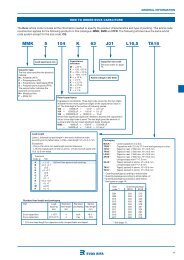
T491 SERIES - Precision Molded Chip<br />
• Meets or Exceeds EIA Standard 535BAAC<br />
• Taped and Reeled per EIA 481-1<br />
• Symmetrical, Compliant Terminations<br />
• Optional Gold-plated Terminations<br />
• Laser-marked Case<br />
• 100% Surge current test on C, D, E, U, V, X sizes<br />
• Halogen Free Epoxy<br />
• Capacitance: 0.1 F to 1000 F<br />
CATHODE (-) END<br />
VIEW<br />
W<br />
CAPACITOR OUTLINE DRAWING<br />
SIDE VIEW<br />
FEATURES<br />
B<br />
B<br />
• Tolerance: ±10%, ±20%<br />
• Voltage: 2.5-50 VDC<br />
• Extended Range Values<br />
• Low Profile Case Sizes<br />
• RoHS Compliance & Lead Free Terminations<br />
(See www.kemet.com for transition information)<br />
• Operating Temperature: -55˚C to +125˚C<br />
ANODE (+) END<br />
VIEW<br />
BOTTOM VIEW<br />
Solid Tantalum Surface Mount<br />
CASE SIZE<br />
KEMET EIA<br />
L* W* H*<br />
A<br />
B<br />
C<br />
D<br />
X<br />
E<br />
3216-18<br />
3528-21<br />
6032-28<br />
7343-31<br />
7343-43<br />
7260-38<br />
K<br />
X<br />
3.2 ± 0.2<br />
(.126 ± .008)<br />
3.5 ± 0.2<br />
(.138 ± .008)<br />
6.0 ± 0.3<br />
(.236 ± .012)<br />
7.3 ± 0.3<br />
(.287 ± .012)<br />
7.3 ± 0.3<br />
(.287 ± .012)<br />
7.3 ± 0.3<br />
(.287 ± .012)<br />
1.6 ±0.2<br />
(.063 ±.008)<br />
2.8 ± 0.2<br />
(.110 ± .008)<br />
3.2 ± 0.3<br />
(.126 ± .012)<br />
4.3 ± 0.3<br />
(.169 ± .012)<br />
4.3 ± 0.3<br />
(.169 ± .012)<br />
6.0 ± 0.3<br />
(.236 ± .012)<br />
CASE SIZE<br />
KEMET EIA L<br />
R 2012-12 2.0 ± 0.2<br />
(.079 ± .008)<br />
S 3216-12 3.2 ± 0.2<br />
(.126 .008)<br />
T<br />
3528-12 3.5 ± 0.2<br />
(.138 ± .008)<br />
U<br />
6032-15 6.0 0.3<br />
(.236 .012)<br />
V<br />
7343-20 7.3 ± 0.3<br />
(.287 ± .012)<br />
1.6 ± 0.2<br />
(.063 ± .008)<br />
1.9 ± 0.2<br />
(.075 ± .008)<br />
2.5 ± 0.3<br />
(.098 ± .012)<br />
2.8 ± 0.3<br />
(.110 ± .012)<br />
4.0 ± 0.3<br />
(.157 ± .012)<br />
3.6 ± 0.2<br />
(.142 ± .008)<br />
W<br />
1.3 ± 0.2<br />
(.051 ± .008)<br />
1.6 ± 0.2<br />
2.8 ± 0.2<br />
(.1 ± .008)<br />
4.3 ± 0.3<br />
(.169 ± .012)<br />
K* ± 0.20<br />
0.9<br />
(.035)<br />
1.1<br />
(.043)<br />
1.4<br />
(.055)<br />
1.5<br />
(.059)<br />
2.3<br />
(.091)<br />
2.3<br />
(.091)<br />
Notes: 1. Metric dimensions govern.<br />
2. (Ref) - Dimensions provided for reference only.<br />
* Mil-C-55365/8 Specified Dimensions<br />
H Max.<br />
1.2<br />
(.047)<br />
1.2<br />
(.047)<br />
1.2<br />
(.047)<br />
1.5<br />
(.059)<br />
2.0<br />
(.079)<br />
COMPONENT<br />
F* ± 0.1<br />
± (.004)<br />
1.2<br />
(.047)<br />
2.2<br />
(.087)<br />
2.2<br />
(.087)<br />
2.4<br />
(.094)<br />
2.4<br />
(.094)<br />
4.1<br />
(.161)<br />
± (.008)<br />
S* ± 0.3<br />
COMPONENT<br />
K Min. F ± 0.1 S ± 0.3<br />
0.3<br />
(.012)<br />
0.3<br />
(.012)<br />
0.3<br />
(.012)<br />
0.5<br />
(.020)<br />
0.9<br />
(.035)<br />
± (.012)<br />
0.8<br />
(.031)<br />
0.8<br />
(.031)<br />
1.3<br />
(.051)<br />
1.3<br />
(.051)<br />
1.3<br />
(.051)<br />
1.3<br />
(.051)<br />
0.9<br />
(.035)<br />
1.2<br />
(.047)<br />
2.2<br />
(.087)<br />
2.2<br />
(.087)<br />
2.4<br />
(.094)<br />
0.5<br />
(.020)<br />
0.8<br />
(.031)<br />
0.8<br />
(.031)<br />
1.3<br />
(.051)<br />
1.3<br />
(.051)<br />
0.10 ± 0.10<br />
(.004 ± .004)<br />
0.10 ± 0.10<br />
(.004 ± .004)<br />
0.10 ± 0.10<br />
(.004 ± .004)<br />
0.10 ± 0.10<br />
(.004 ± .004)<br />
0.10 ± 0.10<br />
(.004 ± .004)<br />
0.10 ± 0.10<br />
(.004 ± .004)<br />
X<br />
(Ref)<br />
0.05<br />
(.002)<br />
0.05<br />
(.002)<br />
0.05<br />
(.002)<br />
0.05<br />
(.002)<br />
0.05<br />
(.002)<br />
T<br />
(Ref)<br />
0.13<br />
(.005)<br />
0.13<br />
(.005)<br />
0.13<br />
(.005)<br />
0.13<br />
(.005)<br />
0.13<br />
(.005)<br />
Notes: 1. Metric dimensions govern.<br />
.<br />
3. No dimensions provided for B, P or R because low profile cases do not have a bevel or a notch.<br />
Tantalum<br />
Series<br />
T491 - Precision Molded<br />
Case Size<br />
A,B,C,D,E,R,S,T,U,V,X<br />
Capacitance Picofarad Code<br />
First two digits represent significant figures.<br />
Third digit specifies number of zeros to follow.<br />
H<br />
S<br />
T<br />
G<br />
S<br />
Termination<br />
cutout at<br />
KEMET’s<br />
Option,<br />
either end<br />
STANDARD T491 DIMENSIONS<br />
Millimeters (inches)<br />
B ± 0.15<br />
(Ref) ± (.006)<br />
©KEMET Electronics Corporation, P.O. Box 5928, Greenville, S.C. 29606, (864) 963-6300 15<br />
0.4<br />
(.016)<br />
0.4<br />
(.016)<br />
0.5<br />
(.020)<br />
0.5<br />
(.020)<br />
0.5<br />
(.020)<br />
0.5<br />
(.020)<br />
X<br />
(Ref)<br />
LOW PROFILE T491 DIMENSIONS<br />
Millimeters (inches)<br />
T491 ORDERING INFORMATION<br />
T 491 B 105 M 035 A S*<br />
*Part number example: T491B105M035AT (14 digits - no spaces). See www.kemet.com for Pb Free transition.<br />
** “S” Termination codes are converting from 90Sn/10 Pb to 100% tin finishes. Orders including “S” suffix<br />
termination codes do not quarantee Pb-free product.<br />
R<br />
P<br />
E<br />
A<br />
L<br />
P<br />
(Ref)<br />
0.4<br />
(.016)<br />
0.5<br />
(.020)<br />
0.9<br />
(.035)<br />
0.9<br />
(.035)<br />
1.7<br />
(.067)<br />
0.9<br />
(.035)<br />
F<br />
R<br />
(Ref)<br />
0.4<br />
(.016)<br />
1.0<br />
(.039)<br />
1.0<br />
(.039)<br />
1.0<br />
(.039)<br />
1.0<br />
(.039)<br />
1.0<br />
(.039)<br />
A<br />
(Min)<br />
0.8<br />
(.031)<br />
1.4<br />
(.055)<br />
2.1<br />
(.083)<br />
3.1<br />
(.122)<br />
3.8<br />
(.150)<br />
T<br />
(Ref)<br />
0.13<br />
(.005)<br />
0.13<br />
(.005)<br />
0.13<br />
(.005)<br />
0.13<br />
(.005)<br />
0.13<br />
(.005)<br />
0.13<br />
(.005)<br />
A<br />
(Min)<br />
1.4<br />
(.055)<br />
2.1<br />
(.083)<br />
3.1<br />
(.122)<br />
3.8<br />
(.150)<br />
3.8<br />
(.150)<br />
3.8<br />
(.150)<br />
G<br />
(Ref)<br />
0.5<br />
(.020)<br />
1.1<br />
(.043)<br />
1.8<br />
(.071)<br />
2.8<br />
(.110)<br />
3.5<br />
(.138)<br />
G<br />
(Ref)<br />
1.1<br />
(.043)<br />
1.8<br />
(.071)<br />
2.8<br />
(.110)<br />
3.5<br />
(.138)<br />
3.5<br />
(.138)<br />
3.5<br />
(.138)<br />
E<br />
(Ref)<br />
0.8<br />
(.031)<br />
1.3<br />
(.051)<br />
2.2<br />
(.087)<br />
2.4<br />
(.094)<br />
3.5<br />
(.138)<br />
T = 100% Tin (Sn) Plated<br />
H = Tin/Lead (SnPb 5% Pb minimum)<br />
G = Gold Plated (A,B,C,D,X only)<br />
**S = Not recommended for new designs<br />
E<br />
(Ref)<br />
1.3<br />
(.051)<br />
2.2<br />
(.087)<br />
2.4<br />
(.094)<br />
3.5<br />
(.138)<br />
3.5<br />
(.138)<br />
3.5<br />
(.138)<br />
Lead Material<br />
Failure Rate<br />
A = Not Applicable<br />
Voltage<br />
As shown<br />
Capacitance Tolerance<br />
M = ±20%; K = ±10%
SOLID TANTALUM CHIP CAPACITORS<br />
T491 SERIES—Precision Molded Chip<br />
T491 TANTALUM CHIP CAPACITANCE VALUES<br />
Case Size by Capacitance and Voltage<br />
Capacitance<br />
Rated Voltage @ +85°C<br />
µF Code 2.5 3 4 6 10 16 20 25 35 50<br />
0.10 104 A A<br />
0.15 154 A A/B<br />
0.22 224 A B<br />
0.33 334 A A B<br />
0.47 474 A A/B B/C<br />
0.68 684 A A A/B B/C<br />
1.0 105 A R/S/A A/B A/B V/C<br />
1.5 155 A A S/A A/B B/C C/D<br />
2.2 225 R/A A/B R/S/A A/B B/C B/C C/D<br />
3.3 335 A A R/S/A A/B T/A/B B/C B/C D<br />
4.7 475 A S/A<br />
6.8 685 S/A<br />
10.0 106<br />
15.0 156<br />
22.0 226<br />
33.0 336 A<br />
47.0 476<br />
68.0 686<br />
100.0 107 T<br />
150.0 157<br />
R/S<br />
A/B<br />
S/T<br />
A/B<br />
S/T<br />
A/B/C<br />
T/U<br />
A/B/C<br />
T/U<br />
A/B/C<br />
U/A<br />
B/C/D<br />
T/U/A<br />
B/C/D<br />
V/B<br />
C/D<br />
220.0 227 V/B<br />
R/S<br />
A/B<br />
R/S/T<br />
A/B<br />
S/T<br />
A/B/C<br />
U/T<br />
A/B/C<br />
T/U<br />
A/B/C<br />
T/U/A<br />
B/C/D<br />
U/B<br />
C/D<br />
U/V<br />
B/C/D<br />
V/C/D<br />
V/C<br />
D/X<br />
A/B<br />
R/S<br />
S/T<br />
A/B<br />
S/T/A<br />
B/C<br />
T/U<br />
A/B/C<br />
T/U<br />
A/B/C<br />
U/V<br />
B/C/D<br />
U/V<br />
B/C/D<br />
U/V<br />
B/C/D<br />
A/B/T A/B/C A/B/C C/D D<br />
A/B/C U/A/B/C B/C C/D D/X<br />
B/C/U<br />
T/A<br />
U/B/C C/D V/C/D D/X<br />
U/B/C C/D C/D D/X X<br />
U/B<br />
C/D<br />
V/C/D V/C/D D/X<br />
U/C/D V/C/D D/X X<br />
V/C/D D C/D/X X/E<br />
V/D D/X X<br />
V/C/D V/D/X X/E<br />
V/C<br />
D/X<br />
V/D/X<br />
D/X<br />
X/E<br />
X<br />
330.0 337 V/C/D D/X/E D/X/E<br />
470.0 477 D/X D/X/E X/E<br />
680.0 687 D/X E<br />
1000.0 108 X/E<br />
16<br />
©KEMET Electronics Corporation, P.O. Box 5928, Greenville, S.C. 29606, (864) 963-6300
Capacitance<br />
µF<br />
Case<br />
Size<br />
SOLID TANTALUM CHIP CAPACITORS<br />
T491 SERIES - Precision Molded Chip<br />
KEMET<br />
Part Number<br />
T491 RATINGS & PART NUMBER REFERENCE<br />
DC<br />
Leakage<br />
A @ 25ºC<br />
Max<br />
DF %<br />
@ +25ºC<br />
120 Hz<br />
Max<br />
ESR <br />
@ +25°C<br />
100 kHz<br />
Max<br />
2.5 Volt Rating at +85ºC (1.7 Volt Rating at +125ºC)<br />
100.0 T T491T107(1)2R5A(2) 2.5 24.0 3.9<br />
220.0 D T491D227(1)2R5A(2) 5.5 8.0 0.3<br />
3 Volt Rating at +85ºC (2 Volt Rating at +125ºC)<br />
#33.0 *A T491A336(1)003A(2) 1.0 6.0 4.0<br />
4 Volt Rating at +85ºC (2.7 Volt Rating at +125ºC)<br />
3.3 A T491A335(1)004A(2) 0.5 6.0 8.0<br />
4.7 A T491A475(1)004A(2) 0.5 6.0 8.0<br />
6.8 A T491A685(1)004A(2) 0.5 6.0 6.0<br />
6.8 S T491S685(1)004A(2) 0.5 6.0 15.0<br />
10.0 B T491B106(1)004A(2) 0.5 6.0 3.5<br />
10.0 A T491A106(1)004A(2) 0.5 6.0 6.0<br />
#10.0 *S T491S106(1)004A(2) 0.5 6.0 15.0<br />
#10.0 *R T491R106(1)004A(2) 0.5 8.0 10.0<br />
15.0 B T491B156(1)004A(2) 0.6 6.0 3.5<br />
15.0 A T491A156(1)004A(2) 0.6 6.0 4.0<br />
15.0 T T491T156(1)004A(2) 0.6 6.0 5.0<br />
#15.0 *S T491S156(1)004A(2) 0.6 10.0 15.0<br />
22.0 C T491C226(1)004A(2) 0.9 6.0 1.8<br />
22.0 B T491B226(1)004A(2) 0.9 6.0 3.5<br />
#22.0 A T491A226(1)004A(2) 0.9 6.0 4.0<br />
#22.0 *T T491T226(1)004A(2) 0.9 6.0 5.0<br />
22.0 *S T491S226(1)004A(2) 0.9 10.0 10.0<br />
33.0 C T491C336(1)004A(2) 1.3 6.0 1.8<br />
33.0 U T491U336(1)004A(2) 1.3 6.0 1.8<br />
33.0 B T491B336(1)004A(2) 1.3 6.0 3.5<br />
#33.0 A T491A336(1)004A(2) 1.3 6.0 4.0<br />
#33.0 *T T491T336(1)004A(2) 1.3 8.0 5.0<br />
47.0 C T491C476(1)004A(2) 1.9 6.0 1.8<br />
47.0 U T491U476(1)004A(2) 1.9 6.0 1.8<br />
#47.0 B T491B476(1)004A(2) 1.9 6.0 3.0<br />
#47.0 A T491A476M004A(2) 1.9 12.0 2.5<br />
#47.0 *T T491T476M004A(2) 1.9 12.0 6.0<br />
68.0 D T491D686(1)004A(2) 2.7 6.0 0.8<br />
68.0 C T491C686(1)004A(2) 2.7 6.0 1.6<br />
#68.0 *U T491U686(1)004A(2) 2.7 6.0 1.8<br />
#68.0 B T491B686(1)004A(2) 2.7 6.0 3.5<br />
#68.0 *A T491A686(1)004A(2) 2.8 30.0 4.0<br />
100.0 D T491D107(1)004A(2) 4.0 8.0 0.8<br />
#100.0 C T491C107(1)004A(2) 4.0 8.0 1.2<br />
#100.0 *U T491U107(1)004A(2) 4.0 10.0 1.8<br />
#100.0 *B T491B107M004A(2) 4.0 8.0 0.9<br />
†100.0 *A T491A107M004A(2) 4.0 30.0 4.0<br />
†100.0 *T T491T107M004A(2) 4.0 30.0 5.0<br />
150.0 D T491D157(1)004A(2) 6.0 8.0 0.8<br />
150.0 V T491V157(1)004A(2) 6.0 8.0 0.7<br />
#150.0 *C T491C157(1)004A(2) 6.0 8.0 1.2<br />
†150.0 *B T491B157M004A(2) 6.0 12.0 2.0<br />
#220.0 *V T491V227(1)004A(2) 8.8 8.0 0.7<br />
#220.0 *B T491B227M004A(2) 8.8 18.0 0.5<br />
330.0 D T491D337(1)004A(2) 13.2 8.0 0.7<br />
†330.0 *V T491V337(1)004A(2) 13.2 12.0 0.7<br />
#330.0 *C T491C337(1)004A(2) 13.2 10.0 0.9<br />
#470.0 X T491X477(1)004A(2) 18.8 8.0 0.5<br />
#470.0 *D T491D477(1)004A(2) 18.8 8.0 0.8<br />
#680.0 *X T491X687M004A(2) 27.2 12.0 0.5<br />
#680.0 *D T491D687M004A(2) 27.2 12.0 0.5<br />
#1000.0 *X T491X108(1)004A(2) 40.0 12.0 0.5<br />
#1000.0 *E T491E108M004A(2) 40.0 15.0 0.2<br />
**6 Volt Rating at +85ºC (4 Volt Rating at +125ºC)<br />
2.2 R T491R225(1)006A(2) 0.5 6.0 25.0<br />
2.2 A T491A225(1)006A(2) 0.5 6.0 8.0<br />
3.3 A T491A335(1)006A(2) 0.5 6.0 8.0<br />
4.7 A T491A475(1)006A(2) 0.5 6.0 6.0<br />
4.7 S T491S475(1)006A(2) 0.5 6.0 15.0<br />
6.8 B T491B685(1)006A(2) 0.5 6.0 3.5<br />
6.8 A T491A685(1)006A(2) 0.5 6.0 6.0<br />
#6.8 S T491S685(1)006A(2) 0.5 6.0 15.0<br />
#6.8 *R T491R685(1)006A(2) 0.5 8.0 15.0<br />
10.0 B T491B106(1)006A(2) 0.6 6.0 3.5<br />
10.0 A T491A106(1)006A(2) 0.6 6.0 4.0<br />
10.0 T T491T106(1)006A(2) 0.6 6.0 5.0<br />
#10.0 *S T491S106(1)006A(2) 0.6 10.0 15.0<br />
#10.0 *R T491R106(1)006A(2) 0.6 8.0 10.0<br />
Capacitance<br />
µF<br />
Case<br />
Size<br />
(1) To complete KEMET Part Number, insert M for ±20% tolerance or K for ±10% tolerance.<br />
(2) To complete KEMET Part Number, insert T, H, G, or S lead material designation as shown on page 15.<br />
*Extended Values<br />
**6 Volt product equivalent to 6.3 volt product.<br />
#Maximum Capacitance Change @ 125ºC=+15%.<br />
†Maximum Capacitance Change @ 125ºC=+20%.<br />
Higher voltage ratings and tighter tolerance product may be substituted within the same size at KEMET’s option.<br />
Voltage substitutions will be marked with the higher voltage rating.<br />
KEMET<br />
Part Number<br />
DC<br />
Leakage<br />
A @ 25ºC<br />
Max<br />
DF %<br />
@ +25ºC<br />
120 Hz<br />
Max<br />
ESR <br />
@ +25°C<br />
100 kHz<br />
Max<br />
**6 Volt Rating at +85ºC (4 Volt Rating at +125ºC)<br />
15.0 C T491C156(1)006A(2) 0.9 6.0 1.8<br />
15.0 B T491B156(1)006A(2) 0.9 6.0 3.5<br />
#15.0 A T491A156(1)006A(2) 0.9 6.0 3.5<br />
#15.0 T T491T156(1)006A(2) 0.9 6.0 5.0<br />
#15.0 *S T491S156(1)006A(2) 0.9 15.0 10.0<br />
22.0 C T491C226(1)006A(2) 1.4 6.0 1.8<br />
22.0 U T491U226(1)006A(2) 1.4 6.0 1.8<br />
22.0 B T491B226(1)006A(2) 1.4 6.0 3.5<br />
#22.0 A T491A226(1)006A(2) 1.4 6.0 4.0<br />
#22.0 T T491T226(1)006A(2) 1.4 8.0 5.0<br />
33.0 C T491C336(1)006A(2) 2.0 6.0 1.8<br />
33.0 U T491U336(1)006A(2) 2.0 6.0 1.8<br />
#33.0 B T491B336(1)006A(2) 2.0 6.0 3.0<br />
#33.0 A T491A336(1)006A(2) 2.0 12.0 2.5<br />
#33.0 *T T491T336(1)006A(2) 2.0 12.0 6.0<br />
47.0 D T491D476(1)006A(2) 2.9 6.0 0.8<br />
47.0 C T491C476(1)006A(2) 2.9 6.0 1.6<br />
#47.0 U T491U476(1)006A(2) 2.9 6.0 1.8<br />
#47.0 B T491B476(1)006A(2) 2.9 6.0 2.0<br />
†47.0 *A T491A476M006A(2) 3.0 12.0 3.5<br />
*47.0 *T T491T476(1)006A(2) 3.0 24.0 4.4<br />
68.0 D T491D686(1)006A(2) 4.1 6.0 0.8<br />
#68.0 C T491C686(1)006A(2) 4.1 6.0 1.2<br />
#68.0 *U T491U686(1)006A(2) 4.1 10.0 1.8<br />
#68.0 *B T491B686(1)006A(2) 4.1 8.0 0.9<br />
#68.0 *A T491A686(1)006A(2) 5.0 30.0 4.0<br />
100.0 D T491D107(1)006A(2) 6.0 8.0 0.8<br />
100.0 V T491V107(1)006A(2) 6.0 8.0 0.7<br />
#100.0 C T491C107(1)006A(2) 6.0 8.0 0.9<br />
#100.0 *U T491U107(1)006A(2) 6.0 10.0 1.8<br />
#100.0 *B T491B107(1)006A(2) 6.3 15.0 3.0<br />
150.0 D T491D157(1)006A(2) 9.0 8.0 0.7<br />
#150.0 *C T491C157(1)006A(2) 9.0 8.0 1.2<br />
#150.0 *V T491V157(1)006A(2) 9.0 8.0 0.7<br />
220.0 X T491X227(1)006A(2) 13.2 8.0 0.7<br />
#220.0 D T491D227(1)006A(2) 13.2 8.0 0.7<br />
#220.0 *C T491C227M006A(2) 13.2 10.0 1.2<br />
#220.0 *V T491V227(1)006A(2) 13.2 12.0 0.7<br />
330.0 *X T491X337(1)006A(2) 19.8 8.0 0.4<br />
330.0 *D T491D337(1)006A(2) 19.8 8.0 0.4<br />
330.0 *E T491E337(1)006A(2) 20.8 8.0 0.5<br />
470.0 *X T491X477(1)006A(2) 28.2 10.0 0.4<br />
470.0 *D T491D477M006A(2) 28.2 12.0 0.4<br />
470.0 *E T491E477(1)006A(2) 29.6 10.0 0.4<br />
680.0 *E T491E687M006A(2) 40.8 12.0 0.5<br />
10 Volt Rating at +85ºC (7 Volt Rating at +125ºC)<br />
1.5 A T491A155(1)010A(2) 0.5 6.0 8.0<br />
2.2 B T491B225(1)010A(2) 0.5 6.0 3.5<br />
2.2 A T491A225(1)010A(2) 0.5 6.0 8.0<br />
3.3 A T491A335(1)010A(2) 0.5 6.0 6.0<br />
3.3 S T491S335(1)010A(2) 0.5 6.0 15.0<br />
#3.3 *R T491R335(1)010A(2) 0.3 8.0 15.0<br />
4.7 B T491B475(1)010A(2) 0.5 15.0 3.5<br />
4.7 A T491A475(1)010A(2) 0.5 6.0 5.0<br />
#4.7 S T491S475(1)010A(2) 0.5 6.0 15.0<br />
#4.7 *R T491R475(1)010A(2) 0.5 8.0 10.0<br />
6.8 B T491B685(1)010A(2) 0.7 6.0 3.5<br />
6.8 A T491A685(1)010A(2) 0.7 6.0 4.0<br />
6.8 T T491T685(1)010A(2) 0.7 6.0 5.0<br />
#6.8 *S T491S685(1)010A(2) 0.7 10.0 15.0<br />
10.0 C T491C106(1)010A(2) 1.0 6.0 1.8<br />
10.0 B T491B106(1)010A(2) 1.0 6.0 3.5<br />
#10.0 A T491A106(1)010A(2) 1.0 6.0 4.0<br />
#10.0 T T491T106(1)010A(2) 1.0 6.0 5.0<br />
#10.0 *S T491S106(1)010A(2) 1.0 10.0 15.0<br />
15.0 C T491C156(1)010A(2) 1.5 6.0 1.8<br />
15.0 U T491U156(1)010A(2) 1.5 6.0 1.8<br />
15.0 B T491B156(1)010A(2) 1.5 6.0 2.8<br />
#15.0 *A T491A156(1)010A(2) 1.5 8.0 6.0<br />
#15.0 *T T491T156(1)010A(2) 1.5 8.0 5.0<br />
Solid Tantalum Surface Mount<br />
©KEMET Electronics Corporation, P.O. Box 5928, Greenville, S.C. 29606, (864) 963-6300 17
SOLID TANTALUM CHIP CAPACITORS<br />
T491 SERIES—Precision Molded Chip<br />
Capacitance<br />
µF<br />
Case<br />
Size<br />
T491 RATINGS & PART NUMBER REFERENCE<br />
KEMET<br />
Part Number<br />
DC<br />
Leakage<br />
A @ 25ºC<br />
Max<br />
DF %<br />
@ +25ºC<br />
120 Hz<br />
Max<br />
ESR <br />
@ +25°C<br />
100 kHz<br />
Max<br />
10 Volt Rating at +85ºC (7 Volt Rating at +125ºC)<br />
22.0 C T491C226(1)010A(2) 2.2 6.0 1.8<br />
22.0 U T491U226(1)010A(2) 2.2 6.0 1.8<br />
#22.0 B T491B226(1)010A(2) 2.2 6.0 2.4<br />
#22.0 *A T491A226M010A(2) 2.2 10.0 6.0<br />
#22.0 *T T491T226(1)010A(2) 2.2 12.0 8.0<br />
33.0 D T491D336(1)010A(2) 3.3 6.0 0.8<br />
33.0 V T491V336(1)010A(2) 3.3 6.0 0.7<br />
33.0 C T491C336(1)010A(2) 3.3 6.0 1.6<br />
#33.0 U T491U336(1)010A(2) 3.3 6.0 1.8<br />
#33.0 B T491B336(1)010A(2) 3.3 6.0 1.8<br />
47.0 D T491D476(1)010A(2) 4.7 6.0 0.8<br />
47.0 V T491V476(1)010A(2) 4.7 6.0 0.7<br />
#47.0 C T491C476(1)010A(2) 4.7 6.0 1.2<br />
#47.0 *U T491U476(1)010A(2) 4.7 10.0 2.2<br />
#47.0 *B T491B476(1)010A(2) 4.7 8.0 1.0<br />
68.0 D T491D686(1)010A(2) 6.8 6.0 0.8<br />
68.0 V T491V686(1)010A(2) 6.8 6.0 0.7<br />
#68.0 C T491C686(1)010A(2) 6.8 6.0 1.2<br />
#68.0 *U T491U686(1)010A(2) 6.8 10.0 1.8<br />
#68.0 *B T491B686M010A(2) 6.8 10.0 3.0<br />
100.0 D T491D107(1)010A(2) 10.0 8.0 0.7<br />
#100.0 *C T491C107(1)010A(2) 10.0 8.0 1.2<br />
#100.0 V T491V107(1)010A(2) 10.0 8.0 0.7<br />
150.0 X T491X157(1)010A(2) 15.0 8.0 0.7<br />
#150.0 D T491D157(1)010A(2) 15.0 8.0 0.7<br />
#150.0 *C T491C157(1)010A(2) 15.0 10.0 0.9<br />
#150.0 *V T491V157(1)010A(2) 15.0 8.0 0.7<br />
#220.0 X T491X227(1)010A(2) 22.0 8.0 0.5<br />
#220.0 *D T491D227(1)010A(2) 22.0 8.0 0.5<br />
#220.0 *V T491V227(1)010A(2) 22.0 12.0 0.7<br />
#330.0 *D T491D337M010A(2) 33.0 10.0 0.5<br />
#330.0 *X T491X337(1)010A(2) 33.0 10.0 0.5<br />
#330.0 *E T491E337(1)010A(2) 33.0 10.0 0.5<br />
#470.0 *X T491X477(1)010A(2) 47.0 10.0 0.2<br />
#470.0 *E T491E477M010A(2) 47.0 12.0 0.5<br />
16 Volt Rating at +85ºC (10 Volt Rating at +125ºC)<br />
1.0 A T491A105(1)016A(2) 0.5 4.0 10.0<br />
1.5 A T491A155(1)016A(2) 0.5 6.0 8.0<br />
2.2 A T491A225(1)016A(2) 0.5 6.0 6.0<br />
2.2 *S T491S225(1)016A(2) 0.5 6.0 15.0<br />
#2.2 *R T491R225(1)016A(2) 0.5 8.0 25.0<br />
3.3 B T491B335(1)016A(2) 0.5 6.0 3.5<br />
3.3 A T491A335(1)016A(2) 0.5 6.0 5.0<br />
4.7 B T491B475(1)016A(2) 0.8 6.0 3.5<br />
4.7 A T491A475(1)016A(2) 0.8 6.0 4.0<br />
4.7 T T491T475(1)016A(2) 0.8 6.0 5.0<br />
6.8 C T491C685(1)016A(2) 1.1 6.0 1.9<br />
6.8 B T491B685(1)016A(2) 1.1 6.0 2.5<br />
#6.8 *A T491A685(1)016A(2) 1.1 6.0 3.5<br />
10.0 C T491C106(1)016A(2) 1.6 6.0 1.8<br />
10.0 U T491U106(1)016A(2) 1.6 6.0 1.8<br />
10.0 B T491B106(1)016A(2) 1.6 6.0 2.8<br />
#10.0 *A T491A106(1)016A(2) 1.6 8.0 7.0<br />
#10.0 *T T491T106(1)016A(2) 1.6 8.0 8.0<br />
15.0 C T491C156(1)016A(2) 2.4 6.0 1.8<br />
15.0 U T491U156(1)016A(2) 2.4 6.0 1.8<br />
#15.0 *B T491B156(1)016A(2) 2.4 6.0 2.5<br />
22.0 D T491D226(1)016A(2) 3.6 6.0 0.8<br />
22.0 C T491C226(1)016A(2) 3.6 6.0 1.6<br />
#22.0 *U T491U226(1)016A(2) 3.6 10.0 3.0<br />
#22.0 *B T491B226(1)016A(2) 3.6 6.0 2.2<br />
33.0 D T491D336(1)016A(2) 5.3 6.0 0.8<br />
#33.0 *C T491C336(1)016A(2) 5.3 6.0 1.2<br />
#33.0 *U T491U336(1)016A(2) 5.3 12.0 3.0<br />
47.0 D T491D476(1)016A(2) 7.5 6.0 0.8<br />
47.0 V T491V476(1)016A(2) 7.5 6.0 0.7<br />
#47.0 *C T491C476(1)016A(2) 7.5 6.0 1.2<br />
68.0 *V T491V686(1)016A(2) 10.9 6.0 0.7<br />
68.0 D T491D686(1)016A(2) 10.9 6.0 0.7<br />
Capacitance<br />
µF<br />
Case<br />
Size<br />
(1) To complete KEMET Part Number, insert M for ±20% tolerance or K for ±10% tolerance.<br />
(2) To complete KEMET Part Number, insert T, H, G, or S lead material designation as shown on page 15.<br />
*Extended Values<br />
**6 Volt product equivalent to 6.3 volt product.<br />
#Maximum Capacitance Change @ 125ºC=+15%.<br />
†Maximum Capacitance Change @ 125ºC=+20%.<br />
Higher voltage ratings and tighter tolerance product may be substituted within the same size at KEMET’s option.<br />
Voltage substitutions will be marked with the higher voltage rating.<br />
KEMET<br />
Part Number<br />
DC<br />
Leakage<br />
μA @ 25ºC<br />
Max<br />
DF %<br />
@ +25ºC<br />
120 Hz<br />
Max<br />
ESR Ω<br />
@ +25°C<br />
100 kHz<br />
Max<br />
16 Volt Rating at +85ºC (10 Volt Rating at +125ºC)<br />
100.0 X T491X107(1)016A(2) 16.0 8.0 0.7<br />
†100.0 *V T491V107(1)016A(2) 16.0 12.0 0.7<br />
#100.0 *D T491D107(1)016A(2) 16.0 8.0 0.7<br />
#150.0 *X T491X157(1)016A(2) 24.0 8.0 0.5<br />
#150.0 *D T491D157(1)016A(2) 24.0 12.0 0.7<br />
#220.0 *X T491X227(1)016A(2) 35.2 10.0 0.5<br />
#220.0 *E T491E227(1)016A(2) 35.2 7.2 0.9<br />
20 Volt Rating at +85ºC (13 Volt Rating at + 125ºC)<br />
0.68 A T491A684(1)020A(2) 0.5 4.0 12.0<br />
1.0 A T491A105(1)020A(2) 0.5 4.0 9.0<br />
1.0 S T491S105(1)020A(2) 0.5 6.0 18.0<br />
#1.0 R T491R105(1)020A(2) 0.5 6.0 20.0<br />
1.5 A T491A155(1)020A(2) 0.5 6.0 6.5<br />
1.5 S T491S155(1)020A(2) 0.5 6.0 15.0<br />
2.2 B T491B225(1)020A(2) 0.5 6.0 3.5<br />
2.2 A T491A225(1)020A(2) 0.5 6.0 7.0<br />
3.3 B T491B335(1)020A(2) 0.7 6.0 3.0<br />
#3.3 *A T491A335(1)020A(2) 0.7 6.0 4.5<br />
3.3 *T T491T335(1)020A(2) 0.7 6.0 5.0<br />
4.7 C T491C475(1)020A(2) 1.0 6.0 2.4<br />
4.7 B T491B475(1)020A(2) 1.0 6.0 3.0<br />
#4.7 *A T491A475(1)020A(2) 1.0 6.0 4.0<br />
6.8 C T491C685(1)020A(2) 1.4 6.0 1.9<br />
6.8 U T491U685(1)020A(2) 1.4 6.0 1.9<br />
#6.8 *B T491B685(1)020A(2) 1.4 6.0 2.5<br />
#6.8 *A T491A685M020A(2) 1.4 8.0 6.0<br />
10.0 C T491C106(1)020A(2) 2.0 6.0 1.8<br />
10.0 U T491U106(1)020A(2) 2.0 6.0 1.8<br />
#10.0 *B T491B106(1)020A(2) 2.0 6.0 2.1<br />
15.0 D T491D156(1)020A(2) 3.0 6.0 1.0<br />
15.0 C T491C156(1)020A(2) 3.0 6.0 1.7<br />
22.0 D T491D226(1)020A(2) 4.4 6.0 0.8<br />
22.0 V T491V226(1)020A(2) 4.4 6.0 0.7<br />
#22.0 *C T491C226(1)020A(2) 4.4 6.0 1.2<br />
33.0 D T491D336(1)020A(2) 6.6 6.0 0.8<br />
#33.0 *C T491C336M020A(2) 6.6 6.0 1.2<br />
†33.0 *V T491V336(1)020A(2) 6.6 8.0 0.7<br />
47.0 C T491C476M020A(2) 9.4 10.0 0.9<br />
47.0 *D T491D476(1)020A(2) 9.4 6.0 0.7<br />
68.0 X T491X686(1)020A(2) 13.6 6.0 0.7<br />
#68.0 *D T491D686(1)020A(2) 13.6 8.0 0.7<br />
#100.0 *X T491X107(1)020A(2) 20.0 8.0 0.5<br />
#100.0 *E T491E107(1)020A(2) 20.0 8.0 0.5<br />
#150.0 *X T491X157(1)020A(2) 30.0 10.0 0.5<br />
25 Volt Rating at +85ºC (17 Volt Rating at +125ºC)<br />
0.33 A T491A334(1)025A(2) 0.5 4.0 15.0<br />
0.47 A T491A474(1)025A(2) 0.5 4.0 14.0<br />
0.68 A T491A684(1)025A(2) 0.5 4.0 10.0<br />
1.0 B T491B105(1)025A(2) 0.5 4.0 5.0<br />
1.0 *A T491A105(1)025A(2) 0.5 4.0 8.0<br />
1.5 B T491B155(1)025A(2) 0.5 6.0 5.0<br />
1.5 *A T491A155(1)025A(2) 0.5 6.0 7.5<br />
2.2 C T491C225(1)025A(2) 0.6 6.0 3.5<br />
2.2 B T491B225(1)025A(2) 0.6 6.0 4.5<br />
3.3 C T491C335(1)025A(2) 0.9 6.0 2.5<br />
3.3 B T491B335(1)025A(2) 0.9 6.0 3.5<br />
4.7 C T491C475(1)025A(2) 1.2 6.0 2.4<br />
#4.7 *B T491B475(1)025A(2) 1.2 6.0 1.5<br />
#4.7 *A T491A475M025A(2) 1.2 8.0 6.0<br />
6.8 C T491C685(1)025A(2) 1.7 6.0 1.9<br />
6.8 *B T491B685(1)025A(2) 1.7 8.0 2.8<br />
10.0 D T491D106(1)025A(2) 2.5 6.0 1.0<br />
10.0 C T491C106(1)025A(2) 2.5 6.0 1.5<br />
15.0 D T491D156(1)025A(2) 3.8 6.0 1.0<br />
#15.0 *C T491C156(1)025A(2) 3.8 6.0 1.5<br />
22.0 D T491D226(1)025A(2) 5.5 6.0 0.8<br />
22.0 *C T491C226(1)025A(2) 5.5 6.0 1.4<br />
22.0 *V T491V226(1)025A(2) 5.5 6.0 0.7<br />
33.0 X T491X336(1)025A(2) 8.3 6.0 0.7<br />
#33.0 *D T491D336(1)025A(2) 8.3 6.0 0.7<br />
#47.0 *X T491X476(1)025A(2) 11.8 6.0 0.7<br />
†47.0 *D T491D476(1)025A(2) 11.8 10.0 0.7<br />
†68.0 *X T491X686M025A(2) 17.0 8.0 0.7<br />
18<br />
©KEMET Electronics Corporation, P.O. Box 5928, Greenville, S.C. 29606, (864) 963-6300
SOLID TANTALUM CHIP CAPACITORS<br />
T491 SERIES—Precision Molded Chip<br />
Capacitance<br />
µF<br />
Case<br />
Size<br />
T491 RATINGS & PART NUMBER REFERENCE<br />
KEMET<br />
Part Number<br />
DC<br />
Leakage<br />
A @ 25ºC<br />
Max<br />
DF %<br />
@ +25ºC<br />
120 Hz<br />
Max<br />
ESR <br />
@ +25°C<br />
100 kHz<br />
Max<br />
35 Volt Rating at +85ºC (23 Volt Rating at +125ºC)<br />
0.10 A T491A104(1)035A(2) 0.5 4.0 20.0<br />
0.15 A T491A154(1)035A(2) 0.5 4.0 19.0<br />
0.22 A T491A224(1)035A(2) 0.5 4.0 18.0<br />
0.33 A T491A334(1)035A(2) 0.5 4.0 15.0<br />
0.47 B T491B474(1)035A(2) 0.5 4.0 8.0<br />
0.47 A T491A474(1)035A(2) 0.5 4.0 12.0<br />
0.68 B T491B684(1)035A(2) 0.5 4.0 6.5<br />
0.68 *A T491A684(1)035A(2) 0.5 4.0 8.0<br />
1.0 B T491B105(1)035A(2) 0.5 4.0 5.0<br />
1.0 *A T491A105(1)035A(2) 0.5 4.0 7.5<br />
1.5 C T491C155(1)035A(2) 0.5 6.0 4.5<br />
1.5 B T491B155(1)035A(2) 0.5 6.0 5.0<br />
2.2 C T491C225(1)035A(2) 0.8 6.0 3.5<br />
2.2 *B T491B225(1)035A(2) 0.8 6.0 4.0<br />
3.3 C T491C335(1)035A(2) 1.2 6.0 2.5<br />
#3.3 *B T491B335(1)035A(2) 1.2 6.0 3.5<br />
4.7 D T491D475(1)035A(2) 1.7 6.0 1.5<br />
4.7 C T491C475(1)035A(2) 1.7 6.0 2.2<br />
6.8 D T491D685(1)035A(2) 2.4 6.0 1.3<br />
6.8 *C T491C685(1)035A(2) 2.4 6.0 1.8<br />
10.0 D T491D106(1)035A(2) 3.5 6.0 1.0<br />
#10.0 *C T491C106M035A(2) 3.5 6.0 1.6<br />
#10.0 *V T491V106(1)035A(2) 3.5 6.0 2.0<br />
15.0 X T491X156(1)035A(2) 5.3 6.0 0.9<br />
15.0 D T491D156(1)035A(2) 5.3 6.0 0.8<br />
22.0 X T491X226(1)035A(2) 7.7 6.0 0.7<br />
#22.0 *D T491D226(1)035A(2) 7.7 6.0 0.7<br />
#33.0 *X T491X336(1)035A(2) 11.6 6.0 0.6<br />
†47.0 *X T491X476(1)035A(2) 16.5 8.0 0.6<br />
#47.0 *E T491E476(1)035A(2) 16.5 10.0 0.5<br />
50 Volt Rating at +85ºC (33 Volt Rating at + 125ºC)<br />
0.10 A T491A104(1)050A(2) 0.5 4.0 20.0<br />
0.15 B T491B154(1)050A(2) 0.5 4.0 16.0<br />
0.15 *A T491A154(1)050A(2) 0.5 4.0 15.0<br />
0.22 B T491B224(1)050A(2) 0.5 4.0 14.0<br />
0.33 B T491B334(1)050A(2) 0.5 4.0 10.0<br />
0.47 C T491C474(1)050A(2) 0.5 4.0 8.0<br />
0.47 *B T491B474(1)050A(2) 0.5 4.0 9.0<br />
0.68 C T491C684(1)050A(2) 0.5 4.0 7.0<br />
0.68 *B T491B684(1)050A(2) 0.5 4.0 8.0<br />
1.0 C T491C105(1)050A(2) 0.5 4.0 5.5<br />
1.0 *V T491V105(1)050A(2) 0.5 4.0 6.0<br />
1.5 D T491D155(1)050A(2) 0.8 6.0 3.5<br />
1.5 *C T491C155(1)050A(2) 0.8 6.0 4.5<br />
2.2 D T491D225(1)050A(2) 1.1 6.0 2.5<br />
2.2 *C T491C225(1)050A(2) 1.1 6.0 3.0<br />
3.3 D T491D335(1)050A(2) 1.7 6.0 2.0<br />
4.7 D T491D475(1)050A(2) 2.4 6.0 1.4<br />
6.8 X T491X685(1)050A(2) 3.5 6.0 1.0<br />
#6.8 *D T491D685(1)050A(2) 3.4 6.0 1.0<br />
#10.0 *X T491X106M050A(2) 5.0 6.0 0.7<br />
#10.0 *D T491D106(1)050A(2) 5.0 6.0 0.8<br />
†15.0 *X T491X156(1)050A(2) 7.5 8.0 0.7<br />
Molded<br />
Case<br />
Tantalum<br />
(Ta 2O 5)<br />
Negative<br />
Termination*<br />
Mn02 Coat<br />
(First Layer)<br />
CONSTRUCTION<br />
Carbon<br />
(Second Layer)<br />
CAPACITOR MARKINGS<br />
T491 Series — All Case Sizes<br />
Rated<br />
Voltage<br />
Silver Adhesive<br />
Washer<br />
Silver Paint<br />
(Third Layer)<br />
226<br />
20K<br />
542<br />
Print Week Code:<br />
1st Digit = Year<br />
2nd & 3rd Digits = Week<br />
"542" = The 42nd week of 2005<br />
Polarity<br />
Indicator (+)<br />
Picofarad<br />
Code<br />
Polarity<br />
Stripe (+) Polarity<br />
Bevel (+)<br />
KEMET<br />
I. D. Symbol<br />
Positive<br />
Termination*<br />
*100% tin<br />
Tantalum<br />
Wire<br />
Weld<br />
Solid Tantalum Surface Mount<br />
(1) To complete KEMET Part Number, insert M for ±20% tolerance or K for ±10% tolerance.<br />
(2) To complete KEMET Part Number, insert T, H, G, or S lead material designation as shown on page 15.<br />
*Extended Values<br />
**6 Volt product equivalent to 6.3 volt product.<br />
#Maximum Capacitance Change @ 125ºC=+15%.<br />
†Maximum Capacitance Change @ 125ºC=+20%.<br />
Higher voltage ratings and tighter tolerance product may be substituted within the same size at KEMET’s option.<br />
Voltage substitutions will be marked with the higher voltage rating.<br />
©KEMET Electronics Corporation, P.O. Box 5928, Greenville, S.C. 29606, (864) 963-6300<br />
19
• Established reliability military version of<br />
Industrial Grade T491 series<br />
• Taped and reeled per EIA 481-1<br />
• Precision-molded, laser-marked case<br />
• Symmetrical, compliant terminations<br />
• 100% Surge Current test available for all case sizes<br />
• Operating Temperature: -55˚C to + 125˚C<br />
CASE SIZE<br />
SOLID TANTALUM CHIP CAPACITORS<br />
T492 SERIES—Style CWR11 Per Mil-PRF-55365/8<br />
K<br />
CATHODE (-) END<br />
VIEW<br />
X<br />
W<br />
H<br />
T492 OUTLINE DRAWINGS<br />
S<br />
T<br />
SIDE VIEW<br />
G<br />
B<br />
S<br />
B<br />
DIMENSIONS – Millimeters (Inches)<br />
• Qualified to MIL-PRF-55365/8, Style CWR11:<br />
– Termination Options B, C, H, K<br />
– Weibull failure rate codes B, C and D<br />
– Capacitance values and voltages as shown<br />
in following part number table. (Contact<br />
KEMET for latest qualification status)<br />
ANODE (+) END<br />
VIEW<br />
COMPONENT<br />
Termination<br />
cutout at<br />
KEMET’s<br />
Option,<br />
either end<br />
BOTTOM VIEW<br />
±0.20 ±-0.1 ±0.3 B ±0.15 X P R T A G E<br />
L* W* H* K* F* S*<br />
KEMET EIA<br />
±(.008) ±(.004) ±(.012) (Ref) ± (.006) (Ref) (Ref) (Ref) (Ref) (Min) (Ref) (Ref)<br />
A 3216-18 3.2 ± 0.2 1.6 ± 0.2 1.6 ± 0.2 0.9 1.2 0.8 0.4 0.10 ± 0.10 0.4 0.4 0.13 0.8 1.1 1.3<br />
(.126 ± .008) (.063 ± .008) (.063 ± .008) (.035) (.047) (.031) (.016) (.004 ± .004) (.016) (.016) (.005) (.031) (.043) (.051)<br />
B 3528-21 3.5 ± 0.2 2.8 ± 0.2 1.9 ± 0.2 1.1 2.2 0.8 0.4 0.10 ± 0.10 0.5 1.0 0.13 1.1 1.8 2.2<br />
(.138 ± .008) (.110 ± .008) (.075 ± .008) (.043) (.087) (.031) (.016) (.004 ± .004) (.020) (.039) (.005) (.043) (.071) (.087)<br />
C 6032-28 6.0 ± 0.3 3.2 ± 0.3 2.5 ± 0.3 1.4 2.2 1.3 0.5 0.10 ± 0.10 0.9 1.0 0.13 2.5 2.8 2.4<br />
(.236 ± .012) (.126 ± .012) (.098 ± .012) (.055) (.087) (.051) (.020) (.004 ± .004) (.035) (.039) (.005) (.098) (.110) (.094)<br />
D 7343-31 7.3 ± 0.3 4.3± 0.3 2.8 ± 0.3 1.5 2.4 1.3 0.5 0.10 ± 0.10 0.9 1.0 0.13 3.8 3.5 3.5<br />
(.287 ± .012) (.169 ± .012) (.110 ± .012) (.059) (.094) (.051) (.020) (.004 ± .004) (.035) (.039) (.005) (.150) (.138) (.138)<br />
R<br />
P<br />
E<br />
A<br />
L<br />
F<br />
Notes:<br />
1. Metric dimensions govern.<br />
2. (Ref) - Dimensions provided for reference only.<br />
* Mil-C-55365/8 Specified Dimensions<br />
ORDERING INFORMATION — MIL-PRF-55365 Part Number<br />
CWR11 M H 105 K B A<br />
Style<br />
Capacitors, Chip, Fixed Tantalum<br />
Established Reliability, (encapsulated)<br />
Voltage<br />
D = 6V J = 20V<br />
F = 10V K = 25V<br />
H = 15V M = 35V<br />
Termination Finish Code<br />
B = Gold Plated C = Hot Solder Dipped<br />
H = Solder Plated K = Solder Fused<br />
Capacitance Picofarad Code<br />
First two digits represent significant figures.<br />
Third digit specifies number of zeros to follow.<br />
T492 SERIES ORDERING INFORMATION — KEMET Part Number<br />
Tantalum<br />
Series<br />
T492 - Precision Molded, Style CWR11<br />
Case Size<br />
A, B, C, D<br />
Capacitance Picofarad Code<br />
First two digits represent significant figures.<br />
Third digit specifies number of zeros to follow.<br />
Capacitance Tolerances<br />
M = ±10%; K = ±10%; J = ±5%<br />
Voltage<br />
As shown<br />
# Inactive for<br />
New Design<br />
T 492 B 105 K 035 B S 4250<br />
Surge Current Option<br />
A = +25°C after Weibull<br />
B = -55°C +85°C after Weibull<br />
C = -55°, & +85°C before Weibull<br />
Z = None<br />
Failure Rate Symbol<br />
Weibull: B (0.1%/1000 hrs.)<br />
C (0.01%/1000 hrs.)<br />
D (0.001%/1000 hrs.)<br />
#Exponential:<br />
M (1.0%/1000 hrs.)<br />
P (0.1%/1000 hrs.)<br />
R (0.01%/1000 hrs.)<br />
S (0.001%/1000 hrs.)<br />
Capacitance Tolerances<br />
M = ±10%; K = ±10%; J = ±5%<br />
Surge Current Option<br />
4250 = +25°C after Weibull<br />
4251 = -55° +85°C after Weibull<br />
4252 = -55, & +85°C before Weibull<br />
Lead Material<br />
B = Gold<br />
C = Hot Solder Dip<br />
H or S = Solder Plated<br />
K = Solder Fused<br />
Failure Rate Symbol<br />
Weibull: B (0.1%/1000 hrs.); C (0.01%/1000 hrs.); D (0.001%/1000 hrs.)<br />
# Exponential: M (1.0%/1000 hrs.); P (0.1%/1000 hrs.), R (0.01%/1000 hrs.);<br />
S (0.001%/1000 hrs.) # Exponential not recommended for new design<br />
* Part Number Example: T492B105K035BS (14 digits - no spaces)<br />
* See www.kemet.com for Pb Free transition.<br />
20<br />
# Note on Failure Rates: Exponential failure rate levels M, P, R and S are inactive for new design per Mil-C-55365.<br />
Parts qualified to Weibull failure rate levels are substitutable for exponential failure rate levels.<br />
©KEMET Electronics Corporation, P.O. Box 5928, Greenville, S.C. 29606, (864) 963-6300
SOLID TANTALUM CHIP CAPACITORS<br />
T492 SERIES—Style CWR11 Per Mil-PRF-55365/8<br />
T492 (CWR11) RATINGS AND PART NUMBER REFERENCE<br />
ESR<br />
DC DCL DF DF % ESR<br />
Capaci-<br />
Capaci- Leakage % +25C @ +25C @<br />
Case<br />
KEMET<br />
Mil-C-55365/8 μA @ @ +25°C<br />
tance<br />
Case KEMET Mil-C-55365/8 A @ +25C 120 Hz 100kHz +25°C<br />
Size Part Number<br />
Part Number +25°C 120 Hz<br />
μF F Size Part Number Part Number Max Max Max 100kHz<br />
Max Max<br />
Max<br />
6 Volt Rating at +85°C (4 Volt Rating at +125°C)<br />
1.5 A T492A155(1)006(2)(3)(4) CWR11D(6)155(1)(2)(5) 0.5 6.0 8.0<br />
2.2 A T492A225(1)006(2)(3)(4) CWR11D(6)225(1)(2)(5) 0.5 6.0 8.0<br />
3.3 A T492A335(1)006(2)(3)(4) CWR11D(6)335(1)(2)(5) 0.5 6.0 ESR 8.0<br />
DCL DF %<br />
Capacitance<br />
6.8 B T492B685(1)006(2)(3)(4) CWR11D(6)685(1)(2)(5) 0.5 6.0 4.5<br />
4.7 B T492B475(1)006(2)(3)(4) CWR11D(6)475(1)(2)(5) 0.5 6.0 5.5<br />
Case<br />
KEMET<br />
Mil-C-55365/8 μA @ @ +25°C<br />
Size Part Number<br />
Part Number +25°C 120 Hz<br />
μF 10.0 B T492B106(1)006(2)(3)(4) CWR11D(6)106(1)(2)(5) 0.6 6.0 3.5<br />
Max Max<br />
15.0 C T492C156(1)006(2)(3)(4) CWR11D(6)156(1)(2)(5) 0.9 6.0 3.0<br />
22.0 C T492C226(1)006(2)(3)(4) CWR11D(6)226(1)(2)(5) 1.4 6.0 2.2<br />
47.0 D T492D476(1)006(2)(3)(4) CWR11D(6)476(1)(2)(5) 2.8 6.0 1.1<br />
10 Volt Rating at +85°C (7 Volt Rating at 125°C)<br />
1.0 A T492A105(1)010(2)(3)(4) CWR11F(6)105(1)(2)(5) 0.5 4.0 10.0<br />
1.5 A T492A155(1)010(2)(3)(4) CWR11F(6)155(1)(2)(5) 0.5 6.0 8.0<br />
2.2 A T492A225(1)010(2)(3)(4) CWR11F(6)225(1)(2)(5) 0.5 6.0 8.0<br />
3.3 B T492B335(1)010(2)(3)(4) CWR11F(6)335(1)(2)(5) 0.5 6.0 5.5<br />
4.7 B T492B475(1)010(2)(3)(4) CWR11F(6)475(1)(2)(5) 0.5 6.0 4.5<br />
6.8 B T492B685(1)010(2)(3)(4) CWR11F(6)685(1)(2)(5) 0.7 6.0 3.5<br />
15.0 C T492C156(1)010(2)(3)(4) CWR11F(6)156(1)(2)(5) 1.5 6.0 2.5<br />
33.0 D T492D336(1)010(2)(3)(4) CWR11F(6)336(1)(2)(5) 3.3 6.0 1.1<br />
15 Volt Rating at +85°C (10 Volt Rating at +125°C)<br />
0.7 A T492A684(1)015(2)(3)(4) CWR11H(6)684(1)(2)(5) 0.5 4.0 12.0<br />
1.0 A T492A105(1)015(2)(3)(4) CWR11H(6)105(1)(2)(5) 0.5 4.0 10.0<br />
1.5 A T492A155(1)015(2)(3)(4) CWR11H(6)155(1)(2)(5) 0.5 6.0 8.0<br />
2.2 B T492B225(1)015(2)(3)(4) CWR11H(6)225(1)(2)(5) 0.5 6.0 5.5<br />
3.3 B T492B335(1)015(2)(3)(4) CWR11H(6)335(1)(2)(5) 0.5 6.0 5.0<br />
4.7 B T492B475(1)015(2)(3)(4) CWR11H(6)475(1)(2)(5) 0.7 6.0 4.0<br />
10.0 C T492C106(1)015(2)(3)(4) CWR11H(6)106(1)(2)(5) 1.6 6.0 2.5<br />
22.0 D T492D226(1)015(2)(3)(4) CWR11H(6)226(1)(2)(5) 3.3 6.0 1.1<br />
20 Volt Rating at +85°C (13 Volt Rating at +125°C)<br />
0.5 A T492A474(1)020(2)(3)(4) CWR11J(6)474(1)(2)(5) 0.5 4.0 14.0<br />
0.7 A T492A684(1)020(2)(3)(4) CWR11J(6)684(1)(2)(5) 0.5 4.0 12.0<br />
1.0 A T492A105(1)020(2)(3)(4) CWR11J(6)105(1)(2)(5) 0.5 4.0 10.0<br />
1.5 B T492B155(1)020(2)(3)(4) CWR11J(6)155(1)(2)(5) 0.5 6.0 6.0<br />
2.2 B T492B225(1)020(2)(3)(4) CWR11J(6)225(1)(2)(5) 0.5 6.0 5.0<br />
3.3 B T492B335(1)020(2)(3)(4) CWR11J(6)335(1)(2)(5) 0.7 6.0 4.0<br />
4.7 C T492C475(1)020(2)(3)(4) CWR11J(6)475(1)(2)(5) 1.0 6.0 3.0<br />
6.8 C T492C685(1)020(2)(3)(4) CWR11J(6)685(1)(2)(5) 1.4 6.0 2.4<br />
15.0 D T492D156(1)020(2)(3)(4) CWR11J(6)156(1)(2)(5) 3.0 6.0 1.1<br />
25 Volt Rating at +85°C (17 Volt Rating at +125°C)<br />
0.3 A T492A334(1)025(2)(3)(4) CWR11K(6)334(1)(2)(5) 0.5 4.0 15.0<br />
0.5 A T492A474(1)025(2)(3)(4) CWR11K(6)474(1)(2)(5) 0.5 4.0 14.0<br />
0.7 B T492B684(1)025(2)(3)(4) CWR11K(6)684(1)(2)(5) 0.5 4.0 7.5<br />
1.0 B T492B105(1)025(2)(3)(4) CWR11K(6)105(1)(2)(5) 0.5 4.0 6.5<br />
1.5 B T492B155(1)025(2)(3)(4) CWR11K(6)155(1)(2)(5) 0.5 6.0 6.5<br />
2.2 C T492C225(1)025(2)(3)(4) CWR11K(6)225(1)(2)(5) 0.6 6.0 3.5<br />
3.3 C T492C335(1)025(2)(3)(4) CWR11K(6)335(1)(2)(5) 0.9 6.0 3.5<br />
4.7 C T492C475(1)025(2)(3)(4) CWR11K(6)475(1)(2)(5) 1.2 6.0 2.5<br />
6.8 D T492D685(1)025(2)(3)(4) CWR11K(6)685(1)(2)(5) 1.7 6.0 1.4<br />
10.0 D T492D106(1)025(2)(3)(4) CWR11K(6)106(1)(2)(5) 2.5 6.0 1.2<br />
35 Volt Rating at +85°C (23 Volt Rating at +125°C)<br />
0.1 A T492A104(1)035(2)(3)(4) CWR11M(6)104(1)(2)(5) 0.5 4.0 24.0<br />
0.2 A T492A154(1)035(2)(3)(4) CWR11M(6)154(1)(2)(5) 0.5 4.0 21.0<br />
0.2 A T492A224(1)035(2)(3)(4) CWR11M(6)224(1)(2)(5) 0.5 4.0 18.0<br />
0.3 A T492A334(1)035(2)(3)(4) CWR11M(6)334(1)(2)(5) 0.5 4.0 15.0<br />
0.5 B T492B474(1)035(2)(3)(4) CWR11M(6)474(1)(2)(5) 0.5 4.0 10.0<br />
0.7 B T492B684(1)035(2)(3)(4) CWR11M(6)684(1)(2)(5) 0.5 4.0 8.0<br />
1.0 B T492B105(1)035(2)(3)(4) CWR11M(6)105(1)(2)(5) 0.5 4.0 6.5<br />
1.5 C T492C155(1)035(2)(3)(4) CWR11M(6)155(1)(2)(5) 0.5 6.0 4.5<br />
2.2 C T492C225(1)035(2)(3)(4) CWR11M(6)225(1)(2)(5) 0.8 6.0 3.5<br />
3.3 C T492C335(1)035(2)(3)(4) CWR11M(6)335(1)(2)(5) 1.2 6.0 2.5<br />
4.7 D T492D475(1)035(2)(3)(4) CWR11M(6)475(1)(2)(5) 1.7 6.0 1.5<br />
PACKAGING<br />
Note: T492 Packaging<br />
• No c-spec required for 7” reel packaging<br />
• C-7280 required for 13” reel packaging<br />
• Standard reel packaging is not mandatory<br />
• Bulk packaging also available using C-7610<br />
See page 91 for tape and reel quantities.<br />
Molded<br />
Case<br />
Tantalum<br />
(Ta2O5)<br />
Negative<br />
Termination*<br />
Mn02 Coat<br />
(First Layer)<br />
Jan<br />
Brand<br />
Rated<br />
Voltage<br />
CONSTRUCTION<br />
Carbon<br />
(Second Layer)<br />
CAPACITOR MARKINGS<br />
T492 Series — All Case Sizes<br />
Note on Failure Rates:<br />
Exponential failure rate<br />
levels M, P, R and S are<br />
inactive for new design<br />
per MIL-C-55365. Parts<br />
qualified to Weibull failure<br />
rate levels are substitutable<br />
for exponential failure<br />
rate levels.<br />
Note: ESR limits are per<br />
Mil-C-55365/8<br />
Silver Adhesive<br />
Washer<br />
Silver Paint<br />
(Third Layer)<br />
J<br />
156<br />
20K<br />
513<br />
Print Week Code:<br />
1st Digit = Year<br />
2nd & 3rd Digits = Week<br />
"513" = The 13th week of 2005<br />
(1) To complete KEMET/CWR part number, insert M for ±20%, K for ±10% or J for ±5% tolerance.<br />
(2) To complete KEMET/CWR part number, insert Failure Rate Symbol Weibull: B (0.1%/1000 Hrs.), C (0.01%/1000Hrs or D (0.001%/1000 Hrs.),<br />
Exponential: M (1.0%/1000 hrs.), P (0.1%/1000 hrs.), R (0.01%/1000 hrs.) or S (0.001%/1000 hrs.)<br />
(3) To complete KEMET part number, insert Termination Finish Designation B = Gold; C = Hot Solder Dipped; S = Solder Plated; K = Solder Fused.<br />
(4) To complete KEMET part number, insert 4250 = +25°C after Weibull; 4251 = -55° + 85°C after Weibull; or 4252 = -55, & +85°C before Weibull Surge Current Option.<br />
(5) To complete CWR part number, insert A = +25°C after Weibull; B = -55° + 85°C after Weibull; C = -55°, & + 85°C before Weibull or Z = None for Surge Current Option.<br />
(6) To complete CWR part numbers, insert B = Gold; C = Hot Solder Dipped; H or S = Solder Plated; K = Solder Fused<br />
Polarity<br />
Stripe (+) Polarity<br />
Bevel (+)<br />
Positive<br />
Termination<br />
Polarity<br />
Indicator (+)<br />
Picofarad<br />
Code<br />
KEMET<br />
I. D. Symbol<br />
Tantalum<br />
Wire<br />
Weld<br />
Sn/Pb (5% Pb minimum)<br />
Solid Tantalum Surface Mount<br />
©KEMET Electronics Corporation, P.O. Box 5928, Greenville, S.C. 29606, (864) 963-6300<br />
21
SOLID TANTALUM CHIP CAPACITORS<br />
T493 SERIES—Military COTS<br />
FEATURES Features<br />
• Standard Cases Sizes A - X per EIA535BAAC<br />
• Termination Finishes offered per MIL-PRF-55365: Gold Plated, Hot Solder Dipped, Solder Plated,<br />
Solder Fused, 100% Tin<br />
• Weibull Grading Available: B (0.1%/1000hrs) and C (0.01%/1000hrs)<br />
• Surge Current Testing Available per MIL-PRF-55365: 10 cycles @ +25°C; 10 cycles @ -55°C and +85°C<br />
• Standard and Low ESR Options<br />
• Operating Temperature Range: -55°C to +125°C<br />
• Capacitance: 0.1 to 330µF<br />
• Voltage: 4 to 50 Volts<br />
OUTLINE Outline DRAWING Drawing<br />
CATHODE (-) END<br />
VIEW<br />
W<br />
SIDE VIEW<br />
B<br />
B<br />
ANODE (+) END<br />
VIEW<br />
BOTTOM VIEW<br />
K<br />
H<br />
T<br />
E<br />
F<br />
X<br />
S<br />
G<br />
S<br />
Termination Notch<br />
at KEMET’s Option,<br />
Either End<br />
A<br />
L<br />
DIMENSIONS- Dimensions MILLIMETERS - Millimeters (Inches) (INCHES)<br />
Case Case Size<br />
±0.20 ±0.1 B ±0.15<br />
L W H K ±0.20 F ±0.1 S ±0.3 ±0.3 X (Ref) B ±0.15 P (Ref) R (Ref) A (Min) G (Ref) E (Ref)<br />
KEMET EIA/IECQ (Ref) ±(.006)<br />
L W H K ±(.008) F ±(.004) S ±(.012) (Ref) ±.006 X(Ref) T(Ref) A(Min) G(ref) E(ref)<br />
A 3216-18 3.2 ± 0.2 1.6 ± 0.2 1.6 ± 0.2 0.9 1.2 0.8 0.4 0.10 ± 0.10 0.4 0.4 1.4 1.1 1.3<br />
A 3216-18 (.126 3.2 ± .008) 0.2 (.0631.6 ± .008) ± 0.2(.063 ± .008) 1.6 ± 0.2 (.035) (.047) 0.9(.031)<br />
1.2 (.016) 0.8 (.004 ± .004) 0.4 (.016) 0.10 ± (.016) 0.10 (.055) 0.13 (.043) 1.4(.051)<br />
1.1 1.3<br />
B 3528-21 3.5 ± 0.2 2.8 ± 0.2 1.9 ± 0.1 1.1 2.2 0.8 0.4 0.10 ± 0.10 0.5 1.0 2.1 1.8<br />
(.126 .008) (.063 ± .008) (.063 ± .008) (.035) (.047) (.031) (.016) (.004 ± .004) (.005) (.055) 2.2 (.043) (.051)<br />
(.138 ± .008) (.110 ± .008) (.075 ± .008) (.043) (.087) (.031) (.016) (.004 ± .004) (.020) (.039) (.083) (.071) (.087)<br />
B 3528-21 3.5 0.2 2.8 ± 0.2 1.9 ± 0.2 1.1 2.2 0.8 0.4 0.10 ± 0.10 0.13 2.11.8 2.2<br />
C 6032-28 6.0 ± 0.3 3.2 ± 0.3 2.5 ± 0.3 1.4 2.2 1.3 0.5 0.10 ± 0.10 0.9 1.0 3.1 2.8 2.4<br />
(.138 .008) (.110 ± .008) (.075 ± .008) (.043) (.087) (.031) (.016) (.004 ± .004) (.005) (.083) (.071) (.087)<br />
(.236 ± .012) (.126 ± .12) .098 ± .012) (.055) (.087) (.051) (.020) (.004 ± .004) (.0235) (.039) (.122) (.110) (.094)<br />
C 6032-28 6.0 0.3 3.2 ± 0.3 2.5 ± 0.3 1.4 2.2 1.3 0.5 0.10 ± 0.10 0.13 3.1<br />
D 7343-31 7.3 ± 0.3 4.3 ± 0.3 2.8 ± 0.3 1.5 2.4 1.3 0.5 0.10 ± 0.10 0.9 1.0 3.8 3.5 2.8 3.5 2.4<br />
(.236 (.287 ± .012)<br />
(.169 (.126 ± .012) ± .012) (.110 (.098 ± .012) ± .012) (.059) (.055) (.094) (.051) (.087) (.020) (.051) (.004 ± (.020) .004) (.0235) (.004 ± (.039) .004) (.005) (.150) (.138) (.122) (.110) (.138) (.094)<br />
D X 7343-31 7343-43 7.3 ± 0.3<br />
4.3 4.3 ± 0.3 ± 0.3 4.0 ± 0.3 2.8 ± 0.3 2.3 1.5 2.4 1.3 2.4 0.5 1.30.10 ± 0.10 0.5 1.7 0.10 1.0± 0.10.13 3.8 3.5 3.8 3.5 3.5<br />
(.287 ± .012)<br />
(.169 ± .012) ± .012) (.157 (.110 ± .012) ± .012) (.091) (.059) (.094) (.051) (.094) (.020) (.051) (.004 ± (.020) .004) (.067) (.004 ± (.039) .004) (.005) (.150) (.150) (.138)<br />
(.138) (.138)<br />
X E 7343-43 7260-38 7.3 ± 0.3<br />
6.04.3 ± 0.3 ± 0.3 3.6 ± 0.2 4.0 ± 0.3 2.3 2.3 4.1 1.3 2.4 0.5 1.3 0.10 ± 0.10 0.5 0.90.10 ± 1.0 0.10 0.13 3.8 3.5 3.8 3.5 3.5 3.5<br />
(.287 ± .012)<br />
(.236± (.169.012)<br />
± .012) (.142 (.157 ± .008) ± .012) (.091) (.091) (.161) (.051) (.094) (.020) (.051) (.004 ± (.020) .004) (.035) (.004 (.039) ± .004) (.150) (.005) (.138) (.150) (.138) (.138)<br />
Notes:<br />
1. Metric dimensions govern.<br />
2. (ref) - Dimensions provided for reference only.<br />
COMPONENT Component MARKING Marking<br />
(+) KEMET<br />
T493 COTS<br />
Rated<br />
Voltage<br />
+<br />
336<br />
20K<br />
515<br />
Polarity<br />
Indicator<br />
Picofarad Code<br />
KEMET ID<br />
315 Print Week Code<br />
1st Digit = Year<br />
2nd & 3rd Digit + Week<br />
“515 “315” = 15th week Week of 2005 2003<br />
22<br />
©KEMET Electronics Corporation, P.O. Box 5928, Greenville, S.C. 29606, (864) 963-6300
SOLID TANTALUM CHIP CAPACITORS<br />
T493 SERIES—Military COTS<br />
Tantalum<br />
Series<br />
T493 Military Commercial Off-The-Shelf<br />
Case Size<br />
A, B, C, D, X<br />
Capacitance Picofarad Code<br />
First two digits represent significant figures.<br />
Third digit specifies number of zeros to follow.<br />
Capacitance Tolerances<br />
M = ±10%<br />
K = ±10%<br />
J = ±5% (For 5% tolerance contact KEMET sales rep.)<br />
Voltage<br />
As shown<br />
Reliability Level<br />
A = Non-ER; B = 0.1%/K hrs.; C = 0.01%/K hrs.<br />
ORDERING INFORMATION<br />
T493 RATINGS AND PART NUMBER REFERENCE<br />
Capacitance<br />
µF<br />
T 493 D 227 K 006 C H 6120<br />
Case<br />
Size<br />
KEMET<br />
Part Number<br />
DCL<br />
µA @<br />
25ºC<br />
Max<br />
DF %<br />
@ +25ºC<br />
120 Hz<br />
Max<br />
ESR/Surge Designator<br />
First 2 Numbers<br />
61 = Surge - None<br />
62 = Surge - 10 Cycles, +25°C<br />
64 = Surge - 10 cycles, -55°C and +85°C<br />
Second 2 Numbers<br />
10 = ESR - Standard<br />
20 = ESR - Low<br />
30 = ESR - Ultra-low<br />
Std. ESR<br />
Ohms<br />
@+25°C<br />
100 kHz<br />
Max<br />
Low ESR<br />
Ohms<br />
@+25°C<br />
100 kHz<br />
Max<br />
Ultra-Low<br />
ESR, Ohms<br />
@+25°C<br />
100 kHz<br />
Max<br />
4 Volt Rating at +85ºC (2.7 Volt Rating at +125ºC)<br />
2.2 A T493A225(1)004(2)(3)(4)(5) 0.5 6.0 8.0 6.0 N/A<br />
3.3 A T493A335(1)004(2)(3)(4)(5) 0.5 6.0 8.0 4.0 N/A<br />
4.7 A T493A475(1)004(2)(3)(4)(5) 0.5 6.0 8.0 3.5 N/A<br />
6.8 A T493A685(1)004(2)(3)(4)(5) 0.5 6.0 6.0 3.0 N/A<br />
6.8 B T493B685(1)004(2)(3)(4)(5) 0.5 6.0 5.5 2.0 N/A<br />
10.0 A T493A106(1)004(2)(3)(4)(5) 0.5 6.0 6.0 2.0 N/A<br />
10.0 B T493B106(1)004(2)(3)(4)(5) 0.5 6.0 3.5 1.2 N/A<br />
15.0 A T493A156(1)004(2)(3)(4)(5) 0.6 6.0 4.0 1.5 N/A<br />
15.0 B T493B156(1)004(2)(3)(4)(5) 0.6 6.0 3.5 1.2 N/A<br />
22.0 A T493A226(1)004(2)(3)(4)(5) 0.9 6.0 4.0 1.5 N/A<br />
22.0 B T493B226(1)004(2)(3)(4)(5) 0.9 6.0 3.5 0.6 N/A<br />
22.0 C T493C226(1)004(2)(3)(4)(5) 0.9 6.0 1.8 0.5 N/A<br />
33.0 A T493A336(1)004(2)(3)(4)(5) 1.3 6.0 4.0 3.0 N/A<br />
33.0 B T493B336(1)004(2)(3)(4)(5) 1.3 6.0 3.5 0.5 N/A<br />
33.0 C T493C336(1)004(2)(3)(4)(5) 1.3 6.0 1.8 0.5 N/A<br />
47.0 B T493B476(1)004(2)(3)(4)(5) 1.9 6.0 3.0 0.5 N/A<br />
47.0 C T493C476(1)004(2)(3)(4)(5) 1.9 6.0 1.8 0.5 N/A<br />
68.0 B T493B686(1)004(2)(3)(4)(5) 2.7 6.0 3.5 2.0 N/A<br />
68.0 C T493C686(1)004(2)(3)(4)(5) 2.7 6.0 1.6 0.25 N/A<br />
68.0 D T493D686(1)004(2)(3)(4)(5) 2.7 6.0 0.8 0.2 N/A<br />
#100.0 *B T493B107(1)004(2)(3)(4)(5) 4.0 8.0 1.0 0.7 0.50<br />
100.0 C T493C107(1)004(2)(3)(4)(5) 4.0 8.0 1.2 0.2 N/A<br />
100.0 D T493D107(1)004(2)(3)(4)(5) 4.0 8.0 0.8 0.2 N/A<br />
#150.0 *C T493C157(1)004(2)(3)(4)(5) 6.0 8.0 1.2 0.3 0.25<br />
150.0 D T493D157(1)004(2)(3)(4)(5) 6.0 8.0 0.8 0.15 N/A<br />
220.0 D T493D227(1)004(2)(3)(4)(5) 8.8 8.0 0.9 0.7 N/A<br />
330.0 D T493D337(1)004(2)(3)(4)(5) 13.2 8.0 0.7 0.15 N/A<br />
330.0 X T493X337(1)004(2)(3)(4)(5) 13.2 8.0 0.5 0.2 N/A<br />
6 Volt Rating at +85ºC (4 Volt Rating at +125ºC)<br />
1.5 A T493A155(1)006(2)(3)(4(5) 0.5 6.0 8.0 6.0 N/A<br />
2.2 A T493A225(1)006(2)(3)(4)(5) 0.5 6.0 8.0 6.0 N/A<br />
3.3 A T493A335(1)006(2)(3)(4)(5) 0.5 6.0 8.0 6.0 N/A<br />
4.7 A T493A475(1)006(2)(3)(4)(5) 0.5 6.0 6.0 3.5 N/A<br />
4.7 B T493B475(1)006(2)(3)(4)(5) 0.5 6.0 5.5 3.5 N/A<br />
6.8 A T493A685(1)006(2)(3)(4)(5) 0.5 6.0 6.0 2.0 N/A<br />
6.8 B T493B685(1)006(2)(3)(4)(5) 0.5 6.0 3.5 1.2 N/A<br />
10.0 A T493A106(1)006(2)(3)(4)(5) 0.6 6.0 4.0 2.0 N/A<br />
10.0 B T493B106(1)006(2)(3)(4)(5) 0.6 6.0 3.5 1.0 N/A<br />
15.0 A T493A156(1)006(2)(3)(4)(5) 0.9 6.0 4.0 1.5 N/A<br />
15.0 B T493B156(1)006(2)(3)(4)(5) 0.9 6.0 3.5 0.7 N/A<br />
15.0 C T493C156(1)006(2)(3)(4)(5) 0.9 6.0 1.8 0.6 N/A<br />
22.0 A T493A226(1)006(2)(3)(4)(5) 1.4 6.0 4.0 3.0 N/A<br />
22.0 B T493B226(1)006(2)(3)(4)(5) 1.4 6.0 3.5 0.6 N/A<br />
22.0 C T493C226(1)006(2)(3)(4)(5) 1.4 6.0 1.8 0.5 N/A<br />
(1) To complete KEMET part number, insert M for ±20% or K for ±10% capacitance tolerance. To request ±5%<br />
tolerance,contact KEMET sales representative.<br />
(2) To complete KEMET part number, insert A for Non-ER; B for 0.1%/1000 Hrs.; or C for 0.01%/1000 Hrs. Reliability Level.<br />
(3) To complete KEMET part number, insert B for Gold Plated (50 µ inch minimum); C for Hot Solder Dipped (60 µ inch<br />
minimum); H for Solder Plated (100 µ inch minimum); K for Solder Fused (60 µ inch minimum Termination Finish or T for 100% Tin.<br />
(4) To complete KEMET part number for Surge Current testing, insert 61 for none; 62 for 10 cycles +25°C; or 64 for 10<br />
cycles, -55°C & +85°C.<br />
(5) To complete KEMET part number, insert 10 for Standard ESR; 20 for Low ESR or 30 for Ultra-low ESR Option.<br />
* Extended Values #Maximum Capacitance Change @ 125°C = +15%<br />
©KEMET Electronics Corporation, P.O. Box 5928, Greenville, S.C. 29606, (864) 963-6300* 23<br />
Note:<br />
For order entry purposes the last 4-digits<br />
of the part number will be entered in the<br />
KEMET Customer Specification (C-Spec)Field.<br />
Termination Finish<br />
B - Gold plated<br />
C - Hot solder dipped<br />
H - Solder plated<br />
K - Solder fused<br />
T - 100% Tin<br />
Solid Tantalum Surface Mount
24<br />
SOLID TANTALUM CHIP CAPACITORS<br />
T493 SERIES—Military COTS<br />
T493 RATINGS AND PART NUMBER REFERENCE<br />
Capacitance<br />
µF<br />
Case<br />
Size<br />
KEMET<br />
Part Number<br />
DCL<br />
µA @<br />
25ºC<br />
Max<br />
DF %<br />
@ +25ºC<br />
120 Hz<br />
Max<br />
Std. ESR<br />
Ohms<br />
@+25°C<br />
100 kHz<br />
Max<br />
Low ESR<br />
Ohms<br />
@+25°C<br />
100 kHz<br />
Max<br />
Ultra-Low<br />
ESR, Ohms<br />
@+25°C<br />
100 kHz<br />
Max<br />
6 Volt Rating at +85ºC (4 Volt Rating at +125ºC)<br />
33.0 B T493B336(1)006(2)(3)(4)(5) 2.0 6.0 3.0 0.6 N/A<br />
33.0 C T493C336(1)006(2)(3)(4)(5) 2.0 6.0 1.8 0.3 N/A<br />
47.0 B T493B476(1)006(2)(3)(4)(5) 2.9 6.0 3.5 2.0 N/A<br />
47.0 C T493C476(1)006(2)(3)(4)(5) 2.9 6.0 1.6 0.25 0.25<br />
47.0 D T493D476(1)006(2)(3)(4)(5) 2.9 6.0 0.8 0.22 N/A<br />
68.0 B T493B686(1)006(2)(3)(4)(5) 4.1 8.0 1.0 0.65 N/A<br />
68.0 C T493C686(1)006(2)(3)(4)(5) 4.1 6.0 1.2 0.2 N/A<br />
68.0 D T493D686(1)006(2)(3)(4)(5) 4.1 6.0 0.8 0.2 0.18<br />
#100.0 *B T493B107(1)006(2)(3)(4)(5) 6.3 15.0 10.0 8.0 0.70<br />
100.0 C T493C107(1)006(2)(3)(4)(5) 6.0 8.0 1.2 0.3 0.15<br />
100.0 D T493D107(1)006(2)(3)(4)(5) 6.0 8.0 0.8 0.15 N/A<br />
#150.0 *C T493C157(1)006(2)(3)(4)(5) 9.0 8.0 1.2 0.3 0.20<br />
150.0 D T493D157(1)006(2)(3)(4)(5) 9.0 8.0 0.7 0.15 N/A<br />
#220.0 *C T493C227(1)006(2)(3)(4)(5) 13.2 10.0 1.2 0.3 0.23<br />
220.0 D T493D227(1)006(2)(3)(4)(5) 13.2 8.0 0.7 0.1 0.10<br />
220.0 X T493X227(1)006(2)(3)(4)(5) 13.2 8.0 0.7 0.15 0.07<br />
330.0 D T493D337(1)006(2)(3)(4)(5) 19.8 8.0 0.5 0.15 0.10<br />
330.0 X T493X337(1)006(2)(3)(4)(5) 19.8 8.0 0.5 0.1 0.07<br />
10 Volt Rating at +85ºC (7 Volt Rating at +125ºC)<br />
1.0 A T493A105(1)010(2)(3)(4)(5) 0.5 4.0 10.0 6.0 N/A<br />
1.5 A T493A155(1)010(2)(3)(4)(5) 0.5 6.0 8.0 6.0 N/A<br />
2.2 A T493A225(1)010(2)(3)(4)(5) 0.5 6.0 8.0 6.0 N/A<br />
3.3 A T493A335(1)010(2)(3)(4)(5) 0.5 6.0 6.0 4.0 N/A<br />
3.3 B T493B335(1)010(2)(3)(4)(5) 0.5 6.0 5.5 3.5 N/A<br />
4.7 A T493A475(1)010(2)(3)(4)(5) 0.5 6.0 6.0 3.0 N/A<br />
4.7 B T493B475(1)010(2)(3)(4)(5) 0.5 6.0 3.5 1.5 1.3<br />
6.8 A T493A685(1)010(2)(3)(4)(5) 0.7 6.0 6.0 3.0 N/A<br />
6.8 B T493B685(1)010(2)(3)(4)(5) 0.7 6.0 3.5 1.2 0.90<br />
10.0 A T493A106(1)010(2)(3)(4)(5) 1.0 6.0 4.0 1.8 N/A<br />
10.0 B T493B106(1)010(2)(3)(4)(5) 1.0 6.0 3.5 0.8 0.75<br />
10.0 C T493C106(1)010(2)(3)(4)(5) 1.0 6.0 1.8 0.6 N/A<br />
#15.0 *A T493A156(1)010(2)(3)(4)(5) 1.5 8.0 6.0 4.0 3.2<br />
15.0 B T493B156(1)010(2)(3)(4)(5) 1.5 6.0 3.5 0.7 N/A<br />
15.0 C T493C156(1)010(2)(3)(4)(5) 1.5 6.0 1.8 0.5 0.48<br />
22.0 B T493B226(1)010(2)(3)(4)(5) 2.2 6.0 3.0 0.7 N/A<br />
22.0 C T493C226(1)010(2)(3)(4)(5) 2.2 6.0 1.8 0.4 0.29<br />
33.0 B T493B336(1)010(2)(3)(4)(5) 3.3 6.0 3.5 2.0 N/A<br />
33.0 C T493C336(1)010(2)(3)(4)(5) 3.3 6.0 1.6 0.3 N/A<br />
33.0 D T493D336(1)010(2)(3)(4)(5) 3.3 6.0 0.8 0.3 N/A<br />
47.0 C T493C476(1)010(2)(3)(4)(5) 4.7 6.0 1.2 0.3 N/A<br />
47.0 D T493D476(1)010(2)(3)(4)(5) 4.7 6.0 0.8 0.2 0.08<br />
68.0 C T493C686(1)010(2)(3)(4)(5) 6.8 6.0 1.2 0.3 0.23<br />
68.0 D T493D686(1)010(2)(3)(4)(5) 6.8 6.0 0.8 0.2 0.09<br />
68.0 X T493X686(1)010(2)(3)(4)(5) 5.4 4.0 0.5 0.15 0.15<br />
#100.0 *C T493C107(1)010(2)(3)(4)(5) 10.0 8.0 1.2 0.3 N/A<br />
100.0 D T493D107(1)010(2)(3)(4)(5) 10.0 8.0 0.7 0.1 0.08<br />
150.0 D T493D157(1)010(2)(3)(4)(5) 15.0 8.0 0.7 0.1 0.08<br />
150.0 X T493X157(1)010(2)(3)(4)(5) 15.0 8.0 0.7 0.2 0.09<br />
#220.0 *D T493D227(1)010(2)(3)(4)(5) 22.0 8.0 0.5 0.2 0.08<br />
220.0 X T493X227(1)010(2)(3)(4)(5) 22.0 8.0 0.5 0.1 0.05<br />
330.0 X T493X337(1)010(2)(3)(4)(5) 33.0 10.0 0.5 0.1 0.05<br />
16 Volt Rating at +85ºC (10 Volt Rating at +125ºC)<br />
0.68 A T493A684(1)016(2)(3)(4)(5) 1.1 6.0 12.0 8.0 N/A<br />
1.0 A T493A105(1)016(2)(3)(4)(5) 0.5 4.0 10.0 6.0 N/A<br />
1.5 A T493A155(1)016(2)(3)(4)(5) 0.5 6.0 8.0 6.0 N/A<br />
2.2 A T493A225(1)016(2)(3)(4)(5) 0.5 6.0 6.0 4.0 N/A<br />
3.3 A T493A335(1)016(2)(3)(4)(5) 0.5 6.0 6.0 3.5 N/A<br />
3.3 B T493B335(1)016(2)(3)(4)(5) 0.5 6.0 3.5 2.0 N/A<br />
4.7 A T493A475(1)016(2)(3)(4)(5) 0.8 6.0 6.0 3.0 N/A<br />
4.7 B T493B475(1)016(2)(3)(4)(5) 0.8 6.0 3.5 1.5 N/A<br />
#6.8 *A T493A685(1)016(2)(3)(4)(5) 1.1 6.0 7.0 3.0 N/A<br />
6.8 B T493B685(1)016(2)(3)(4)(5) 1.1 6.0 3.5 1.2 N/A<br />
6.8 C T493C685(1)016(2)(3)(4)(5) 1.1 6.0 1.9 0.8 0.75<br />
10.0 B T493B106(1)016(2)(3)(4)(5) 1.6 6.0 3.5 0.8 N/A<br />
10.0 C T493C106(1)016(2)(3)(4)(5) 1.6 6.0 1.8 0.6 N/A<br />
#15.0 *B T493B156(1)016(2)(3)(4)(5) 2.4 6.0 3.0 0.8 0.80<br />
15.0 C T493C156(1)016(2)(3)(4)(5) 2.4 6.0 1.8 0.4 N/A<br />
#22.0 *B T493B226(1)016(2)(3)(4)(5) 3.5 6.0 2.2 0.8 N/A<br />
22.0 C T493C226(1)016(2)(3)(4)(5) 3.6 6.0 1.6 0.4 N/A<br />
22.0 D T493D226(1)016(2)(3)(4)(5) 3.6 6.0 0.8 0.3 N/A<br />
(1) To complete KEMET part number, insert M for ±20% or K for ±10% capacitance tolerance. To request ±5%<br />
tolerance,contact KEMET sales representative.<br />
(2) To complete KEMET part number, insert A for Non-ER; B for 0.1%/1000 Hrs.; or C for 0.01%/1000 Hrs. Reliability Level.<br />
(3) To complete KEMET part number, insert B for Gold Plated (50 µ inch minimum); C for Hot Solder Dipped (60 µ inch<br />
minimum); H for Solder Plated (100 µ inch minimum); K for Solder Fused (60 µ inch minimum Termination Finish or T for 100% Tin.<br />
(4) To complete KEMET part number for Surge Current testing, insert 61 for none; 62 for 10 cycles +25°C; or 64 for 10<br />
cycles, -55°C & +85°C.<br />
(5) To complete KEMET part number, insert 10 for Standard ESR; 20 for Low ESR or 30 for Ultra-low ESR Option.<br />
* Extended Values #Maximum Capacitance Change @ 125°C = +15%<br />
©KEMET Electronics Corporation, P.O. Box 5928, Greenville, S.C. 29606, (864) 963-6300
SOLID TANTALUM CHIP CAPACITORS<br />
T493 SERIES—Military COTS<br />
T493 RATINGS AND PART NUMBER REFERENCE<br />
Capacitance<br />
µF<br />
Case<br />
Size<br />
KEMET<br />
Part Number<br />
DCL<br />
µA @<br />
25ºC<br />
Max<br />
DF %<br />
@ +25ºC<br />
120 Hz<br />
Max<br />
Std. ESR<br />
Ohms<br />
@+25°C<br />
100 kHz<br />
Max<br />
Low ESR<br />
Ohms<br />
@+25°C<br />
100 kHz<br />
Max<br />
Ultra-Low<br />
ESR, Ohms<br />
@+25°C<br />
100 kHz<br />
Max<br />
16 Volt Rating at +85ºC (10 Volt Rating at +125ºC)<br />
33.0 C T493C336(1)016(2)(3)(4)(5) 5.3 6.0 1.2 0.3 0.23<br />
33.0 D T493D336(1)016(2)(3)(4)(5) 5.3 6.0 0.8 0.25 0.15<br />
#47.0 *C T493C476(1)016(2)(3)(4)(5) 7.5 6.0 1.2 0.5 0.35<br />
47.0 D T493D476(1)016(2)(3)(4)(5) 7.5 6.0 0.8 0.2 0.10<br />
68.0 D T493D686(1)016(2)(3)(4)(5) 10.9 6.0 0.7 0.2 0.15<br />
#100.0 *D T493D107(1)016(2)(3)(4)(5) 16.0 8.0 0.7 0.125 0.10<br />
100.0 X T493X107(1)016(2)(3)(4)(5) 16.0 8.0 0.7 0.1 0.08<br />
150.0 *D T493D157(1)016(2)(3)(4)(5) 24.0 8.0 0.7 0.4 0.15<br />
#150.0 *X T493X157(1)016(2)(3)(4)(5) 24.0 8.0 0.5 0.2 0.10<br />
20 Volt Rating at +85ºC (13 Volt Rating at +125ºC)<br />
0.47 A T493A474(1)020(2)(3)(4)(5) 0.5 4.0 14.0 9.0 N/A<br />
0.68 A T493A684(1)020(2)(3)(4)(5) 0.5 4.0 12.0 8.0 N/A<br />
1.0 A T493A105(1)020(2)(3)(4)(5) 0.5 4.0 10.0 5.5 N/A<br />
1.5 A T493A155(1)020(2)(3)(4)(5) 0.5 6.0 8.0 4.5 N/A<br />
1.5 B T493B155(1)020(2)(3)(4)(5) 0.5 6.0 6.0 4.0 N/A<br />
2.2 A T493A225(1)020(2)(3)(4)(5) 0.5 6.0 7.0 4.0 N/A<br />
2.2 B T493B225(1)020(2)(3)(4)(5) 0.5 6.0 3.5 1.5 N/A<br />
#3.3 *A T493A335(1)020(2)(3)(4)(5) 0.7 6.0 7.0 4.0 N/A<br />
3.3 B T493B335(1)020(2)(3)(4)(5) 0.7 6.0 3.5 1.3 N/A<br />
#4.7 *A T493A475(1)020(2)(3)(4)(5) 1.0 8.0 6.0 1.8 N/A<br />
4.7 B T493B475(1)020(2)(3)(4)(5) 1.0 6.0 3.5 1.0 N/A<br />
4.7 C T493C475(1)020(2)(3)(4)(5) 1.0 6.0 2.4 0.6 N/A<br />
#6.8 *B T493B685(1)020(2)(3)(4)(5) 1.4 6.0 3.5 1.0 N/A<br />
6.8 C T493C685(1)020(2)(3)(4)(5) 1.4 6.0 1.9 0.6 N/A<br />
#10.0 *B T493B106(1)020(2)(3)(4)(5) 2.0 6.0 3.0 1.0 1.0<br />
10.0 C T493C106(1)020(2)(3)(4)(5) 2.0 6.0 1.8 0.5 0.48<br />
15.0 C T493C156(1)020(2)(3)(4)(5) 3.0 6.0 1.7 0.4 0.38<br />
15.0 D T493D156(1)020(2)(3)(4)(5) 3.0 6.0 1.0 0.35 0.28<br />
#22.0 *C T493C226(1)020(2)(3)(4)(5) 4.4 6.0 1.2 0.4 N/A<br />
22.0 D T493D226(1)020(2)(3)(4)(5) 4.4 6.0 0.8 0.3 0.18<br />
33.0 D T493D336(1)020(2)(3)(4)(5) 6.6 6.0 0.8 0.2 0.15<br />
47.0 *D T493D476(1)020(2)(3)(4)(5) 9.4 6.0 0.7 0.2 0.10<br />
47.0 X T493X476(1)020(2)(3)(4)(5) 7.5 4.0 0.7 0.15 0.10<br />
#68.0 *D T493D686(1)020(2)(3)(4)(5) 13.6 8.0 0.7 0.2 0.15<br />
68.0 X T493X686(1)020(2)(3)(4)(5) 13.6 6.0 0.7 0.15 0.12<br />
25 Volt Rating at +85ºC (17 Volt Rating at +125ºC)<br />
0.33 A T493A334(1)025(2)(3)(4)(5) 0.5 4.0 15.0 10.0 N/A<br />
0.47 A T493A474(1)025(2)(3)(4)(5) 0.5 4.0 14.0 9.0 N/A<br />
0.68 A T493A684(1)025(2)(3)(4)(5) 0.5 4.0 10.0 6.0 N/A<br />
0.68 B T493B684(1)025(2)(3)(4)(5) 0.5 4.0 7.5 5.5 N/A<br />
1.0 *A T493A105(1)025(2)(3)(4)(5) 0.5 4.0 8.0 4.0 N/A<br />
1.0 B T493B105(1)025(2)(3)(4)(5) 0.5 4.0 5.0 2.0 N/A<br />
1.5 *A T493A155(1)025(2)(3)(4)(5) 0.5 6.0 10.0 3.0 N/A<br />
1.5 B T493B155(1)025(2)(3)(4)(5) 0.5 6.0 5.0 1.5 N/A<br />
2.2 B T493B225(1)025(2)(3)(4)(5) 0.6 6.0 4.5 1.2 N/A<br />
2.2 C T493C225(1)025(2)(3)(4)(5) 0.6 6.0 3.5 2.2 1.30<br />
3.3 B T493B335(1)025(2)(3)(4)(5) 0.9 6.0 3.5 2.0 N/A<br />
3.3 C T493C335(1)025(2)(3)(4)(5) 0.9 6.0 2.5 1.2 0.75<br />
#4.7 *B T493B475(1)025(2)(3)(4)(5) 1.2 6.0 1.5 1.0 N/A<br />
4.7 C T493C475(1)025(2)(3)(4)(5) 1.2 6.0 2.4 0.6 0.58<br />
6.8 C T493C685(1)025(2)(3)(4)(5) 1.7 6.0 1.9 0.6 0.49<br />
6.8 D T493D685(1)025(2)(3)(4)(5) 1.7 6.0 1.4 1.0 N/A<br />
10.0 C T493C106(1)025(2)(3)(4)(5) 2.5 6.0 1.5 0.5 0.45<br />
10.0 D T493D106(1)025(2)(3)(4)(5) 2.5 6.0 1.0 0.4 N/A<br />
#15.0 *C T493C156(1)025(2)(3)(4)(5) 3.8 6.0 1.5 0.9 N/A<br />
15.0 D T493D156(1)025(2)(3)(4)(5) 3.8 6.0 1.0 0.35 0.28<br />
15.0 X T493X156(1)025(2)(3)(4)(5) 3.0 6.0 0.7 0.2 0.20<br />
22.0 D T493D226(1)025(2)(3)(4)(5) 5.5 6.0 0.8 0.2 0.20<br />
22.0 X T493X226(1)025(2)(3)(4)(5) 4.4 4.0 0.7 0.23 0.23<br />
33.0 D T493D336(1)025(2)(3)(4)(5) 8.3 6.0 0.7 0.4 0.09<br />
33.0 X T493X336(1)025(2)(3)(4)(5) 8.3 6.0 0.7 0.3 0.18<br />
†47.0 *D T493D476(1)025(2)(3)(4)(5) 11.8 10.0 0.7 0.2 0.12<br />
†47.0 *X T493X476(1)025(2)(3)(4)(5) 11.8 6.0 0.7 0.3 0.15<br />
Solid Tantalum Surface Mount<br />
(1) To complete KEMET part number, insert M for ±20% or K for ±10% capacitance tolerance. To request ±5%<br />
tolerance,contact KEMET sales representative.<br />
(2) To complete KEMET part number, insert A for Non-ER; B for 0.1%/1000 Hrs.; or C for 0.01%/1000 Hrs. Reliability Level.<br />
(3) To complete KEMET part number, insert B for Gold Plated (50 µ inch minimum); C for Hot Solder Dipped (60 µ inch<br />
minimum); H for Solder Plated (100 µ inch minimum); K for Solder Fused (60 µ inch minimum Termination Finish or T for 100% Tin.<br />
(4) To complete KEMET part number for Surge Current testing, insert 61 for none; 62 for 10 cycles +25°C; or 64 for 10<br />
cycles, -55°C & +85°C.<br />
(5) To complete KEMET part number, insert 10 for Standard ESR; 20 for Low ESR or 30 for Ultra-low ESR Option.<br />
* Extended Values #Maximum Capacitance Change @ 125°C = +15% † Maximum Capacitance Change @ 125°C = +20%<br />
©KEMET Electronics Corporation, P.O. Box 5928, Greenville, S.C. 29606, (864) 963-6300 25
SOLID TANTALUM CHIP CAPACITORS<br />
T493 SERIES—Military COTS<br />
T493 RATINGS AND PART NUMBER REFERENCE<br />
Capacitance<br />
µF<br />
Case<br />
Size<br />
KEMET<br />
Part Number<br />
DCL<br />
µA @<br />
25ºC<br />
Max<br />
DF %<br />
@ +25ºC<br />
120 Hz<br />
Max<br />
(1) To complete KEMET part number, insert M for ±20% or K for ±10% capacitance tolerance. To request ±5%<br />
tolerance,contact KEMET sales representative.<br />
(2) To complete KEMET part number, insert A for Non-ER; B for 0.1%/1000 Hrs.; or C for 0.01%/1000 Hrs. Reliability Level.<br />
(3) To complete KEMET part number, insert B for Gold Plated (50 µ inch minimum); C for Hot Solder Dipped (60 µ inch<br />
minimum); H for Solder Plated (100 µ inch minimum); K for Solder Fused (60 μ inch minimum Termination Finish or T for 100% Tin.<br />
(4) To complete KEMET part number for Surge Current testing, insert 61 for none; 62 for 10 cycles +25°C; or 64 for 10<br />
cycles, -55°C & +85°C.<br />
(5) To complete KEMET part number, insert 10 for Standard ESR; 20 for Low ESR or 30 for Ultra-low ESR Option.<br />
* Extended Values #Maximum Capacitance Change @ 125°C = +15%<br />
Std. ESR<br />
Ohms<br />
@+25°C<br />
100 kHz<br />
Max<br />
Low ESR<br />
Ohms<br />
@+25°C<br />
100 kHz<br />
Max<br />
Ultra-Low<br />
ESR, Ohms<br />
@+25°C<br />
100 kHz<br />
Max<br />
35 Volt Rating at +85ºC (23 Volt Rating at +125ºC)<br />
0.10 A T493A104(1)035(2)(3)(4)(5) 0.5 4.0 20.0 10.0 N/A<br />
0.15 A T493A154(1)035(2)(3)(4)(5) 0.5 4.0 19.0 6.0 N/A<br />
0.22 A T493A224(1)035(2)(3)(4)(5) 0.5 4.0 18.0 6.0 N/A<br />
0.33 A T493A334(1)035(2)(3)(4)(5) 0.5 4.0 15.0 6.0 N/A<br />
0.47 A T493A474(1)035(2)(3)(4)(5) 0.5 4.0 14.0 4.0 N/A<br />
0.47 B T493B474(1)035(2)(3)(4)(5) 0.5 4.0 8.0 2.5 1.5<br />
0.68 *A T493A684(1)035(2)(3)(4)(5) 0.5 4.0 10.0 6.0 N/A<br />
0.68 B T493B684(1)035(2)(3)(4)(5) 0.5 4.0 6.5 2.5 N/A<br />
1.0 *A T493A105(1)035(2)(3)(4)(5) 0.5 4.0 10.0 6.0 N/A<br />
1.0 B T493B105(1)035(2)(3)(4)(5) 0.5 4.0 5.0 2.0 1.5<br />
1.5 B T493B155(1)035(2)(3)(4)(5) 0.5 6.0 5.0 3.0 N/A<br />
1.5 C T493C155(1)035(2)(3)(4)(5) 0.5 6.0 4.5 2.5 N/A<br />
2.2 *B T493B225(1)035(2)(3)(4)(5) 0.8 6.0 4.0 2.5 1.5<br />
2.2 C T493C225(1)035(2)(3)(4)(5) 0.8 6.0 3.5 1.5 0.75<br />
#3.3 *B T493B335(1)035(2)(3)(4)(5) 1.2 6.0 3.5 1.3 N/A<br />
3.3 C T493C335(1)035(2)(3)(4)(5) 1.2 6.0 2.5 0.8 0.60<br />
4.7 C T493C475(1)035(2)(3)(4)(5) 1.7 6.0 2.5 0.6 0.45<br />
4.7 D T493D475(1)035(2)(3)(4)(5) 1.7 6.0 1.5 0.7 N/A<br />
6.8 C T493C685(1)035(2)(3)(4)(5) 2.4 6.0 2.0 0.9 N/A<br />
6.8 D T493D685(1)035(2)(3)(4)(5) 2.4 6.0 1.3 0.5 0.40<br />
#10.0 *C T493C106(1)035(2)(3)(4)(5) 3.5 6.0 2.0 1.2 N/A<br />
10.0 D T493D106(1)035(2)(3)(4)(5) 3.5 6.0 1.0 0.3 0.25<br />
10.0 X T493X106(1)035(2)(3)(4)(5) 2.8 4.0 0.9 0.25 0.18<br />
15.0 D T493D156(1)035(2)(3)(4)(5) 5.3 6.0 0.8 0.3 0.23<br />
15.0 X T493X156(1)035(2)(3)(4)(5) 5.3 6.0 0.9 0.3 0.20<br />
#22.0 *D T493D226(1)035(2)(3)(4)(5) 7.7 6.0 0.7 0.4 0.20<br />
22.0 X T493X226(1)035(2)(3)(4)(5) 7.7 6.0 0.7 0.3 0.20<br />
#33.0 *X T493X336(1)035(2)(3)(4)(5) 11.6 6.0 0.6 0.3 0.18<br />
#47.0 *E T493E476(1)035(2)(3)(4)(5) 16.5 10.0 0.5 0.3 N/A<br />
50 Volt Rating at +85ºC (33 Volt Rating at +125ºC)<br />
0.10 A T493A104(1)050(2)(3)(4)(5) 0.5 4.0 20.0 10.0 N/A<br />
0.15 *A T493A154(1)050(2)(3)(4)(5) 0.5 4.0 19.0 10.0 N/A<br />
0.15 B T493B154(1)050(2)(3)(4)(5) 0.5 4.0 16.0 10.0 N/A<br />
0.22 B T493B224(1)050(2)(3)(4)(5) 0.5 4.0 14.0 10.0 N/A<br />
0.33 B T493B334(1)050(2)(3)(4)(5) 0.5 4.0 10.0 2.5 N/A<br />
0.47 *B T493B474(1)050(2)(3)(4)(5) 0.5 4.0 9.0 2.0 N/A<br />
0.47 C T493C474(1)050(2)(3)(4)(5) 0.5 4.0 8.0 1.8 N/A<br />
0.68 C T493C684(1)050(2)(3)(4)(5) 0.5 4.0 7.0 1.6 N/A<br />
1.0 C T493C105(1)050(2)(3)(4)(5) 0.5 4.0 5.5 1.6 1.3<br />
1.5 *C T493C155(1)050(2)(3)(4)(5) 0.8 6.0 4.5 1.5 N/A<br />
1.5 D T493D155(1)050(2)(3)(4)(5) 0.8 6.0 3.5 1.0 N/A<br />
2.2 *C T493C225(1)050(2)(3)(4)(5) 1.1 6.0 3.5 1.5 N/A<br />
2.2 D T493D225(1)050(2)(3)(4)(5) 1.1 6.0 2.5 0.8 0.60<br />
3.3 D T493D335(1)050(2)(3)(4)(5) 1.7 6.0 2.0 0.8 0.70<br />
4.7 D T493D475(1)050(2)(3)(4)(5) 2.4 6.0 1.5 0.6 0.28<br />
4.7 X T493X475(1)050(2)(3)(4)(5) 1.9 4.0 0.9 0.3 0.30<br />
6.8 X T493X685(1)050(2)(3)(4)(5) 3.5 6.0 1.0 0.5 N/A<br />
10.0 X T493X106(1)050(2)(3)(4)(5) 5.0 6.0 0.7 0.4 N/A<br />
26<br />
©KEMET Electronics Corporation, P.O. Box 5928, Greenville, S.C. 29606, (864) 963-6300
SOLID TANTALUM CHIP CAPACITORS<br />
T494 SERIES — Low ESR, Industrial Grade<br />
FEATURES<br />
• Low ESR values in EIA 535BAAC sizes<br />
• Taped and Reeled per EIA 481-1<br />
• Symmetrical, Compliant Terminations<br />
• Optional Gold-plated Terminations<br />
• Laser-marked Case<br />
• 100% Surge Current test on C, D, E, U, V, X sizes<br />
• Capacitance: 0.1 F to 1000 F<br />
CATHODE (-) END<br />
VIEW<br />
W<br />
CAPACITOR OUTLINE DRAWING<br />
SIDE VIEW<br />
B<br />
B<br />
• Tolerance: ±10%, ±20%<br />
• Voltage: 3-50 VDC<br />
• Extended Range Values<br />
• Low Profile Case Sizes<br />
• RoHS Compliant & Leadfree Terminations<br />
(See www.kemet.com for lead transition)<br />
• Operating Temperature: -55˚C to +125˚C<br />
ANODE (+) END<br />
VIEW<br />
BOTTOM VIEW<br />
Solid Tantalum Surface Mount<br />
CASE SIZE<br />
KEMET EIA<br />
L* W* H*<br />
A<br />
B<br />
C<br />
D<br />
X<br />
E<br />
CASE SIZE<br />
KEMET<br />
R<br />
S<br />
T<br />
U<br />
V<br />
3216-18<br />
3528-21<br />
6032-28<br />
7343-31<br />
7343-43<br />
7260-38<br />
3.2 ± 0.2<br />
(.126 ± .008)<br />
3.5 ± 0.2<br />
(.138 ± .008)<br />
6.0 ± 0.3<br />
(.236 ± .012)<br />
7.3 ± 0.3<br />
(.287 ± .012)<br />
7.3 ± 0.3<br />
(.287 ± .012)<br />
7.3 ± 0.3<br />
(.287 ± .012)<br />
EIA<br />
2012-12<br />
3216-12<br />
3528-12<br />
6032-15<br />
7343-20<br />
K<br />
X<br />
1.6 ±0.2<br />
(.063 ±.008)<br />
2.8 ± 0.2<br />
(.110 ± .008)<br />
3.2 ± 0.3<br />
(.126 ± .012)<br />
4.3 ± 0.3<br />
(.169 ± .012)<br />
4.3 ± 0.3<br />
(.169 ± .012)<br />
6.0 ± 0.3<br />
(.236 ± .012)<br />
L<br />
2.0 0.2<br />
(.079 ± .008)<br />
3.2 ± 0.2<br />
3.5 ± 0.2<br />
(.138 ± .008)<br />
±<br />
7.3 ± 0.3<br />
(.287 ± .012)<br />
1.6 ± 0.2<br />
(.063 ± .008)<br />
1.9 ± 0.2<br />
(.075 ± .008)<br />
2.5 ± 0.3<br />
(.098 ± .012)<br />
2.8 ± 0.3<br />
(.110 ± .012)<br />
4.0 ± 0.3<br />
(.157 ± .012)<br />
3.6 ± 0.2<br />
(.142 ± .008)<br />
W<br />
(.051 ±<br />
1.6 ± 0.2<br />
2.8 ± 0.2<br />
(.110 ± .008)<br />
±<br />
4.3 ± 0.3<br />
(.169 ± .012)<br />
K* ± 0.20<br />
0.9<br />
(.035)<br />
1.1<br />
(.043)<br />
1.4<br />
(.055)<br />
1.5<br />
(.059)<br />
2.3<br />
(.091)<br />
2.3<br />
(.091)<br />
Notes: 1. Metric dimensions govern.<br />
2. (Ref) - Dimensions provided for reference only.<br />
* Mil-C-55365/8 Specified Dimensions<br />
)<br />
H<br />
S<br />
T<br />
G<br />
STANDARD T494 DIMENSIONS<br />
Millimeters (inches)<br />
HMax.<br />
COMPONENT<br />
F* ± 0.1<br />
± (.004)<br />
1.2<br />
(.047)<br />
2.2<br />
(.087)<br />
2.2<br />
(.087)<br />
2.4<br />
(.094)<br />
2.4<br />
(.094)<br />
4.1<br />
(.161)<br />
± (.008)<br />
S* ± 0.3<br />
K Min.<br />
± (.012)<br />
0.8<br />
(.031)<br />
0.8<br />
(.031)<br />
1.3<br />
(.051)<br />
1.3<br />
(.051)<br />
1.3<br />
(.051)<br />
1.3<br />
(.051)<br />
B ± 0.15<br />
(Ref) ± (.006)<br />
COMPONENT<br />
F ± 0.1<br />
S ± 0.3<br />
0.10 ± 0.10<br />
(.004 ± .004)<br />
0.10 ± 0.10<br />
(.004 ± .004)<br />
0.10 ± 0.10<br />
(.004 ± .004)<br />
0.10 ± 0.10<br />
(.004 ± .004)<br />
0.10 ± 0.10<br />
(.004 ± .004)<br />
0.10 ± 0.10<br />
(.004 ± .004)<br />
X<br />
(Ref<br />
T<br />
(Ref)<br />
1.2<br />
(.047)<br />
1.2<br />
(.047)<br />
1.2<br />
(.047)<br />
1.5<br />
(.059)<br />
2.0<br />
(.079)<br />
0.3<br />
(.012)<br />
0.3<br />
(.012)<br />
0.3<br />
(.012)<br />
0.5<br />
(.020)<br />
0.9<br />
(.035)<br />
0.9<br />
(.035)<br />
1.2<br />
(.047)<br />
2.2<br />
(.087)<br />
2.2<br />
(.087)<br />
2.4<br />
(.094)<br />
0.5<br />
(.020)<br />
0.8<br />
(.031)<br />
0.8<br />
(.031)<br />
1.3<br />
(.051)<br />
1.3<br />
(.051)<br />
0.05<br />
(.002)<br />
0.05<br />
(.002)<br />
0.05<br />
(.002)<br />
0.05<br />
(.002)<br />
0.05<br />
(.002)<br />
0.13<br />
(.005)<br />
0.13<br />
(.005)<br />
0.13<br />
(.005)<br />
0.13<br />
(.005)<br />
0.13<br />
(.005)<br />
0.8<br />
(.031)<br />
1.4<br />
(.055)<br />
2.1<br />
(.083)<br />
3.1<br />
(.122)<br />
3.8<br />
(.150)<br />
0.5<br />
(.020)<br />
1.1<br />
(.043)<br />
1.8<br />
(.071)<br />
2.8<br />
(.110)<br />
3.5<br />
(.138)<br />
0.8<br />
(.031)<br />
1.3<br />
(.051)<br />
2.2<br />
(.087)<br />
2.4<br />
(.094)<br />
3.5<br />
(.138)<br />
Notes: 1. Metric dimensions govern.<br />
.<br />
3. No dimensions provided for B, P or R because low profile cases do not have a bevel or a notch.<br />
S<br />
R<br />
P<br />
Termination<br />
cutout at<br />
KEMET’s<br />
Option,<br />
either end<br />
0.4<br />
(.016)<br />
0.4<br />
(.016)<br />
0.5<br />
(.020)<br />
0.5<br />
(.020)<br />
0.5<br />
(.020)<br />
0.5<br />
(.020)<br />
E<br />
X<br />
(Ref)<br />
LOW PROFILE T494 DIMENSIONS<br />
Millimeters (inches)<br />
T494 ORDERING INFORMATION<br />
A<br />
L<br />
P<br />
(Ref)<br />
0.4<br />
(.016)<br />
0.5<br />
(.020)<br />
0.9<br />
(.035)<br />
0.9<br />
(.035)<br />
1.7<br />
(.067)<br />
0.9<br />
(.035)<br />
R<br />
(Ref)<br />
0.4<br />
(.016)<br />
1.0<br />
(.039)<br />
1.0<br />
(.039)<br />
1.0<br />
(.039)<br />
1.0<br />
(.039)<br />
1.0<br />
(.039)<br />
F<br />
T<br />
(Ref)<br />
0.13<br />
(.005)<br />
0.13<br />
(.005)<br />
0.13<br />
(.005)<br />
0.13<br />
(.005)<br />
0.13<br />
(.005)<br />
0.13<br />
(.005)<br />
A<br />
(Min)<br />
T 494 B 105 M 035 A S*<br />
Lead Material<br />
Tantalum<br />
T - 100% Tin (Sn) Plated<br />
H - Tin/Lead<br />
Series<br />
T494 - Low ESR, Industrial Grade<br />
(SnPb 5% Pb minimum)<br />
G - Gold Plated (A, B, C, D, X only)<br />
**S - Not recommended for new designs<br />
Case Size<br />
Failure Rate<br />
A, B, C, D, E, R, S, T, U, V, X<br />
A - Not Applicable<br />
Capacitance Picofarad Code<br />
First two digits represent significant figures.<br />
Voltage<br />
Capacitance Tolerance<br />
Third digit specifies number of zeros to follow.<br />
M - ± 20%<br />
K - ± 10%<br />
*Part number example: T494B105M035AT (14 digits - no spaces). See www.kemet.com for Pb Free transition.<br />
** “S” Termination codes are converting from 90Sn/10 Pb to 100% tin finishes. Orders including “S” suffix<br />
termination codes do not quarantee Pb-free product.<br />
A<br />
(Min)<br />
1.4<br />
(.055)<br />
2.1<br />
(.083)<br />
3.1<br />
(.122)<br />
3.8<br />
(.150)<br />
3.8<br />
(.150)<br />
3.8<br />
(.150)<br />
G<br />
(Ref)<br />
1.1<br />
(.043)<br />
1.8<br />
(.071)<br />
2.8<br />
(.110)<br />
3.5<br />
(.138)<br />
3.5<br />
(.138)<br />
3.5<br />
(.138)<br />
G<br />
(Ref)<br />
E<br />
(Ref)<br />
1.3<br />
(.051)<br />
2.2<br />
(.087)<br />
2.4<br />
(.094)<br />
3.5<br />
(.138)<br />
3.5<br />
(.138)<br />
3.5<br />
(.138)<br />
E<br />
(Ref)<br />
©KEMET Electronics Corporation, P.O. Box 5928, Greenville, S.C. 29606, (864) 963-6300<br />
27
Capacitance<br />
µF<br />
Case<br />
Size<br />
SOLID TANTALUM CHIP CAPACITORS<br />
T494 SERIES—Low ESR, Industrial Grade<br />
T494 RATINGS & PART NUMBER REFERENCE<br />
KEMET<br />
Part Number<br />
DC<br />
Leakage<br />
µA @ 25°C<br />
Max<br />
DF %<br />
@ +25ºC<br />
120 Hz<br />
Max<br />
ESR <br />
@ +25ºC<br />
100 kHz<br />
Max<br />
2.5 Volt Rating at +85ºC (1.7 Volt Rating at +125ºC)<br />
100.0 *T T494T107(1)2R5A(2) 2.5 24.0 3.5<br />
220.0 D T494D227(1)2R5A(2) 5.5 8.0 0.2<br />
3 Volt Rating at +85ºC (2 Volt Rating at +125ºC)<br />
#33.0 *A T494A336(1)003A(2) 1.0 6.0 2.0<br />
4 Volt Rating at +85ºC (2.7 Volt Rating at +125ºC)<br />
3.3 A T494A335(1)004A(2) 0.5 6.0 4.0<br />
4.7 A T494A475(1)004A(2) 0.5 6.0 3.5<br />
6.8 A T494A685(1)004A(2) 0.5 6.0 3.0<br />
6.8 S T494S685(1)004A(2) 0.5 6.0 7.0<br />
10.0 B T494B106(1)004A(2) 0.5 6.0 1.2<br />
10.0 A T494A106(1)004A(2) 0.5 6.0 2.0<br />
#10.0 *S T494S106(1)004A(2) 0.5 6.0 9.0<br />
#10.0 *R T494R106M004A(2) 0.5 8.0 6.0<br />
15.0 B T494B156(1)004A(2) 0.6 6.0 1.2<br />
15.0 A T494A156(1)004A(2) 0.6 6.0 1.5<br />
15.0 T T494T156(1)004A(2) 0.6 6.0 2.0<br />
#15.0 *S T494S156M004A(2) 0.6 10.0 9.0<br />
22.0 C T494C226(1)004A(2) 0.9 6.0 0.5<br />
22.0 B T494B226(1)004A(2) 0.9 6.0 0.6<br />
#22.0 *A T494A226(1)004A(2) 0.9 6.0 1.5<br />
#22.0 *S T494S226M004A(2) 0.9 10.0 8.0<br />
#22.0 *T T494T226(1)004A(2) 0.9 6.0 2.5<br />
33.0 C T494C336(1)004A(2) 1.3 6.0 0.5<br />
33.0 U T494U336(1)004A(2) 1.3 6.0 0.6<br />
33.0 B T494B336(1)004A(2) 1.3 6.0 0.5<br />
#33.0 *A T494A336(1)004A(2) 1.3 6.0 3.0<br />
#33.0 *T T494T336M004A(2) 1.3 8.0 3.5<br />
47.0 C T494C476(1)004A(2) 1.9 6.0 0.5<br />
47.0 U T494U476(1)004A(2) 1.9 6.0 0.6<br />
#47.0 *B T494B476(1)004A(2) 1.9 6.0 0.5<br />
#47.0 *A T494A476M004A(2) 1.9 12.0 2.0<br />
#47.0 T T494T476M004A(2) 1.9 12.0 4.0<br />
68.0 D T494D686(1)004A(2) 2.7 6.0 0.20<br />
68.0 C T494C686(1)004A(2) 2.7 6.0 0.25<br />
#68.0 *U T494U686(1)004A(2) 2.7 6.0 0.60<br />
#68.0 *B T494B686(1)004A(2) 2.7 6.0 2.00<br />
#68.0 A T494A686(1)004A(2) 2.8 30.0 3.00<br />
100.0 D T494D107(1)004A(2) 4.0 8.0 0.20<br />
#100.0 *C T494C107(1)004A(2) 4.0 8.0 0.20<br />
#100.0 *U T494U107(1)004A(2) 4.0 10.0 1.00<br />
#100.0 *B T494B107M004A(2) 4.0 8.0 0.65<br />
†100.0 *A T494A107M004A(2) 4.0 30.0 3.00<br />
†100.0 *T T494T107M004A(2) 4.0 30.0 4.50<br />
150.0 D T494D157(1)004A(2) 6.0 8.0 0.15<br />
150.0 V T494V157(1)004A(2) 6.0 8.0 0.20<br />
#150.0 *C T494C157(1)004A(2) 6.0 8.0 0.30<br />
†150.0 *B T494B157M004A(2) 6.0 12.0 1.00<br />
#220.0 *V T494V227(1)004A(2) 8.8 8.0 0.30<br />
#220.0 *B T494B227M004A(2) 8.8 8.0 0.40<br />
#330.0 *D T494D337(1)004A(2) 13.2 8.0 0.15<br />
#330.0 *C T494C337(1)004A(2) 13.2 10.0 0.09<br />
†330.0 *V T494V337(1)004A(2) 13.2 12.0 0.30<br />
#470.0 *X T494X477(1)004A(2) 18.8 8.0 0.15<br />
#470.0 *D T494D477(1)004A(2) 18.8 8.0 0.15<br />
#680.0 *X T494X687M004A(2) 27.2 12.0 0.10<br />
#680.0 D T494D687M004A(2) 27.2 12.0 0.15<br />
#1000.0 *X T494X108(1)004A(2) 40.0 12.0 0.10<br />
#1000.0 *E T494E108M004A(2) 40.0 15.0 0.08<br />
**6 Volt Rating at +85ºC (4 Volt Rating at +125ºC)<br />
2.2 R T494R225(1)006A(2) 0.5 6.0 20.0<br />
2.2 A T494A225(1)006A(2) 0.5 6.0 6.0<br />
3.3 A T494A335(1)006A(2) 0.5 6.0 6.0<br />
4.7 A T494A475(1)006A(2) 0.5 6.0 3.5<br />
4.7 S T494S475(1)006A(2) 0.5 6.0 8.0<br />
6.8 B T494B685(1)006A(2) 0.5 6.0 1.2<br />
6.8 A T494A685(1)006A(2) 0.5 6.0 2.0<br />
#6.8 *S T494S685(1)006A(2) 0.5 6.0 9.0<br />
#6.8 *R T494R685(1)006A(2) 0.5 8.0 10.0<br />
10.0 B T494B106(1)006A(2) 0.6 6.0 1.0<br />
10.0 A T494A106(1)006A(2) 0.6 6.0 2.0<br />
10.0 T T494T106(1)006A(2) 0.6 6.0 1.2<br />
#10.0 *S T494S106M006A(2) 0.6 10.0 9.0<br />
#10.0 *R T494R106M006A(2) 0.6 8.0 6.0<br />
Capacitance<br />
µF<br />
(1) To complete KEMET Part Number, insert M for ±20% tolerance or K for ±10% tolerance.<br />
(2) To complete KEMET Part Number, insert S, H, G, or T lead material designation as shown on page 27.<br />
*Extended Values<br />
**6 Volt product equivalent to 6.3 volt product.<br />
#Maximum Capacitance Change @ 125ºC=+15%.<br />
†Maximum Capacitance Change @ 125ºC=+20%.<br />
Higher voltage ratings and tighter tolerance product may be substituted within the same size at KEMET’s option.<br />
Voltage substitutions will be marked with the higher voltage rating.<br />
Case<br />
Size<br />
KEMET<br />
Part Number<br />
DC<br />
Leakage<br />
µA @ 25°C<br />
Max<br />
DF %<br />
@ +25ºC<br />
120 Hz<br />
Max<br />
ESR <br />
@ +25ºC<br />
100 kHz<br />
Max<br />
**6 Volt Rating at +85ºC (4 Volt Rating at +125ºC)<br />
15.0 C T494C156(1)006A(2) 0.9 6.0 0.6<br />
15.0 B T494B156(1)006A(2) 0.9 6.0 0.7<br />
#15.0 *A T494A156(1)006A(2) 0.9 6.0 2.0<br />
#15.0 *T T494T156(1)006A(2) 0.9 6.0 2.5<br />
#15.0 S T494S156M006A(2) 0.9 10.0 10.0<br />
22.0 C T494C226(1)006A(2) 1.4 6.0 0.5<br />
22.0 U T494U226(1)006A(2) 1.4 6.0 0.8<br />
22.0 B T494B226(1)006A(2) 1.4 6.0 0.6<br />
#22.0 *A T494A226(1)006A(2) 1.4 6.0 3.0<br />
#22.0 *T T494T226M006A(2) 1.4 8.0 3.5<br />
33.0 C T494C336(1)006A(2) 2.0 6.0 0.3<br />
33.0 U T494U336(1)006A(2) 2.0 6.0 0.6<br />
#33.0 *B T494B336(1)006A(2) 2.0 6.0 0.6<br />
#33.0 *A T494A336(1)006A(2) 2.0 12.0 2.0<br />
#33.0 T T494T336M006A(2) 2.0 12.0 4.0<br />
47.0 D T494D476(1)006A(2) 2.9 6.0 0.22<br />
47.0 C T494C476(1)006A(2) 2.9 6.0 0.25<br />
#47.0 *U T494U476(1)006A(2) 2.9 6.0 0.60<br />
#47.0 *B T494B476(1)006A(2) 2.9 6.0 0.50<br />
†47.0 *A T494A476M006A(2) 3.0 12.0 2.50<br />
47.0 *T T494T476(1)006A(2) 3.0 24.0 4.00<br />
68.0 D T494D686(1)006A(2) 4.1 6.0 0.20<br />
#68.0 *C T494C686(1)006A(2) 4.1 6.0 0.20<br />
#68.0 *U T494U686(1)006A(2) 4.1 10.0 1.00<br />
#68.0 *B T494B686M006A(2) 4.1 8.0 0.65<br />
#68.0 *A T494A686(1)006A(2 5.0 30.0 3.00<br />
100.0 D T494D107(1)006A(2) 6.0 8.0 0.15<br />
100.0 V T494V107(1)006A(2) 6.0 8.0 0.20<br />
#100.0 *C T494C107(1)006A(2) 6.0 8.0 0.30<br />
#100.0 U T494U107M006A(2) 6.0 10.0 1.20<br />
#100.0 *B T494B107(1)006A(2) 6.0 15.0 1.50<br />
150.0 D T494D157(1)006A(2) 9.0 8.0 0.15<br />
#150.0 *C T494C157M006A(2) 9.0 8.0 0.30<br />
#150.0 *V T494V157(1)006A(2) 9.0 8.0 0.30<br />
220.0 X T494X227(1)006A(2) 13.2 8.0 0.15<br />
#220.0 *D T494D227(1)006A(2) 13.2 8.0 0.15<br />
#220.0 *C T494C227M006A(2) 13.2 10.0 0.30<br />
#220.0 *V T494V227M006A(2) 13.2 12.0 0.30<br />
#330.0 *X T494X337(1)006A(2) 19.8 8.0 0.15<br />
#330.0 *D T494D337(1)006A(2) 19.8 8.0 0.15<br />
#330.0 *E T494E337(1)006A(2) 20.8 8.0 0.25<br />
#470.0 *X T494X477(1)006A(2) 28.2 10.0 0.10<br />
#470.0 *D T494D477M006A(2) 28.2 12.0 0.15<br />
#470.0 *E T494E477(1)006A(2) 29.6 10.0 0.20<br />
#680.0 E T494E687M006A(2) 40.8 12.0 0.10<br />
10 Volt Rating at +85ºC (7 Volt Rating at +125ºC)<br />
1.5 A T494A155(1)010A(2) 0.5 6.0 6.0<br />
2.2 B T494B225(1)010A(2) 0.5 6.0 1.5<br />
2.2 A T494A225(1)010A(2) 0.5 6.0 6.0<br />
3.3 A T494A335(1)010A(2) 0.5 6.0 4.0<br />
3.3 S T494S335(1)010A(2) 0.5 6.0 9.0<br />
#3.3 *R T494R335(1)010A(2) 0.3 8.0 10.0<br />
4.7 B T494B475(1)010A(2) 0.5 6.0 1.5<br />
4.7 A T494A475(1)010A(2) 0.5 6.0 3.0<br />
#4.7 *S T494S475(1)010A(2) 0.5 6.0 9.0<br />
#4.7 *R T494R475M010A(2) 0.5 8.0 8.0<br />
6.8 B T494B685(1)010A(2) 0.7 6.0 1.2<br />
6.8 A T494A685(1)010A(2) 0.7 6.0 3.0<br />
6.8 T T494T685(1)010A(2) 0.7 6.0 2.0<br />
#6.8 *S T494S685M010A(2) 0.7 10.0 9.0<br />
10.0 C T494C106(1)010A(2) 1.0 6.0 0.6<br />
10.0 B T494B106(1)010A(2) 1.0 6.0 0.8<br />
#10.0 *A T494A106(1)010A(2) 1.0 6.0 1.8<br />
#10.0 *T T494T106(1)010A(2) 1.0 6.0 3.5<br />
#10.0 S T494S106M010A(2) 1.0 10.0 12.0<br />
15.0 C T494C156(1)010A(2) 1.5 6.0 0.5<br />
15.0 U T494U156(1)010A(2) 1.5 6.0 0.8<br />
15.0 B T494B156(1)010A(2) 1.5 6.0 0.7<br />
#15.0 *A T494A156(1)010A(2) 1.5 8.0 4.0<br />
#15.0 *T T494T156M010A(2) 1.5 8.0 3.5<br />
28<br />
©KEMET Electronics Corporation, P.O. Box 5928, Greenville, S.C. 29606, (864) 963-6300
Capacitance<br />
µF<br />
Case<br />
Size<br />
KEMET<br />
Part Number<br />
SOLID TANTALUM CHIP CAPACITORS<br />
T494 SERIES—Low ESR, Industrial Grade<br />
T494 RATINGS & PART NUMBER REFERENCE<br />
DC<br />
Leakage<br />
µA @ 25°C<br />
Max<br />
DF %<br />
@ +25ºC<br />
120 Hz<br />
Max<br />
ESR <br />
@ +25ºC<br />
100 kHz<br />
Max<br />
10 Volt Rating at +85ºC (7 Volt Rating at +125ºC)<br />
22.0 C T494C226(1)010A(2) 2.2 6.0 0.4<br />
22.0 U T494U226(1)010A(2) 2.2 6.0 0.8<br />
#22.0 *B T494B226(1)010A(2) 2.2 6.0 0.7<br />
#22.0 *A T494A226M010A(2) 2.2 10.0 4.5<br />
#22.0 T T494T226M010A(2) 2.2 12.0 6.0<br />
33.0 D T494D336(1)010A(2) 3.3 6.0 0.25<br />
33.0 V T494V336(1)010A(2) 3.3 6.0 0.30<br />
33.0 C T494C336(1)010A(2) 3.3 6.0 0.30<br />
#33.0 *U T494U336(1)010A(2) 3.3 6.0 0.60<br />
#33.0 *B T494B336(1)010A(2) 3.3 6.0 1.40<br />
47.0 D T494D476(1)010A(2) 4.7 6.0 0.22<br />
47.0 V T494V476(1)010A(2) 4.7 6.0 0.30<br />
#47.0 *C T494C476(1)010A(2) 4.7 6.0 0.30<br />
#47.0 *U T494U476(1)010A(2) 4.7 10.0 1.20<br />
#47.0 *B T494B476M010A(2) 4.7 8.0 0.65<br />
68.0 D T494D686(1)010A(2) 6.8 6.0 0.20<br />
#68.0 *C T494C686(1)010A(2) 6.8 6.0 0.30<br />
68.0 V T494V686(1)010A(2) 6.8 6.0 0.30<br />
#68.0 U T494U686M010A(2) 6.8 10.0 1.20<br />
#68.0 *B T494B686M010A(2) 6.8 10.0 1.50<br />
100.0 D T494D107(1)010A(2) 10.0 8.0 0.15<br />
#100.0 *C T494C107(1)010A(2) 10.0 8.0 0.20<br />
#100.0 *V T494V107(1)010A(2) 10.0 8.0 0.40<br />
150.0 X T494X157(1)010A(2) 15.0 8.0 0.15<br />
#150.0 *D T494D157(1)010A(2) 15.0 8.0 0.15<br />
#150.0 *C T494C157(1)010A(2) 15.0 10.0 0.70<br />
#150.0 V T494V157M010A(2) 15.0 8.0 0.30<br />
#220.0 *X T494X227(1)010A(2) 22.0 8.0 0.15<br />
#220.0 *D T494D227(1)010A(2) 22.0 8.0 0.15<br />
#220.0 *V T494V227(1)010A(2) 22.0 12.0 0.50<br />
#330.0 X T494X337(1)010A(2) 33.0 10.0 0.10<br />
#330.0 *D T494D337M010A(2) 33.0 10.0 0.15<br />
#330.0 *E T494E337(1)010A(2) 33.0 10.0 0.25<br />
#470.0 *X T494X477(1)010A(2) 47.0 10.0 0.10<br />
#470.0 E T494E477M010A(2) 47.0 12.0 0.10<br />
16 Volt Rating at +85ºC (10 Volt Rating at + 125ºC)<br />
1.0 A T494A105(1)016A(2) 0.5 4.0 6.0<br />
1.5 A T494A155(1)016A(2) 0.5 6.0 6.0<br />
2.2 A T494A225(1)016A(2) 0.5 6.0 4.0<br />
2.2 *S T494S225(1)016A(2) 0.5 6.0 10.0<br />
#2.2 *R T494R225(1)016A(2) 0.5 8.0 20.0<br />
3.3 B T494B335(1)016A(2) 0.5 6.0 2.0<br />
3.3 A T494A335(1)016A(2) 0.5 6.0 4.0<br />
4.7 B T494B475(1)016A(2) 0.8 6.0 1.5<br />
4.7 A T494A475(1)016A(2) 0.8 6.0 3.0<br />
4.7 T T494T475(1)016A(2) 0.8 6.0 3.0<br />
6.8 C T494C685(1)016A(2) 1.1 6.0 0.8<br />
6.8 B T494B685(1)016A(2) 1.1 6.0 1.2<br />
#6.8 *A T494A685(1)016A(2) 1.1 6.0 3.0<br />
10.0 C T494C106(1)016A(2) 1.6 6.0 0.6<br />
10.0 U T494U106(1)016A(2) 1.6 6.0 1.0<br />
10.0 B T494B106(1)016A(2) 1.6 6.0 0.8<br />
#10.0 *A T494A106(1)016A(2) 1.6 8.0 3.0<br />
#10.0 *T T494T106(1)016A(2) 1.6 8.0 6.0<br />
15.0 C T494C156(1)016A(2) 2.4 6.0 0.4<br />
15.0 U T494U156(1)016A(2) 2.4 6.0 0.8<br />
#15.0 *B T494B156(1)016A(2) 2.4 6.0 0.8<br />
22.0 D T494D226(1)016A(2) 3.6 6.0 0.25<br />
22.0 C T494C226(1)016A(2) 3.6 6.0 0.35<br />
#22.0 *U T494U226(1)016A(2) 3.6 10.0 1.80<br />
#22.0 *B T494B226(1)016A(2) 3.6 6.0 1.00<br />
33.0 D T494D336(1)016A(2) 5.3 6.0 0.25<br />
#33.0 *C T494C336(1)016A(2) 5.3 6.0 0.30<br />
#33.0 *U T494U336(1)016A(2) 5.3 12.0 2.20<br />
47.0 D T494D476(1)016A(2) 7.5 6.0 0.2<br />
47.0 V T494V476(1)016A(2) 7.5 6.0 0.3<br />
#47.0 *C T494C476(1)016A(2) 7.5 6.0 0.5<br />
68.0 *D T494D686(1)016A(2) 10.9 6.0 0.15<br />
#68.0 *V T494V686(1)016A(2) 10.9 6.0 0.5<br />
Capacitance<br />
µF<br />
(1) To complete KEMET Part Number, insert M for ±20% tolerance or K for ±10% tolerance.<br />
(2) To complete KEMET Part Number, insert S, H, G, or T lead material designation as shown on page 27.<br />
*Extended Values<br />
**6 Volt product equivalent to 6.3 volt product.<br />
#Maximum Capacitance Change @ 125ºC=+15%.<br />
†Maximum Capacitance Change @ 125ºC=+20%.<br />
Higher voltage ratings and tighter tolerance product may be substituted within the same size at KEMET’s option.<br />
Voltage substitutions will be marked with the higher voltage rating.<br />
Case<br />
Size<br />
KEMET<br />
Part Number<br />
DC<br />
Leakage<br />
µA @ 25°C<br />
Max<br />
DF %<br />
@ +25ºC<br />
120 Hz<br />
Max<br />
ESR Ω<br />
@ +25ºC<br />
100 kHz<br />
Max<br />
16 Volt Rating at +85ºC (10 Volt Rating at + 125ºC)<br />
100.0 X T494X107(1)016A(2) 16.0 8.0 0.15<br />
#100.0 *D T494D107(1)016A(2) 16.0 8.0 0.15<br />
†100.0 *V T494V107(1)016A(2) 16.0 12.0 0.5<br />
#150.0 *X T494X157(1)016A(2) 24.0 8.0 0.15<br />
#150.0 *D T494D157(1)016A(2) 24.0 12.0 0.4<br />
#220.0 *X T494X227(1)016A(2) 35.2 10.0 0.4<br />
#220.0 *E T494E227(1)016A(2) 35.2 7.2 0.5<br />
20 Volt Rating at +85ºC (13 Volt Rating at +125ºC)<br />
0.68 A T494A684(1)020A(2) 0.5 4.0 8.0<br />
1.0 A T494A105(1)020A(2) 0.5 4.0 5.5<br />
1.0 S T494S105(1)020A(2) 0.5 6.0 10.0<br />
†1.0 R T494R105(1)020A(2) 0.2 6.0 15.0<br />
1.5 A T494A155(1)020AS(2) 0.5 6.0 4.5<br />
1.5 S T494S155(1)020A(2) 0.5 6.0 9.0<br />
2.2 B T494B225(1)020A(2) 0.5 6.0 1.5<br />
2.2 A T494A225(1)020A(2) 0.5 6.0 4.0<br />
3.3 B T494B335(1)020A(2) 0.7 6.0 1.3<br />
#3.3 *A T494A335(1)020A(2) 0.7 6.0 4.0<br />
3.3 *T T494T335(1)020A(2) 0.7 6.0 4.0<br />
4.7 C T494C475(1)020A(2) 1.0 6.0 0.6<br />
4.7 B T494B475(1)020A(2) 1.0 6.0 1.0<br />
#4.7 *A T494A475(1)020A(2) 1.0 6.0 3.0<br />
6.8 C T494C685(1)020A(2) 1.4 6.0 0.6<br />
6.8 U T494U685(1)020A(2) 1.4 6.0 1.4<br />
#6.8 *B T494B685(1)020A(2) 1.4 6.0 1.0<br />
#6.8 *A T494A685M020A(2) 1.4 8.0 3.0<br />
10.0 C T494C106(1)020A(2) 2.0 6.0 0.5<br />
10.0 U T494U106(1)020A(2) 2.0 6.0 0.8<br />
#10.0 *B T494B106(1)020A(2) 2.0 6.0 1.0<br />
15.0 D T494D156(1)020A(2) 3.0 6.0 0.35<br />
15.0 *C T494C156(1)020A(2) 3.0 6.0 0.40<br />
22.0 D T494D226(1)020A(2) 4.4 6.0 0.3<br />
22.0 V T494V226(1)020A(2) 4.4 6.0 0.4<br />
#22.0 *C T494C226(1)020A(2) 4.4 6.0 0.4<br />
33.0 D T494D336(1)020A(2) 6.6 6.0 0.25<br />
#33.0 *C T494C336M020A(2) 6.6 6.0 0.40<br />
†33.0 V T494V336(1)020A(2) 6.6 8.0 0.40<br />
47.0 C T494C476M020A(2) 9.4 10.0 0.80<br />
47.0 *D T494D476(1)020A(2) 9.4 6.0 0.20<br />
68.0 X T494X686(1)020A(2) 13.6 6.0 0.20<br />
#68.0 *D T494D686(1)020A(2) 13.6 8.0 0.20<br />
#100.0 *X T494X107(1)020A(2) 20.0 8.0 0.15<br />
#100.0 *E T494E107(1)020A(2) 20.0 8.0 0.30<br />
#150.0 *X T494X157(1)020A(2) 30.0 10.0 0.30<br />
25 Volt Rating at +85ºC (17 Volt Rating at +125ºC)<br />
0.33 A T494A334(1)025A(2) 0.5 4.0 10.0<br />
0.47 A T494A474(1)025A(2) 0.5 4.0 9.0<br />
0.68 A T494A684(1)025A(2) 0.5 4.0 6.0<br />
1.0 B T494B105(1)025A(2) 0.5 4.0 2.0<br />
1.0 *A T494A105(1)025A(2) 0.5 4.0 4.0<br />
1.5 B T494B155(1)025A(2) 0.5 6.0 1.5<br />
1.5 *A T494A155(1)025A(2) 0.5 6.0 3.0<br />
2.2 C T494C225(1)025A(2) 0.6 6.0 2.2<br />
2.2 B T494B225(1)025A(2) 0.6 6.0 1.2<br />
3.3 C T494C335(1)025A(2) 0.9 6.0 1.2<br />
3.3 *B T494B335(1)025A(2) 0.9 6.0 2.0<br />
4.7 C T494C475(1)025A(2) 1.2 6.0 0.6<br />
#4.7 *B T494B475(1)025A(2) 1.2 6.0 1.0<br />
#4.7 *A T494A475M025A(2) 1.2 8.0 3.0<br />
6.8 C T494C685(1)025A(2) 1.7 6.0 0.6<br />
6.8 *B T494B685(1)025A(2) 1.7 8.0 2.0<br />
10.0 D T494D106(1)025A(2) 2.5 6.0 0.4<br />
10.0 *C T494C106(1)025A(2) 2.5 6.0 0.6<br />
15.0 D T494D156(1)025A(2) 3.8 6.0 0.35<br />
#15.0 *C T494C156(1)025A(2) 3.8 6.0 0.90<br />
22.0 D T494D226(1)025A(2) 5.5 6.0 0.3<br />
22.0 *C T494C226(1)025A(2) 5.5 6.0 1.0<br />
22.0 *V T494V226(1)025A(2) 5.5 6.0 0.5<br />
33.0 X T494X336(1)025A(2) 8.3 6.0 0.3<br />
#33.0 *D T494D336(1)025A(2) 8.3 6.0 0.4<br />
#47.0 *X T494X476(1)025A(2) 11.8 6.0 0.3<br />
†47.0 *D T494D476(1)025A(2) 11.8 10.0 0.2<br />
†68.0 *X T494X686M025A(2) 17.0 8.0 0.3<br />
Solid Tantalum Surface Mount<br />
©KEMET Electronics Corporation, P.O. Box 5928, Greenville, S.C. 29606, (864) 963-6300 29
Capacitance<br />
µF<br />
Case<br />
Size<br />
KEMET<br />
Part Number<br />
SOLID TANTALUM CHIP CAPACITORS<br />
T494 SERIES—Low ESR, Industrial Grade<br />
T494 RATINGS & PART NUMBER REFERENCE<br />
DC<br />
Leakage<br />
µA @ 25°C<br />
Max<br />
DF %<br />
@ +25ºC<br />
120 Hz<br />
Max<br />
ESR <br />
@ +25ºC<br />
100 kHz<br />
Max<br />
35 Volt Rating at +85ºC (23 Volt Rating at +125ºC)<br />
0.10 A T494A104(1)035A(2) 0.5 4.0 10.0<br />
0.15 A T494A154(1)035A(2) 0.5 4.0 6.0<br />
0.22 A T494A224(1)035A(2) 0.5 4.0 6.0<br />
0.33 A T494A334(1)035A(2) 0.5 4.0 6.0<br />
0.47 B T494B474(1)035A(2) 0.5 4.0 2.5<br />
0.47 A T494A474(1)035A(2) 0.5 4.0 4.0<br />
0.68 B T494B684(1)035A(2) 0.5 4.0 2.5<br />
0.68 *A T494A684(1)035A(2) 0.5 4.0 6.0<br />
1.0 B T494B105(1)035A(2) 0.5 4.0 2.0<br />
1.0 *A T494A105(1)035A(2) 0.5 4.0 6.0<br />
1.5 C T494C155(1)035A(2) 0.5 6.0 2.5<br />
1.5 B T494B155(1)035A(2) 0.5 6.0 3.0<br />
2.2 C T494C225(1)035A(2) 0.8 6.0 1.5<br />
2.2 *B T494B225(1)035A(2) 0.8 6.0 2.5<br />
3.3 C T494C335(1)035A(2) 1.2 6.0 0.8<br />
#3.3 *B T494B335(1)035A(2) 1.2 6.0 1.3<br />
4.7 D T494D475(1)035A(2) 1.7 6.0 0.7<br />
4.7 C T494C475(1)035A(2) 1.7 6.0 0.7<br />
6.8 D T494D685(1)035A(2) 2.4 6.0 0.5<br />
6.8 *C T494C685(1)035A(2) 2.4 6.0 0.9<br />
10.0 D T494D106(1)035A(2) 3.5 6.0 0.4<br />
#10.0 *C T494C106M035A(2) 3.5 6.0 1.2<br />
#10.0 *V T494V106(1)035A(2) 3.5 6.0 0.8<br />
15.0 X T494X156(1)035A(2) 5.3 6.0 0.30<br />
15.0 *D T494D156(1)035A(2) 5.3 6.0 0.35<br />
#22.0 X T494X226(1)035A(2) 7.7 6.0 0.3<br />
#22.0 *D T494D226(1)035A(2) 7.7 6.0 0.4<br />
#33.0 *X T494X336(1)035A(2) 11.6 6.0 0.3<br />
†47.0 *X T494X476(1)035A(2) 16.5 8.0 0.5<br />
†47.0 *E T494E476(1)035A(2) 16.5 10.0 0.3<br />
50 Volt Rating at +85ºC (33 Volt Rating at +125ºC)<br />
0.10 A T494A104(1)050A(2) 0.5 4.0 10.0<br />
0.15 B T494B154(1)050A(2) 0.5 4.0 10.0<br />
0.15 *A T494A154(1)050A(2) 0.5 4.0 10.0<br />
0.22 B T494B224(1)050A(2) 0.5 4.0 10.0<br />
0.33 B T494B334(1)050A(2) 0.5 4.0 2.5<br />
0.47 C T494C474(1)050A(2) 0.5 4.0 1.8<br />
0.47 *B T494B474(1)050A(2) 0.5 4.0 2.0<br />
0.68 C T494C684(1)050A(2) 0.5 4.0 1.6<br />
0.68 *B T494B684(1)050A(2) 0.5 4.0 3.0<br />
1.0 C T494C105(1)050A(2) 0.5 4.0 1.6<br />
#1.0 *V T494V105M050A(2) 0.5 4.0 4.0<br />
1.5 D T494D155(1)050A(2) 0.8 6.0 1.0<br />
1.5 *C T494C155(1)050A(2) 0.8 6.0 1.5<br />
2.2 D T494D225(1)050A(2) 1.1 6.0 0.8<br />
2.2 *C T494C225(1)050A(2) 1.1 6.0 1.5<br />
3.3 D T494D335(1)050A(2) 1.7 6.0 0.8<br />
4.7 D T494D475(1)050A(2) 2.4 6.0 0.6<br />
6.8 X T494X685(1)050A(2) 3.5 6.0 0.5<br />
#6.8 D T494D685(1)050A(2) 3.4 6.0 0.7<br />
#10.0 X T494X106M050A(2) 5.0 6.0 0.4<br />
#10.0 *D T494D106(1)050A(2) 5.0 6.0 0.7<br />
†15.0 *X T494X156(1)050A(2) 7.5 6.0 0.4<br />
Molded<br />
Case<br />
Tantalum<br />
(Ta2O5)<br />
CAPACITOR MARKINGS<br />
T494 Series — All Case Sizes<br />
Negative<br />
Termination*<br />
Mn02 Coat<br />
(First Layer)<br />
(1) To complete KEMET Part Number, insert M for ±20% tolerance or K for ±10% tolerance.<br />
(2) To complete KEMET Part Number, insert S, H, G, or T lead material designation as shown on page 27.<br />
*Extended Values<br />
**6 Volt product equivalent to 6.3 volt product.<br />
#Maximum Capacitance Change @ 125ºC=+15%.<br />
†Maximum Capacitance Change @ 125ºC=+20%.<br />
Higher voltage ratings and tighter tolerance product may be substituted within the same size at KEMET’s option.<br />
Voltage substitutions will be marked with the higher voltage rating.<br />
Rated<br />
Voltage<br />
107<br />
10K<br />
527<br />
Print Week Code:<br />
1st Digit = Year<br />
2nd & 3rd Digits = Week<br />
"527" = The 27th week of 2005<br />
Polarity<br />
Indicator (+)<br />
(• Denotes T494)<br />
Picofarad<br />
Code<br />
KEMET<br />
I. D. Symbol<br />
CONSTRUCTION<br />
Carbon<br />
(Second Layer)<br />
Silver Adhesive<br />
Washer<br />
Silver Paint<br />
(Third Layer)<br />
Polarity<br />
Stripe (+) Polarity<br />
Bevel (+)<br />
Positive<br />
Termination*<br />
*100% tin<br />
Tantalum<br />
Wire<br />
Weld<br />
30<br />
©KEMET Electronics Corporation, P.O. Box 5928, Greenville, S.C. 29606, (864) 963-6300
CATHODE (-) END<br />
VIEW<br />
W<br />
SOLID TANTALUM CHIP CAPACITORS<br />
T495 SERIES—Low ESR, Surge Robust<br />
• Designed for very low ESR<br />
• High ripple current capability<br />
• High surge current capability<br />
• 100% accelerated steady-state aging<br />
• 100% Surge Current test<br />
• Meets or Exceeds EIA Standard 535BAAC<br />
• Available tested per DSCC Dwg. 95158<br />
• Operating Temperature: -55˚C to +125˚C<br />
OUTLINE DRAWING<br />
SIDE VIEW<br />
FEATURES<br />
• New Extended Values for Low ESR<br />
• Low Equivalent Series Inductance (2.5nH ESL)<br />
• Precision-molded, laser-marked case<br />
• Symmetrical, compliant terminations<br />
• Taped and reeled per EIA 481-1<br />
• RoHS Compliant & Leadfree Terminations (see<br />
www.kemet.com for lead transition)<br />
B<br />
B<br />
ANODE (+) END<br />
VIEW<br />
BOTTOM VIEW<br />
Solid Tantalum Surface Mount<br />
K<br />
X<br />
H<br />
CASE SIZE<br />
KEMET EIA<br />
T<br />
3528-12<br />
L<br />
S<br />
3.5 ± 0.2<br />
(.138 ± .008)<br />
V 7343-20 7.3 ± 0.3<br />
(.287 ± .012)<br />
T<br />
G<br />
S<br />
R<br />
P<br />
Termination<br />
cutout at<br />
KEMET’s<br />
Option,<br />
either end<br />
STANDARD T495 DIMENSIONS<br />
Millimeters (Inches)<br />
Case Size<br />
B ±0.15<br />
L W H K ±0.20 F ±0.1 S ±0.3<br />
KEMET EIA<br />
(Ref) ±(.006)<br />
X (Ref) P (Ref) R (Ref) T (Ref) A (Min) G (Ref) E (Ref)<br />
A 3216-18 3.2 ± 0.2 1.6 ± 0.2 1.6 ± 0.2 0.9 1.2 0.8 0.4 0.10 ± 0.10 0.4 0.4 0.13 1.4 1.1 1.3<br />
KEMET EIA (.126 ± .008) (.063 ± .008) (.063 ± .008) (.035) (.047) (.031) (.016) (.004 ± .004) (.016) (.016) (.005) (.055) (.043) (.051)<br />
B<br />
B<br />
3528-21<br />
3528-21<br />
3.5<br />
3.5<br />
± 0.2 2.8 ± 0.2 1.9 ± 0.1 1.1 2.2 0.8 0.4 0.10 ± 0.10 0.5 1.0 0.13 2.1 1.8 2.2<br />
(.138 ± .008) (.110 ± .008) (.075<br />
08)<br />
± .008) (.043) (.087) (.031) (.016) (.004 ± .004) (.020) (.039) (.005) (.083) (.071) (.087)<br />
C 6032-28 6.0 ± 0.3 3.2 ± 0.3 2.5 ± 0.3 1.4 2.2 1.3 0.5 0.10 ± 0.10 0.9 1.0 0.13 3.1 2.8 2.4<br />
(.236 ± .012) (.126 ± .12) .098 ± .012) (.055) (.087) (.051) (.020) (.004 ± .004) (.0235) (.039) (.005) (.122) (.110) (.094)<br />
D 7343-31 7.3 ± 0.3 4.3 ± 0.3 2.8 ± 0.3 1.5 2.4 1.3 0.5 0.10 ± 0.10 0.9 1.0 0.13 3.8 3.5 3.5<br />
(.287 ± .012) (.169 ± .012) (.110 ± .012) (.059) (.094) (.051) (.020) (.004 ± .004) (.0235) (.039) (.005) (.150) (.138) (.138)<br />
X 7343-43 7.3 ± 0.3 4.3 ± 0.3 4.0 ± 0.3 2.3 2.4 1.3 0.5 0.10 ± 0.10 1.7 1.0 0.13 3.8 3.5 3.5<br />
(.287 ± .012) (.169 ± .012) (.157 ± .012) (.091) (.094) (.051) (.020) (.004 ± .004) (.067) (.039) (.005) (.150) (.138) (.138)<br />
E 7260-38 7.3 ± 0.3 6.0 ± 0.3 3.6 ± 0.2 2.3 4.1 1.3 0.5 0.10 ± 0.10 0.9 1.0 0.13 3.8 3.5 3.5<br />
(.287 ± .012) (.236± .012) (.142 ± .008) (.091) (.161) (.051) (.020) (.004 ± .004) (.035) (.039) (.005) (.150) (.138) (.138)<br />
Notes: 1. Metric dimensions govern.<br />
2. (Ref) - Dimensions provided for reference only.<br />
LOW PROFILE T495 DIMENSIONS<br />
Millimeters (Inches)<br />
W<br />
2.8 ± 0.2<br />
(.110 ± .008)<br />
4.3 ± 0.3<br />
(.169 ± .012)<br />
H Max.<br />
1.2<br />
(.047)<br />
2.0<br />
(0.079)<br />
COMPONENT<br />
K Min. F ± 0.1 S ± 0.3<br />
0.3<br />
(.012)<br />
0.9<br />
(.035)<br />
2.2<br />
(.087)<br />
2.4<br />
(.094)<br />
0.8<br />
(.031)<br />
1.3<br />
(.051)<br />
X<br />
(Ref<br />
0.05<br />
(.002)<br />
0.05<br />
(.002)<br />
Notes: 1. Metric dimensions govern.<br />
2. (Ref) - Dimensions provided for reference only.<br />
3. No dimensions provided for B, P or R because low profile cases do not have a bevel or a notch.<br />
Tantalum<br />
Series<br />
T495 - Low ESR, Surge Robust<br />
Case Size<br />
A,B,C,D,X,E,T,V<br />
V, X<br />
Capacitance Picofarad Code<br />
First two digits represent significant figures. Third digit<br />
specifies number of zeros to follow.<br />
Capacitance Tolerance<br />
M = ±20%, K = ±10%<br />
E<br />
T<br />
(Ref)<br />
0.13<br />
(.005)<br />
0.13<br />
(.005)<br />
A<br />
(Min)<br />
2.1<br />
(.083)<br />
3.8<br />
(.150)<br />
T495 Series – ORDERING INFORMATION<br />
A<br />
L<br />
G<br />
(Ref)<br />
1.8<br />
(.071)<br />
3.5<br />
(.138)<br />
T 495 X 107 M 010 A S E100<br />
See www.kemet.com for Pb Free transition information.<br />
E<br />
(Ref)<br />
2.2<br />
(.087)<br />
3.5<br />
(.138)<br />
ESR<br />
E100 = ESR in Milliohmns = 100 mOhms<br />
E1K5 = ESR in Ohms = 1.5 Ohms<br />
4095 = DSCC Dwg. 95158 Designator<br />
Lead Material<br />
T = 100% Tin (Sn) Plated<br />
H = Tin/Lead (SnPb % PB min)<br />
G Tin/Lead = Gold (SnPb Plated 5% Pb minimum)<br />
S = Not Recommended for new design<br />
Failure Rate<br />
A = Not Applicable<br />
Voltage<br />
F<br />
©KEMET Electronics Corporation, P.O. Box 5928, Greenville, S.C. 29606, (864) 963-6300<br />
31
SOLID TANTALUM CHIP CAPACITORS<br />
T495 SERIES—Low ESR, Surge Robust<br />
T495 RATINGS & PART NUMBER REFERENCE<br />
Capacitance<br />
µF<br />
Case<br />
Size<br />
KEMET<br />
Part Number<br />
DSCC Dwg.<br />
No. 95158<br />
Part Number<br />
DC<br />
Leakage<br />
µA @ 25°C<br />
Max<br />
DF%<br />
@ 25°C<br />
120 Hz<br />
Max<br />
ESR m<br />
@ 25°C<br />
100 kHz<br />
Max<br />
Ripple Current mA rms @<br />
25°C, 100 kHz Max<br />
25°C 85°C 125°C<br />
2.5 Volt Rating @ +85°C (1.7 Volt Rating at +125°C)<br />
T495T107M2R5A(2)E3K0 2.5 24.0 100.0 T 3000 153 137 61<br />
220.0 D T495D227(1)2R5A(2)E045 5.5 8.0 45 1826 1643 730<br />
1000.0 X T495X108(1)2R5A(2)E040 25.0 15.0 40 2031 1828 812<br />
4 Volt Rating @ +85°C (2.7 Volt Rating at +125°C)<br />
T495V686(1)004A(2)E150 2.7 6.0 68.0 V 150 913 822 365<br />
100.0 B T495B107(1)004A(2)E500 4.0 8.0 500 412 371 165<br />
150.0 B T495B157M004A(2) E900 6.0 12.0 900 307 277 123<br />
150.0 C T495C157(1)004A(2)E250 6.0 8.0 250 663 597 265<br />
330.0 C T495C337(1)004A(2)E300 13.2 10.0 300 606 545 242<br />
330.0 C T495C337(1)004A(2)E700 13.2 12.0 700 396 357 159<br />
330.0 D T495D337(1)004A(2)E030 13.2 8.0 30 2236 2012 894<br />
330.0 D T495D337(1)004A(2)E045 13.2 8.0 45 1826 1643 730<br />
470.0 X T495X477(1)004A(2)E030 18.8 8.0 30 2345 2111 938<br />
470.0 X T495X477(1)004A(2)E045 18.8 8.0 45 1915 1723 766<br />
470.0 X T495X477(1)004A(2)E100 18.8 8.0 100 1285 1156 514<br />
1000.0 X T495X108(1)004A(2)E070 40.0 12.0 70 1535 1381 614<br />
1000.0 E T495E108(1)004A(2)E035 40.0 15.0 35 2390 2151 956<br />
1000.0 E T495E108(1)004A(2)E050 40.0 15.0 50 2000 1800 800<br />
6/6.3 Volt Rating @ +85°C (4 Volt Rating at +125°C)<br />
32<br />
47.0 B T495B476(1)006A(2)E450 3.0 6.0 450 435 392 174<br />
47.0 C T495C476(1)006A(2)E250 2.9 6.0 250 663 597 265<br />
47.0 V T495V476(1)006A(2)E150 3.0 6.0 150 913 822 365<br />
68.0 D T495D686(1)006A(2)E175 3.3 4.0 175 926 833 370<br />
68.0 D T495D686(1)006A(2)4095 95158-01(1)(2) 3.3 4.0 175 926 833 370<br />
100.0 *B T495B107(1)006A(2)E400 6.3 15.0 400 461 415 184<br />
100.0 *B T495B107M006A(2)E700 6.3 15.0 700 348 313 139<br />
100.0 C T495C107(1)006A(2)E150 6.0 8.0 150 856 770 342<br />
100.0 D T495D107(1)006A(2)E150 6.0 8.0 150 1000 900 400<br />
100.0 V T495V107(1)006A(2)E090 6.0 8.0 90 1179 1061 471<br />
100.0 V T495V107(1)006A(2)E150 6.0 8.0 150 913 822 365<br />
150.0 *C T495C157M006A(2)E200 9.0 8.0 200 742 668 297<br />
150.0 V T495V157(1)006A(2)E070 9.0 8.0 70 1336 1203 535<br />
150.0 X T495X157(1)006A(2)E100 7.2 6.0 100 1285 1156 514<br />
150.0 X T495X157(1)006A(2)4095 95158-02(1)(2) 7.2 6.0 125 1150 1040 460<br />
220.0 *C T495C227(1)006A(2)E225 13.9 10.0 225 700 600 300<br />
220.0 D T495D227(1)006A(2)E045 13.2 8.0 45 1826 1643 730<br />
220.0 D T495D227(1)006A(2)E100 13.9 8.0 100 1225 1102 490<br />
220.0 D T495D227(1)006A(2)4095 95158-25(1)(2) 13.2 8.0 100 1225 1102 490<br />
220.0 X T495X227(1)006A(2)E070 13.2 8.0 70 1535 1381 614<br />
220.0 X T495X227(1)006A(2)E100 13.2 8.0 100 1285 1156 514<br />
220.0 X T495X227(1)006A(2)4095 95158-03(1)(2) 13.2 8.0 100 1285 1156 514<br />
330.0 D T495D337(1)006A(2)E040 20.8 8.0 40 1936 1743 775<br />
330.0 D T495D337(1)006A(2)E050 20.8 8.0 50 1732 1559 693<br />
330.0 D T495D337(1)006A(2)E070 20.8 8.0 70 1464 1317 586<br />
330.0 D T495D337(1)006A(2)E100 20.8 8.0 100 1225 1102 490<br />
330.0 *X T495X337(1)006A(2)E065 19.8 8.0 65 1593 1434 637<br />
330.0 *X T495X337(1)006A(2)E045 19.8 8.0 45 1915 1723 766<br />
330.0 *X T495X337(1)006A(2)E100 19.8 8.0 100 1285 1723 766<br />
330.0 *E T495E337(1)006A(2)E060 20.8 8.0 60 1826 1643 730<br />
330.0 *E T495E337(1)006A(2)E100 20.8 8.0 100 1414 1273 566<br />
470.0 *D T495D477(1)006A(2)E040 29.6 12.0 40 2236 2012 894<br />
470.0 *D T495D477(1)006A(2)E100 29.6 12.0 100 1225 1102 490<br />
470.0 *D T495D477(1)006A(2)E125 29.6 12.0 125 1095 986 438<br />
470.0 *X T495X477(1)006A(2)E030 28.2 10.0 30 2345 2111 938<br />
470.0 *X T495X477(1)006A(2)E045 28.2 10.0 45 1915 1723 766<br />
470.0 *X T495X477(1)006A(2)E050 28.2 10.0 50 1816 1634 726<br />
470.0 *X T495X477(1)006A(2)E065 28.2 10.0 65 1593 1434 637<br />
470.0 *E T495E477(1)006A(2)E040 29.6 12.0 40 2236 2012 894<br />
470.0 *E T495E477(1)006A(2)E055 29.6 10.0 55 1907 1716 763<br />
470.0 *E T495E477(1)006A(2)E100 29.6 10.0 100 1414 1273 566<br />
1000.0 *E T495E108(1)006A(2)E050 63.0 15.0 50 2000 1800 800<br />
10 Volt Rating @ +85°C (7 Volt Rating at +125°C)<br />
4.7 A T495A475(1)010A(2)E1K3 0.5 6.0 1300 240 216 96<br />
4.7 B T495B475(1)010A(2)E1K3 0.5 15.0 1300 256 230 102<br />
6.8 A T495A685(1)010A(2)E1K8 0.7 6.0 1800 204 184 82<br />
6.8 B T495B685(1)010A(2)E900 0.7 6.0 900 307 277 123<br />
10.0 B T495B106(1)010A(2)E750 1.0 6.0 750 337 303 135<br />
15.0 B T495B156(1)010A(2)E500 1.5 6.0 500 412 371 165<br />
15.0 C T495C156(1)010A(2)E375 1.5 6.0 375 542 487 217<br />
15.0 C T495C156(1)010A(2)E400 1.5 6.0 400 524 472 210<br />
15.0 C T495C156(1)010A(2)E475 1.5 6.0 475 481 433 192<br />
22.0 C T495C226(1)010A(2)E290 2.2 6.0 290 616 554 246<br />
22.0 C T495C226(1)010A(2)E345 2.2 6.0 345 565 508 226<br />
33.0 B T495B336(1)010A(2)E450 3.3 6.0 450 435 392 174<br />
33.0 V T495V336(1)010A(2)E100 3.3 6.0 100 1118 1006 447<br />
33.0 V T495V336(1)010A(2)E150 3.3 6.0 150 913 822 365<br />
47.0 B T495B476(1)010A(2)E500 4.7 6.0 500 412 371 164<br />
47.0 D T495D476(1)010A(2)E080 3.8 4.0 80 1369 1232 548<br />
47.0 D T495D476(1)010A(2)E090 4.7 6.0 90 1291 1162 516<br />
47.0 D T495D476(1)010A(2)E200 3.8 4.0 200 866 780 346<br />
47.0 D T495D476(1)010A(2)4095 95158-04(1)(2) 3.8 4.0 200 866 780 346<br />
68.0 *B T495B686(1)010A(2)E600 6.8 10.0 600 376 339 151<br />
68.0 *B T495B686(1)010A(2)E750 1.5 10.0 750 337 303 135<br />
68.0 *B T495B686M010A(2)E900 6.8 10.0 900 307 276 123<br />
68.0 C T495C686(1)010A(2)E225 6.8 6.0 225 700 630 280<br />
68.0 V T495V686(1)010A(2)E070 6.8 6.0 70 1336 1203 535<br />
68.0 V T495V686(1)010A(2)E100 6.8 6.0 100 1118 1006 447<br />
68.0 V T495V686(1)010A(2)E140 6.8 6.0 140 945 850 378<br />
68.0 D T495D686(1)010A(2)E090 6.8 6.0 90 1291 1162 516<br />
68.0 D T495D686(1)010A(2)E150 6.8 6.0 150 1000 900 400<br />
68.0 X T495X686(1)010A(2)E150 5.4 4.0 150 1049 944 420<br />
68.0 X T495X686(1)010A(2)4095 95158-05(1)(2) 5.4 4.0 150 1049 944 420<br />
100.0 V T495V107(1)010A(2)E150 10.0 8.0 150 913 822 365<br />
100.0 *D T495D107(1)010A(2)E050 10.0 8.0 50 1732 1559 693<br />
100.0 *D T495D107(1)010A(2)E065 10.0 8.0 65 1519 1367 608<br />
100.0 *D T495D107(1)010A(2)E080 10.0 8.0 80 1369 1232 548<br />
100.0 *D T495D107(1)010A(2)E100 10.0 8.0 100 1220 1100 490<br />
100.0 *D T495D107(1)010A(2)4095 95158-06(1)(2) 10.0 8.0 100 1220 1100 490<br />
100.0 X T495X107(1)010A(2)E100 8.0 6.0 100 1285 1156 514<br />
100.0 X T495X107(1)010A(2)4095 95158-07(1)(2) 8.0 6.0 100 1285 1156 514<br />
150.0 *V T495V157(1)010A(2)E100 15.0 8.0 100 1118 1006 447<br />
150.0 *V T495V157M010A(2)E150 15.0 8.0 150 913 822 365<br />
150.0 D T495D157(1)010A(2)E050 15.0 8.0 50 1732 1559 693<br />
150.0 D T495D157(1)010A(2)E060 15.0 8.0 60 1581 1423 632<br />
150.0 D T495D157(1)010A(2)E080 15.0 8.0 80 1369 1232 548<br />
150.0 D T495D157(1)010A(2)E100 15.0 8.0 100 1225 1102 490<br />
150.0 D T495D157(1)010A(2)4095 95158-26(1)(2) 15.0 8.0 100 1225 1102 490<br />
150.0 X T495X157(1)010A(2)E085 15.0 8.0 85 1393 1254 557<br />
150.0 X T495X157(1)010A(2)E100 15.0 8.0 100 1285 1156 514<br />
150.0 X T495X157(1)010A(2)4095 95158-08(1)(2) 15.0 8.0 100 1285 1156 514<br />
220.0 *V T495V227(1)010A(2)E150 22.0 12.0 150 913 822 365<br />
220.0 D T495D227(1)010A(2)E045 22.0 8.0 45 1826 1643 730<br />
220.0 D T495D227(1)010A(2)E075 22.0 8.0 75 1414 1273 566<br />
220.0 D T495D227(1)010A(2)E100 22.0 8.0 100 1225 1102 490<br />
220.0 D T495D227(1)010A(2)E125 22.0 8.0 125 1095 986 438<br />
220.0 X T495X227(1)010A(2)E045 22.0 8.0 45 1915 1723 766<br />
220.0 X T495X227(1)010A(2)E050 22.0 8.0 50 1817 1635 727<br />
220.0 X T495X227(1)010A(2)E060 22.0 8.0 60 1658 1492 663<br />
220.0 X T495X227(1)010A(2)E070 22.0 8.0 70 1535 1382 614<br />
220.0 X T495X227(1)010A(2)E100 22.0 8.0 100 1285 1156 514<br />
220.0 X T495X227(1)010A(2)4095 95158-28(1)(2) 15.0 8.0 100 1285 1156 514<br />
(1) To complete KEMET part number, insert “K” for ±10% or “M” for ±20% capacitance tolerance.<br />
(2) To complete KEMET part number, insert lead material designations per Ordering<br />
Information on page 31.<br />
*Extended Values Higher voltage ratings and tighter capacitance tolerance product may be substituted within<br />
the same size at KEMET’s option.Voltage substitutions will be marked with the higher voltage rating.<br />
©KEMET Electronics Corporation, P.O. Box 5928, Greenville, S.C. 29606, (864) 963-6300
SOLID TANTALUM CHIP CAPACITORS<br />
T495 SERIES—Low ESR, Surge Robust<br />
T495 RATINGS & PART NUMBER REFERENCE<br />
DC DF% ESR m<br />
DSCC Dwg.<br />
Ripple Current mA rms @<br />
Capacitance<br />
µF Size Part Number<br />
µA @ 25°C 120 Hz 100 kHz<br />
Case<br />
KEMET<br />
Leakage @ 25°C @ 25°C<br />
No. 95158<br />
25°C, 100 kHz Max<br />
Part Number<br />
Max Max Max 25°C 85°C 125°C<br />
10 Volt Rating @ +85°C (7 Volt Rating at +125°C) cont.<br />
330.0 D T495D337(1)010A(2)E100 33.0 8.0 100 1227 1102 490<br />
330.0 D T495D337(1)010A(2)E125 33.0 10.0 125 1095 986 438<br />
330.0 *X T495X337(1)010A(2)E035 33.0 10.0 35 2171 1954 868<br />
330.0 *X T495X337(1)010A(2)E050 33.0 10.0 50 1817 1635 727<br />
330.0 *X T495X337(1)010A(2)E060 33.0 10.0 60 1658 1492 663<br />
330.0 *E T495E337(1)010A(2)E040 33.0 8.0 40 2236 2012 894<br />
330.0 *E T495E337(1)010A(2)E060 33.0 10.0 60 1826 1643 730<br />
330.0 *E T495E337(1)010A(2)E100 33.0 10.0 100 1414 1273 566<br />
16 Volt Rating @ +85°C (10 Volt Rating at +125°C)<br />
3.3 A T495A335(1)016A(2)E3K0 0.5 6.0 3000 158 142 63<br />
4.7 A T495A475(1)016A(2)E2K0 0.8 6.0 2000 194 174 77<br />
4.7 B T495B475(1)016A(2)E700 0.8 6.0 700 348 313 139<br />
6.8 C T495C685(1)016A(2)E750 1.1 6.0 750 383 345 153<br />
10.0 *T T495T106M016A(2)E4K0 1.6 8.0 4000 132 119 53<br />
15.0 B T495B156(1)016A(2)E800 2.4 6.0 800 326 293 130<br />
33.0 *C T495C336(1)016A(2)E225 5.3 6.0 225 699 629 280<br />
33.0 *C T495C336(1)016A(2)E275 5.3 6.0 275 632 569 253<br />
33.0 D T495D336(1)016A(2)E150 6.6 6.0 150 1000 900 400<br />
33.0 D T495D336(1)016A(2)E175 5.3 6.0 175 926 833 370<br />
33.0 D T495D336(1)016A(2)E225 4.2 4.0 225 816 735 327<br />
33.0 D T495D336(1)016A(2)4095 95158-09(1)(2) 4.2 4.0 250 770 700 310<br />
47.0 C T495C476(1)016A(2)E350 7.5 6.0 350 561 505 224<br />
47.0 D T495D476(1)016A(2)E100 7.5 6.0 100 1225 1102 490<br />
47.0 D T495D476(1)016A(2)E150 7.5 6.0 150 1000 900 400<br />
47.0 D T495D476(1)016A(2)4095 95158-10(1)(2) 7.5 6.0 200 870 780 345<br />
68.0 *V T495V686(1)016A(2)E180 10.9 6.0 180 833 750 333<br />
68.0 *V T495V686(1)016A(2)E300 10.9 6.0 300 645 581 258<br />
68.0 D T495D686(1)016A(2)E150 10.9 6.0 150 1000 900 400<br />
100.0 *D T495D107(1)016(2)E100 16.0 8.0 100 1225 1102 490<br />
100.0 *D T495D107(1)016A(2)E125 16.0 8.0 125 1095 986 438<br />
100.0 X T495X107(1)016A(2)E080 16.0 8.0 80 1436 1293 574<br />
100.0 X T495X107(1)016A(2)E100 16.0 8.0 100 1285 1156 514<br />
100.0 X T495X107(1)016A(2)4095 95158-11(1)(2) 16.0 8.0 125 1149 1034 460<br />
150.0 *D T495D157M016A(2)E100 24.0 8.0 100 1224 1102 489<br />
150.0 *D T495D157M016A(2)E125 24.0 8.0 125 1095 985 438<br />
150.0 *D T495D157M016A(2)E150 24.0 8.0 150 1000 900 400<br />
150.0 *X T495X157(1)016A(2)E075 24.0 8.0 75 1483 1335 593<br />
150.0 *X T495X157(1)016A(2)E100 24.0 8.0 100 1285 1156 514<br />
227.0 *X T495X227(1)016A(2)E100 35.2 8.0 100 1284 1156 513<br />
220.0 *E T495E227(1)016A(2)E100 35.2 7.2 100 1414 1273 566<br />
220.0 *E T495E227(1)016A(2)E150 35.2 7.2 150 1155 1039 462<br />
20 Volt Rating @ +85°C (13 Volt Rating at +125°C)<br />
1.0 A T495A105(1)020A(2)E3K0 0.2 4.0 3000 158 142 63<br />
10.0 B T495B106(1)020A(2)E1K0 2.0 6.0 1000 292 262 117<br />
10.0 C T495C106(1)020A(2)E400 2.0 6.0 400 524 472 210<br />
10.0 C T495C106(1)020A(2)E475 2.0 6.0 475 481 433 192<br />
15.0 C T495C156(1)020A(2)E375 3.0 6.0 375 542 487 217<br />
15.0 D T495D156(1)020A(2)E275 2.4 4.0 275 738 665 295<br />
15.0 D T495D156(1)020A(2)4095 95158-12(1)(2) 2.4 4.0 275 738 665 295<br />
22.0 D T495D226(1)020A(2)E180 3.5 4.0 180 913 822 365<br />
22.0 D T495D226(1)020A(2)E225 3.5 4.0 225 816 735 326<br />
22.0 D T495D226(1)020A(2)4095 95158-13(1)(2) 3.5 4.0 275 739 665 295<br />
33.0 D T495D336(1)020A(2)E100 6.6 6.0 100 1225 1102 490<br />
33.0 D T495D336(1)020A(2)E150 6.6 6.0 150 1000 900 400<br />
33.0 D T495D336(1)020A(2)E200 6.6 6.0 200 866 780 346<br />
47.0 D T495D476(1)020A(2)E075 9.4 6.0 75 1414 1272 565<br />
47.0 D T495D476(1)020A(2)E100 9.4 6.0 100 1225 1102 490<br />
47.0 D T495D476(1)020A(2)E175 9.4 6.0 175 926 833 370<br />
47.0 X T495X476(1)020A(2)E065 9.4 8.0 65 1593 1434 637<br />
47.0 X T495X476(1)020A(2)E100 9.4 6.0 100 1285 1156 514<br />
47.0 X T495X476(1)020A(2)E125 9.4 6.0 125 1149 1034 460<br />
47.0 X T495X476(1)020A(2)E150 7.5 4.0 150 1049 944 420<br />
47.0 X T495X476(1)020A(2)4095 95158-14(1)(2) 7.5 4.0 150 1049 944 420<br />
68.0 *D T495D686(1)020A(2)E150 13.6 8.0 150 1000 900 400<br />
68.0 X T495X686(1)020A(2)E120 13.6 6.0 120 1173 1055 469<br />
68.0 X T495X686(1)020A(2)E150 13.6 6.0 150 1049 944 420<br />
68.0 X T495X686(1)020A(2)4095 95158-15(1)(2) 13.6 6.0 150 1049 944 420<br />
100.0 X T495X107(1)020A(2)E150 20.0 8.0 150 1049 944 420<br />
100.0 E T495E107(1)020A(2)E085 20.0 8.0 85 1534 1381 614<br />
100.0 E T495E107(1)020A(2)E100 20.0 8.0 100 1414 1273 566<br />
100.0 E T495E107(1)020A(2)E200 20.0 8.0 200 1000 900 400<br />
25 Volt Rating @ +85°C (17 Volt Rating at +125°C)<br />
0.47 A T495A474(1)025A(2)E4K5 0.5 4.0 4500 129 116 52<br />
2.2 C T495C225(1)025A(2)E1K3 0.6 6.0 1300 291 262 116<br />
3.3 C T495C335(1)025A(2)E750 0.9 6.0 750 383 345 153<br />
4.7 C T495C475(1)025A(2)E575 1.2 6.0 575 437 394 175<br />
6.8 *B T495B685(1)025A(2)E1K5 1.7 6.0 1500 238 214 95<br />
6.8 C T495C685(1)025A(2)E400 1.7 6.0 400 524 472 210<br />
6.8 C T495C685(1)025A(2)E490 1.7 6.0 490 474 426 190<br />
6.8 C T495C685(1)025A(2)E500 1.7 6.0 500 469 422 188<br />
10.0 C T495C106(1)025A(2)E450 2.5 6.0 450 494 445 198<br />
15.0 D T495D156(1)025A(2)E275 3.8 6.0 275 738 665 295<br />
15.0 D T495D156(1)025A(2)4095 95158-16(1)(2) 3.8 6.0 275 738 665 295<br />
15.0 X T495X156(1)025A(2)E200 3.0 4.0 200 908 817 363<br />
15.0 X T495X156(1)025A(2)4095 95158-17(1)(2) 3.0 4.0 200 908 817 363<br />
22.0 *C T495C226(1)025A(2)E300 5.5 8.0 300 606 545 242<br />
22.0 *C T495C226(1)025A(2)E900 5.5 6.0 900 350 315 140<br />
22.0 D T495D226(1)025A(2)E200 5.5 6.0 200 866 780 346<br />
22.0 X T495X226(1)025A(2)E225 4.4 4.0 225 856 771 343<br />
22.0 X T495X226(1)025A(2)4095 95158-18(1)(2) 4.4 4.0 225 856 771 343<br />
33.0 *D T495D336(1)025A(2)E090 8.3 6.0 90 1291 1162 516<br />
33.0 *D T495D336(1)025A(2)E100 8.3 6.0 100 1225 1102 490<br />
33.0 *D T495D336(1)025A(2)E225 8.3 6.0 225 816 735 327<br />
33.0 *D T495D336(1)025A(2)E300 8.3 6.0 300 707 636 283<br />
33.0 X T495X336(1)025A(2)E175 6.6 4.0 175 971 874 388<br />
33.0 X T495X336(1)025A(2)4095 95158-19(1)(2) 6.6 4.0 175 971 874 388<br />
47.0 *X T495X476M025A(2)E150 11.8 6.0 150 1049 944 420<br />
47.0 *X T495X476M025A(2)E185 16.5 8.0 185 944 850 378<br />
47.0 *X T495X476M025A(2)E200 11.8 6.0 200 908 817 363<br />
47.0 *D T495D476M025(2)E120 11.8 10.0 120 1118 1006 447<br />
47.0 *D T495D476(1)025(2)E250 11.8 10.0 250 775 697 310<br />
68.0 *X T495X686(1)025A(2)E125 17.0 8.0 125 1149 1034 460<br />
68.0 *X T495X686(1)025A(2)E150 17.0 8.0 150 1049 944 420<br />
68.0 *X T495X686(1)025A(2)E200 17.0 8.0 200 908 817 363<br />
Solid Tantalum Surface Mount<br />
(1) To complete KEMET part number, insert “K” for ±10% or “M” for ±20% capacitance tolerance.<br />
(2) To complete KEMET part number, insert lead material designations per Ordering<br />
Information on page 31.<br />
*Extended Values Higher voltage ratings and tighter capacitance tolerance product may be substituted within<br />
the same size at KEMET’s option.Voltage substitutions will be marked with the higher voltage rating.<br />
©KEMET Electronics Corporation, P.O. Box 5928, Greenville, S.C. 29606, (864) 963-6300 33
SOLID TANTALUM CHIP CAPACITORS<br />
T495 SERIES—Low ESR, Surge Robust<br />
T495 RATINGS & PART NUMBER REFERENCE<br />
Capacitance<br />
μF<br />
Case<br />
Size<br />
KEMET<br />
Part Number<br />
DSCC Dwg.<br />
No. 95158<br />
Part Number<br />
DC<br />
Leakage<br />
μA @ 25°C<br />
Max<br />
DF%<br />
@ 25°C<br />
120 Hz<br />
Max<br />
ESR m<br />
@ 25°C<br />
100 kHz<br />
Max<br />
Ripple Current mA rms @<br />
25°C, 100 kHz Max<br />
25°C 85°C 125°C<br />
35 Volt Rating @ +85°C (23 Volt Rating at +125°C)<br />
0.47 B T495B474(1)035A(2)E1K5 0.5 4.0 1500 238 214 95<br />
0.47 B T495B474(1)035A(2)E2K2 0.5 4.0 2200 197 177 79<br />
1.0 A T495A105(1)035A(2)E3K0 0.4 4.0 3000 158 142 63<br />
1.0 B T495B105(1)035A(2)E1K5 0.5 4.0 1500 238 214 95<br />
1.0 B T495B105(1)035A(2)E1K7 0.5 4.0 1700 224 201 89<br />
2.2 B T495B225(1)035A(2)E1K5 0.8 6.0 1500 238 214 95<br />
2.2 C T495C225(1)035A(2)E750 0.8 6.0 750 383 345 153<br />
3.3 B T495B335(1)035A(2)E900 1.2 6.0 900 307 276 123<br />
3.3 C T495C335(1)035A(2)E525 1.1 6.0 525 457 411 182<br />
3.3 C T495C335(1)035A(2)E550 1.1 6.0 550 447 402 178<br />
3.3 C T495C335(1)035A(2)E600 1.2 6.0 600 428 385 171<br />
4.7 *C T495C475(1)035A(2)E450 1.7 6.0 450 494 445 198<br />
4.7 *C T495C475(1)035A(2)E500 1.7 6.0 500 469 422 188<br />
4.7 *C T495C475(1)035A(2)E600 1.7 6.0 600 428 385 171<br />
4.7 *C T495C475(1)035A(2)4095 95158-29(1)(2) 1.7 6.0 600 428 385 171<br />
6.8 D T495D685(1)035A(2)E400 2.4 6.0 400 612 551 245<br />
6.8 X T495X685(1)035A(2)E300 1.9 4.0 300 742 667 297<br />
6.8 X T495X685(1)035A(2)4095 95158-20(1)(2) 1.9 4.0 300 742 667 297<br />
10.0 D T495D106(1)035A(2)E250 3.5 6.0 250 775 697 310<br />
10.0 D T495D106(1)035A(2)E300 3.5 6.0 300 707 636 283<br />
10.0 D T495D106(1)035A(2)4095 95158-27(1)(2) 3.5 4.0 300 707 636 283<br />
10.0 X T495X106(1)035A(2)E175 3.5 6.0 175 971 874 388<br />
10.0 X T495X106(1)035A(2)E200 3.5 6.0 200 908 817 363<br />
10.0 X T495X106(1)035A(2)E250 2.8 4.0 250 812 731 325<br />
10.0 X T495X106(1)035A(2)4095 95158-21(1)(2) 2.8 4.0 250 812 731 325<br />
15.0 *D T495D156(1)035A(2)E225 5.3 6.0 225 816 735 327<br />
15.0 *D T495D156(1)035A(2)E300 5.3 6.0 300 707 636 283<br />
15.0 *X T495X156(1)035A(2)E200 5.3 6.0 200 908 817 363<br />
15.0 *X T495X156(1)035A(2)E225 5.3 6.0 225 856 771 343<br />
15.0 *X T495X156(1)035A(2)4095 95158-22(1)(2) 5.3 6.0 225 856 771 343<br />
22.0 *D T495D226(1)035A(2)E125 7.7 6.0 125 1095 985 438<br />
22.0 *D T495D226(1)035A(2)E200 7.7 6.0 200 866 779 346<br />
22.0 *D T495D226(1)035A(2)E250 7.7 6.0 250 775 697 310<br />
22.0 *D T495D226(1)035A(2)E300 7.7 6.0 300 707 636 283<br />
22.0 *X T495X226(1)035A(2)E200 7.7 6.0 200 908 817 363<br />
22.0 *X T495X226(1)035A(2)E275 7.7 6.0 275 775 697 410<br />
22.0 *X T495X226(1)035A(2)4095 95158-23(1)(2) 7.7 6.0 300 742 667 297<br />
33.0 *X T495X336(1)035A(2)E175 11.6 6.0 175 971 874 388<br />
33.0 *X T495X336(1)035A(2)E250 11.6 6.0 250 812 731 325<br />
47.0 *X T495X476(1)035A(2)E185 16.5 8.0 185 944 850 378<br />
47.0 *X T495X476(1)035A(2)E200 16.5 8.0 200 908 817 363<br />
47.0 *X T495X476(1)035A(2)E300 16.5 8.0 300 742 667 297<br />
50 Volt Rating @ +85°C (33 Volt Rating at +125°C)<br />
1.0 C T495C105(1)050A(2)E1K3 0.5 4.0 1300 291 262 116<br />
2.2 D T495D225(1)050A(2)E600 1.1 6.0 600 500 450 200<br />
3.3 D T495D335(1)050A(2)E700 1.7 6.0 700 463 417 185<br />
4.7 D T495D475(1)050A(2)E275 2.4 6.0 275 739 665 295<br />
4.7 D T495D475(1)050A(2)E300 2.4 6.0 300 707 636 283<br />
4.7 X T495X475(1)050A(2)E300 1.9 4.0 300 742 667 297<br />
4.7 X T495X475(1)050A(2)4095 95158-24(1)(2) 1.9 4.0 300 742 667 297<br />
6.8 *D T495D685(1)050A(2)E190 3.4 6.0 190 888 799 355<br />
6.8 *D T495D685(1)050A(2)E200 3.4 6.0 200 866 779 346<br />
6.8 *D T495D685(1)050A(2)E275 3.4 6.0 275 739 665 295<br />
6.8 *D T495D685(1)050A(2)E300 3.4 8.0 300 700 600 300<br />
10.0 *X T495X106(1)050A(2)E250 5.0 8.0 250 774 697 309<br />
10.0 *X T495X106(1)050A(2)E300 5.0 6.0 300 741 667 297<br />
15.0 *X T495X156(1)050A(2)E300 7.5 8.0 300 742 667 297<br />
(1) To complete KEMET part number, insert “K” for ±10% or “M” for ±20% capacitance tolerance.<br />
(2) To complete KEMET part number, insert lead material designations per Ordering Information on page 31.<br />
*Extended Values<br />
Higher voltage ratings and tighter capacitance tolerance product may be substituted within the<br />
same size at KEMET’s option.Voltage substitutions will be marked with the higher voltage rating.<br />
Molded<br />
Case<br />
Tantalum<br />
(Ta2O5)<br />
Negative<br />
Termination*<br />
Mn02 Coat<br />
(First Layer)<br />
CONSTRUCTION<br />
Carbon<br />
(Second Layer)<br />
Silver Adhesive<br />
Washer<br />
Silver Paint<br />
(Third Layer)<br />
Polarity<br />
Stripe (+) Polarity<br />
Bevel (+)<br />
Positive<br />
Termination*<br />
*100% tin<br />
Tantalum<br />
Wire<br />
Weld<br />
CAPACITOR MARKINGS<br />
Low<br />
ESR<br />
Device<br />
Rated<br />
Voltage<br />
R+<br />
107<br />
10K<br />
527<br />
Print Week Code:<br />
1st Digit = Year<br />
2nd & 3rd Digits = Week<br />
"527" = The 27th week of 2005<br />
Polarity<br />
Indicator (+)<br />
(Solid Stripe)<br />
Picofarad<br />
Code<br />
KEMET<br />
I. D. Symbol<br />
34<br />
©KEMET Electronics Corporation, P.O. Box 5928, Greenville, S.C. 29606, (864) 963-6300
SOLID TANTALUM CHIP CAPACITORS<br />
T495 SERIES—Low ESR, Surge Robust<br />
T495 TANTALUM CHIP CAPACITANCE VALUES<br />
Case Size and Max. ESR (mΩ) by Capacitance & Voltage<br />
Standard Capacitance Values<br />
Capacitance<br />
µF Code 2.5 4 6 10 16 20 25 35 50<br />
0.47 474 A,4500<br />
1.0 105 A,3000<br />
2.2 225 C,1300<br />
3.3 335 A,3000 C,750<br />
4.7 475<br />
6.8 685<br />
A,1300<br />
B,1300<br />
A,1800<br />
B,900<br />
Rated Voltage @ +85°C<br />
A,2000<br />
B,700<br />
C,750<br />
10.0 106 B,750 T,4000<br />
B,1000<br />
C,400,475<br />
C,575<br />
B,1500<br />
C,400,490,50<br />
0<br />
C,450<br />
B,1500<br />
B,2200<br />
A,3000<br />
B,1500<br />
B,1700<br />
B,1500<br />
C,750<br />
B,900<br />
C,525,550,60<br />
0<br />
C,450,500<br />
C,600<br />
D,400<br />
X,300<br />
D,250,300<br />
X,175,200<br />
X,250<br />
C,1500<br />
D,600<br />
D,700<br />
D,275,300<br />
X,300<br />
D,190,200,27<br />
5<br />
D,300<br />
X,250,300<br />
Solid Tantalum Surface Mount<br />
15.0 156<br />
B,500<br />
C,375,400<br />
B,800<br />
C,375<br />
D,275<br />
D,275<br />
X,200<br />
D,225,300<br />
X,200,225<br />
X,300<br />
22.0 226<br />
33.0 336<br />
47.0 476<br />
B,450<br />
C,250<br />
V,150<br />
68.0 686 V,150 D,175<br />
V,70<br />
C,290,345<br />
B,450<br />
V,100,150<br />
B, 500<br />
D,80,90,<br />
200<br />
V,100,140<br />
B,600,750<br />
B,900<br />
C,225<br />
D,90,150<br />
X,150<br />
D,180,225<br />
D,275<br />
C,225,275<br />
D,150,175, D,100,150,200<br />
D,225,250<br />
C,350<br />
D,100,150,<br />
200<br />
V,180,300<br />
D,150<br />
D,75,100,17<br />
5<br />
X,65,100<br />
X,125,150<br />
D,150<br />
X,120,150<br />
C, 300,900<br />
D,200<br />
X,225<br />
D,90,100<br />
D,225,300<br />
X,175<br />
D,120,250<br />
X,150,185,<br />
200<br />
X,125,150<br />
200<br />
D,125,200,25<br />
0<br />
D300<br />
X,200,275,<br />
300<br />
X,175,250<br />
X,185,200,<br />
300<br />
100.0 107 T, 3000 B,500<br />
V,90,150<br />
B,400,700<br />
C,150<br />
D,150<br />
V,150<br />
D,50,65,<br />
80,100<br />
X,100<br />
D,100,125<br />
X,80,100,<br />
125<br />
X,150<br />
E,85,100<br />
200<br />
150.0 157<br />
220.0 227 D,45<br />
B,900<br />
C.250<br />
V,70<br />
C,200<br />
X,100,125<br />
C,225<br />
D,45,100<br />
X,50, 60,70,<br />
100<br />
D,50,60,80,1<br />
00<br />
X,85,100<br />
V,100,150<br />
V,150<br />
D,45,75<br />
D,100,125<br />
X, 45,70,<br />
100<br />
D,100,125,15<br />
0<br />
X,75,100<br />
X,100<br />
E,100,150<br />
330.0 337<br />
C,300,700<br />
D,30,45<br />
X,35,45,65,<br />
X,100<br />
D,40,50,70,<br />
D,100<br />
E,40,60,100<br />
D,100,125<br />
X,50,60<br />
E,60,100<br />
470.0 477<br />
X,30,45,50,<br />
X,65<br />
D,100,125<br />
E,40,55,100<br />
Note that standard values are preferred, especially where high surge currents are possible.<br />
680.0 Extended 687 values are available to increase capacitance and reduce ESR. Note that standard<br />
CV values demonstrate inherently lower failure rates than extended CV values, especially in<br />
1000.0 low impedance 108 applications. X,70<br />
X,40<br />
E,50<br />
E,35,50<br />
Note that standard values are preferred, especially where high surge currents are possible.Extended values<br />
are available to increase capacitance and reduce ESR. Note that standard CV values demonstrate inherently<br />
lower failure rates than extended CV values, especially in low impedance applications.<br />
©KEMET Electronics Corporation, P.O. Box 5928, Greenville, S.C. 29606, (864) 963-6300 35
• Built-in fuse protects against damaging short<br />
circuit failure mode<br />
• Precision-molded, laser-marked case<br />
• Symmetrical, compliant terminations<br />
• Taped and reeled per EIA 481-1<br />
• Case geometry and footprints equivalent to<br />
Industrial Grade T491 Series. (Case sizes<br />
B, C, D and X only)<br />
• 100% Surge Current test on C, D, X sizes<br />
• Patented fuse assembly<br />
• Operating Temperature: -55˚C to +125˚C<br />
K<br />
CATHODE (-) END<br />
VIEW<br />
X<br />
W<br />
H<br />
S<br />
OUTLINE DRAWINGS<br />
T<br />
SIDE VIEW<br />
G<br />
B<br />
Test Tab<br />
0.15(0.006) Max.<br />
S<br />
B<br />
ANODE (+) END<br />
VIEW<br />
R<br />
P<br />
Termination<br />
cutout at<br />
KEMET’s<br />
Option,<br />
either end<br />
CASE SIZE<br />
KEMET EIA H K ± 0.20 S ± 0.3 B ± 0.15 X<br />
± (.008)<br />
(Ref)± (Ref)<br />
B 3528-21 ±<br />
±<br />
±<br />
±<br />
10<br />
(.004<br />
C<br />
D<br />
X<br />
6032-28<br />
7343-31<br />
7343-43<br />
SOLID TANTALUM CHIP CAPACITORS<br />
T496 SERIES—Fail-Safe Fused<br />
(.1<br />
1.1<br />
(.043)<br />
1.4<br />
(.055)<br />
1.5<br />
(.059)<br />
2.3<br />
FEATURES<br />
DIMENSIONS — Millimeters (Inches)<br />
2.2<br />
(.087)<br />
2.2<br />
(.087)<br />
2.4<br />
(.094)<br />
2.4<br />
• Fuse actuation, 25C: within 1 second at fault<br />
currents of 4 amps and higher.<br />
• Continuous current capability: 0.75 amps<br />
• Post-actuation resistance,<br />
25C: 10 megohms minimum<br />
• Test tabs on the sides of the case bypass the<br />
capacitor element to allow direct testing of the<br />
fuse assembly.<br />
• RoHS Compliant & Leadfree Terminations (See<br />
www.kemet.com for lead transition)<br />
0.8<br />
(.031)<br />
1.3<br />
(.051)<br />
1.3<br />
(.051)<br />
1.3<br />
(.016)<br />
0.5<br />
(.020)<br />
0.5<br />
(.020)<br />
0.5<br />
E<br />
BOTTOM VIEW<br />
(.287 ± .012) (.169 ±<br />
± .012) (.091) (.094) (.051) (.020) (.004 ± (.067)<br />
Notes: 1. Metric dimensions govern.<br />
2. (Ref) - Dimensions provided for reference only.<br />
* Round glue pad: 2.9 ± 0.1mm (.114" ± .004") in diameter at KEMET’s option.<br />
T496 Series – ORDERING INFORMATION<br />
T 496 B 105 M 025 A S<br />
Tantalum<br />
Lead Material<br />
T - 100% Sn (Tin) Plated<br />
Series<br />
H - Tin/Lead (SnPb - 5% Pb minimum)<br />
T496 - Precision Molded, Fail-safe<br />
**S - Not recommended for new designs<br />
Failure Rate<br />
Case Size<br />
A - Not Applicable<br />
B, C, D, X<br />
Capacitance Picofarad Code<br />
Voltage<br />
First two digits represent significant figures.<br />
Third digit specifies number of zeros to follow.<br />
Capacitance Tolerance<br />
M - ± 20%<br />
K - ± 10%<br />
*Part number Number example: Example: T496B105M025AT T496B105M025AS (14 digits - no (14 spaces). digits See www.kemet.com no spa es) for Pb Free transition.<br />
** “S” Termination codes are converting from 90Sn/10 Pb to 100% tin finishes. Orders including “S” suffix<br />
termination codes do not quarantee Pb-free product.<br />
A<br />
L<br />
P<br />
(Ref)<br />
R<br />
1.0<br />
1.0<br />
1.0<br />
1.0<br />
F<br />
T<br />
(Ref)<br />
A<br />
(Min)<br />
G<br />
(Ref)<br />
E<br />
(Ref)<br />
2.1 1.8 2.2<br />
(.083) (.071) (.087)<br />
2.8<br />
(.1 (.094)<br />
3.5<br />
(.138)<br />
(.005) (.150) (.138) (.138)<br />
TYPICAL FUSE ACTUATION PROFILE<br />
Current (Amps)<br />
10<br />
36<br />
1<br />
.0001 .001 .01 .1 1 10<br />
Time (Seconds)<br />
©KEMET Electronics Corporation, P.O. Box 5928, Greenville, S.C. 29606, (864) 963-6300
Capacitance<br />
μF<br />
Molded<br />
Case<br />
Tantalum<br />
(Ta2O5)<br />
Case<br />
Size<br />
SOLID TANTALUM CHIP CAPACITORS<br />
T496 SERIES—Fail-Safe Fused<br />
T496 SERIES CONSTRUCTION<br />
Negative<br />
Termination*<br />
Mn02 Coat<br />
(First Layer)<br />
KEMET<br />
Part Number<br />
Carbon<br />
(Second Layer)<br />
T496 RATINGS & PART NUMBER REFERENCE<br />
Silver Adhesive<br />
Silver Paint<br />
(Third Layer)<br />
DCL μA<br />
@ 25°C<br />
Max.<br />
Tantalum<br />
Wire<br />
Washer<br />
DF<br />
% @ +25°C<br />
120 Hz.<br />
Max.<br />
Polarity<br />
Stripe (+) Polarity<br />
Bevel (+)<br />
Positive<br />
Termination*<br />
*100% Tin<br />
ESR<br />
Ω @ +25°C<br />
100 kHz<br />
Max.<br />
4 Volt Rating at +85°C (2.7 Volt Rating at +125°C)<br />
68.0 *C T496C686(1)004A(2) 2.7 6.0 1.6<br />
100.0 *C T496C107(1)004A(2) 4.0 8.0 1.2<br />
150.0 D T496D157(1)004A(2) 6.0 8.0 0.8<br />
220.0 *D T496D227(1)004A(2) 8.8 8.0 0.7<br />
#330.0 *D T496D337(1)004A(2) 13.2 8.0 0.7<br />
330.0 *X T496X337(1)004A(2) 13.2 8.0 0.7<br />
#470.0 *X T496X477(1)004A(2) 18.8 8.0 0.5<br />
**6 Volt Rating at +85°C (4 Volt Rating at +125°C)<br />
4.7 B T496B475(1)006A(2) 0.5 6.0 3.5<br />
6.8 B T496B685(1)006A(2) 0.5 6.0 3.5<br />
10.0 B T496B106(1)006A(2) 0.6 6.0 3.5<br />
22.0 B T496B226(1)006A(2) 1.3 6.0 3.5<br />
15.0 C T496C156(1)006A(2) 0.9 6.0 2.0<br />
22.0 C T496C226(1)006A(2) 1.4 6.0 2.0<br />
33.0 C T496C336(1)006A(2) 2.0 6.0 2.0<br />
47.0 D T496D476(1)006A(2) 2.9 6.0 1.0<br />
47.0 *C T496C476(1)006A(2) 2.9 6.0 1.6<br />
68.0 D T496D686(1)006A(2) 4.1 6.0 1.0<br />
#68.0 *C T496C686(1)006A(2) 4.1 6.0 1.2<br />
100.0 X T496X107(1)006A(2) 6.0 8.0 0.9<br />
100.0 D T496D107(1)006A(2) 6.0 8.0 0.8<br />
150.0 *D T496D157(1)006A(2) 9.0 8.0 0.7<br />
#220.0 *D T496D227(1)006A(2) 13.2 8.0 0.7<br />
220.0 *X T496X227(1)006A(2) 13.2 8.0 0.7<br />
#330.0 *X T496X337(1)006A(2) 19.8 8.0 0.5<br />
10 Volt Rating at +85°C (7 Volt Rating at + 125°C)<br />
3.3 B T496B335(1)010A(2) 0.5 6.0 3.5<br />
4.7 B T496B475(1)010A(2) 0.5 6.0 3.5<br />
6.8 B T496B685(1)010A(2) 0.7 6.0 3.5<br />
10.0 C T496C106(1)010A(2) 1.0 6.0 2.0<br />
15.0 B T496B156(1)010A(2) 1.5 6.0 3.5<br />
15.0 C T496C156(1)010A(2) 1.5 6.0 2.0<br />
22.0 C T496C226(1)010A(2) 2.2 6.0 2.0<br />
33.0 D T496D336(1)010A(2) 3.3 6.0 1.0<br />
33.0 *C T496C336(1)010A(2) 3.3 6.0 1.6<br />
47.0 D T496D476(1)010A(2) 4.7 6.0 1.0<br />
#47.0 *C T496C476(1)010A(2) 4.7 6.0 1.2<br />
68.0 X T496X686(1)010A(2) 6.8 6.0 0.9<br />
68.0 D T496D686(1)010A(2) 6.8 6.0 0.8<br />
100.0 D T496D107(1)010A(2) 10.0 8.0 0.7<br />
150.0 *X T496X157(1)010A92) 15.0 8.0 0.7<br />
#150.0 *D T496D157(1)010A(2) 15.0 8.0 0.7<br />
#220.0 *X T496X227(1)010A(2) 22.0 8.0 0.5<br />
16 Volt Rating at +85°C (10 Volt Rating at +125°C)<br />
2.2 B T496B225(1)016A(2) 0.5 6.0 3.5<br />
3.3 B T496B335(1)016A(2) 0.5 6.0 3.5<br />
4.7 B T496B475(1)016A(2) 0.8 6.0 3.5<br />
6.8 C T496C685(1)016A(2) 1.1 6.0 2.0<br />
10.0 B T496B106(1)016A(2) 1.6 6.0 3.5<br />
10.0 C T496C106(1)016A(2) 1.6 6.0 2.0<br />
15.0 C T496C156(1)016A(2) 2.4 6.0 2.0<br />
22.0 D T496D226(1)016A(2) 3.6 6.0 1.0<br />
22.0 *C T496C226(1)016A(2) 3.6 6.0 1.6<br />
33.0 D T496D336(1)016A(2) 5.3 6.0 1.0<br />
47.0 X T496X476(1)016A(2) 7.5 6.0 0.9<br />
47.0 D T496D476(1)016A(2) 7.5 6.0 0.8<br />
100.0 *X T496X107(1)016A(2) 16.0 8.0 0.7<br />
Fuse<br />
Weld<br />
Capacitance<br />
μF<br />
Case<br />
Size<br />
KEMET<br />
Part Number<br />
CAPACITOR MARKINGS<br />
T496 Series — All Case Sizes<br />
Fused<br />
Fail-Safe<br />
Device<br />
Rated<br />
Voltage<br />
DCL μA<br />
@ 25°C<br />
Max.<br />
F+<br />
227<br />
20K<br />
542<br />
Print Week Code:<br />
1st Digit = Year<br />
2nd & 3rd Digits = Week<br />
"542" = The 42nd week of 2005<br />
DF<br />
% @ +25°C<br />
120 Hz.<br />
Max.<br />
Polarity<br />
Indicator (+)<br />
(Solid Stripe)<br />
Picofarad<br />
Code<br />
KEMET<br />
I. D. Symbol<br />
ESR<br />
Ω @ +25°C<br />
100 kHz<br />
Max.<br />
20 Volt Rating at +85°C (13 Volt Rating at +125°C)<br />
1.5 B T496B155(1)020A(2) 0.5 6.0 5.0<br />
2.2 B T496B225(1)020A(2) 0.5 6.0 3.5<br />
3.3 B T496B335(1)020A(2) 0.7 6.0 3.5<br />
4.7 C T496C475(1)020A(2) 1.0 6.0 2.0<br />
6.8 C T496C685(1)020A(2) 1.4 6.0 2.0<br />
10.0 C T496C106(1)020A(2) 2.0 6.0 2.0<br />
15.0 D T496D156(1)020A(2) 3.0 6.0 1.0<br />
22.0 D T496D226(1)020A(2) 4.4 6.0 1.0<br />
33.0 X T496X336(1)020A(2) 6.6 6.0 0.9<br />
47.0 X T496X476(1)020A(2) 9.4 6.0 0.3<br />
25 Volt Rating at +85°C (17 Volt Rating at +125°C)<br />
0.68 B T496B684(1)025A(2) 0.5 4.0 6.5<br />
1.0 B T496B105(1)025A(2) 0.5 4.0 5.0<br />
1.5 B T496B155(1)025A(2) 0.5 6.0 5.0<br />
2.2 C T496C225(1)025A(2) 0.6 6.0 3.5<br />
3.3 C T496C335(1)025A(2) 0.9 6.0 2.5<br />
4.7 C T496C475(1)025A(2) 1.2 6.0 2.5<br />
6.8 C T496C685(1)025A(2) 1.7 6.0 2.0<br />
10.0 C T496C106(1)025A(2) 2.5 6.0 0.6<br />
10.0 D T496D106(1)025A(2) 2.5 6.0 1.2<br />
15.0 D T496D156(1)025A(2) 3.8 6.0 1.0<br />
22.0 X T496X226(1)025A(2) 5.5 6.0 0.9<br />
22.0 D T496D226(1)025A(2) 5.5 6.0 0.8<br />
35 Volt Rating at +85°C (23 Volt Rating at +125°C)<br />
0.47 B T496B474(1)035A(2) 0.5 4.0 8.0<br />
0.68 B T496B684(1)035A(2) 0.5 4.0 6.5<br />
1.0 B T496B105(1)035A(2) 0.5 4.0 5.0<br />
1.5 C T496C155(1)035A(2) 0.5 6.0 4.5<br />
2.2 C T496C225(1)035A(2) 0.8 6.0 3.5<br />
3.3 C T496C335(1)035A(2) 1.2 6.0 2.5<br />
4.7 D T496D475(1)035A(2) 1.7 6.0 1.5<br />
6.8 D T496D685(1)035A(2) 2.4 6.0 1.3<br />
10.0 X T496X106(1)035A(2) 3.5 6.0 1.0<br />
15.0 *X T496X156(1)035A(2) 5.3 6.0 0.9<br />
22.0 X T496X226(1)035A(2) 7.7 6.0 0.3<br />
50 Volt Rating at +85°C (33 Volt Rating at +125°C)<br />
0.15 B T496B154(1)050A(2) 0.5 4.0 16.0<br />
0.22 B T496B224(1)050A(2) 0.5 4.0 14.0<br />
0.33 B T496B334(1)050A(2) 0.5 4.0 10.0<br />
0.47 C T496C474(1)050A(2) 0.5 4.0 8.0<br />
0.68 C T496C684(1)050A(2) 0.5 4.0 7.0<br />
1.0 C T496C105(1)050A(2) 0.5 4.0 5.5<br />
1.5 C T496C155(1)050A(2) 0.8 6.0 5.0<br />
2.2 D T496D225(1)050A(2) 1.1 6.0 2.5<br />
3.3 D T496D335(1)050A(2) 1.7 6.0 2.0<br />
(1) To complete KEMET Part Number, insert M for ±20% tolerance or K for<br />
±10% tolerance.<br />
(2) To complete KEMET Part Number, insert lead material designation for<br />
Ordering Information on page 36.<br />
Higher voltage ratings and tighter capacitance tolerance product may<br />
be substituted within the same size at KEMET’s option. Voltage substitutions<br />
will be marked with the higher voltage rating.<br />
Solid Tantalum Surface Mount<br />
©KEMET Electronics Corporation, P.O. Box 5928, Greenville, S.C. 29606, (864) 963-6300 37
SOLID TANTALUM CHIP CAPACITORS<br />
T498 SERIES—HIGH TEMPERATURE (150°)<br />
Features<br />
• 150°C Maximum temperature capability • 100% Accelerated steady state aging<br />
• Temperature/Voltage derating: 2/3 at 150°C • 100% Surge current testing<br />
• Self-healing mechanism • EIA standard case size<br />
• Capacitance: 0.47 to 220μF • Voltage: 6 to 50 VDC<br />
• Reliability: 0.5%/1000 Hrs. @ rated voltage • RoHS Compliant versions available<br />
@ rated temperature • Various termination options<br />
Outline Drawings<br />
CATHODE (-) END<br />
VIEW<br />
W<br />
SIDE VIEW<br />
B<br />
B<br />
ANODE (+) END<br />
VIEW<br />
BOTTOM VIEW<br />
K<br />
H<br />
T<br />
P<br />
E<br />
F<br />
X<br />
S<br />
G<br />
S<br />
R<br />
Termination<br />
cutout at at<br />
KEMET’s<br />
Option, either<br />
end either end<br />
A<br />
L<br />
Dimensions - Millimeters (Inches)<br />
Case Size<br />
Component<br />
KEMET EIA L* W* H*<br />
A 3216-18<br />
B 3528-21<br />
C 6032-28<br />
D 7343-31<br />
X 7343-43<br />
3.2 ± 0.2<br />
(.126 ± .008)<br />
3.5 ± 0.2<br />
(.138 ± .008)<br />
6.0 ± 0.3<br />
(.236 ± .012)<br />
7.3 ± 0.3<br />
(.287 ± .012)<br />
7.3 ± 0.3<br />
(.287 ± .012)<br />
Tantalum<br />
Series<br />
498 – High Temp (150°C)<br />
Case Size<br />
A,B,C,D,X<br />
1.6 ± 0.2<br />
(.063 ± .008)<br />
2.8 ± 0.2<br />
(.110 ± .008)<br />
3.2 ± 0.3<br />
(.126 ± .012)<br />
4.3 ± 0.3<br />
(.169 ± .012)<br />
4.3 ± 0.3<br />
(.169 ± .012)<br />
1.6 ± 0.2<br />
(.063 ± .008)<br />
1.9 ± 0.2<br />
(.075 ± .008)<br />
2.5 ± 0.3<br />
.098 ± .012<br />
2.8 ± 0.3<br />
(.110 ± .012)<br />
4.0 ± 0.3<br />
(.157 ± .012)<br />
K*<br />
± 0.20<br />
± (.008)<br />
0.9<br />
(.035)<br />
1.1<br />
(.043)<br />
1.4<br />
(.055)<br />
1.5<br />
(.059)<br />
2.3<br />
(.091)<br />
F*<br />
±0.1<br />
± (.004)<br />
1.2<br />
(.047)<br />
2.2<br />
(.087)<br />
2.2<br />
(.087)<br />
2.4<br />
(.094)<br />
2.4<br />
(.094)<br />
T498 Ordering Information<br />
T 498 X 227 M 010 A T E500<br />
Capacitance Picofarad Code<br />
First two digits represent significant figures.<br />
Third digit specifies number of zeros.<br />
Capacitance Tolerance<br />
M = ±20%<br />
K = ±10%<br />
F /<br />
S*<br />
± 0.3<br />
± (.012)<br />
0.8<br />
(.031)<br />
0.8<br />
(.031)<br />
1.3<br />
(.051)<br />
1.3<br />
(.051)<br />
1.3<br />
(.051)<br />
B (Ref)<br />
± 0.15<br />
± (.004)<br />
0.4<br />
(.016)<br />
0.4<br />
(.016)<br />
0.5<br />
(.020)<br />
0.5<br />
(.020)<br />
0.5<br />
(.020)<br />
X<br />
(Ref)<br />
0.10 ± 0.10<br />
(.004 ± .004)<br />
0.10 ± 0.10<br />
(.004 ± .004)<br />
0.10 ± 0.10<br />
(.004 ± .004)<br />
0.10 ± 0.10<br />
(.004 ± .004)<br />
0.10 ± 0.10<br />
(.004 ± .004)<br />
P<br />
(Ref)<br />
0.4<br />
(.016)<br />
0.5<br />
(.020)<br />
0.9<br />
(.035)<br />
0.9<br />
(.035)<br />
1.7<br />
(.067)<br />
R<br />
(Ref)<br />
0.4<br />
(.016)<br />
1.0<br />
(.039)<br />
1.0<br />
(.039)<br />
1.0<br />
(.039)<br />
1.0<br />
(.039)<br />
T<br />
(Ref)<br />
0.13<br />
(.005)<br />
0.13<br />
(.005)<br />
0.13<br />
(.005)<br />
0.13<br />
(.005)<br />
0.13<br />
(.005)<br />
A<br />
(Min)<br />
1.4<br />
(.055)<br />
2.1<br />
(.083)<br />
3.1<br />
(.122)<br />
3.8<br />
(.150)<br />
3.8<br />
(.150)<br />
G<br />
(Ref)<br />
1.1<br />
(.043)<br />
1.8<br />
(.071)<br />
2.8<br />
(.110)<br />
3.5<br />
(.138)<br />
3.5**<br />
(.138)<br />
E<br />
(Ref)<br />
1.3<br />
(.051)<br />
2.2<br />
(.087)<br />
2.4<br />
(.094)<br />
3.5<br />
(.138)<br />
3.5**<br />
(.138)<br />
ESR<br />
Note: in mOhm<br />
K designates “thousand”<br />
E1K5 = 1.5 Ohm<br />
E500 = 0.5 Ohm<br />
Lead Material<br />
T = 100% Tin<br />
G = Gold<br />
H = Sn/Pb<br />
Failure Rate<br />
A = Not Applicable<br />
Voltage<br />
Note: 006 = 6.3<br />
38<br />
©KEMET Electronics Corporation, P.O. Box 5928, Greenville, S.C. 29606, (864) 963-6300
SOLID TANTALUM CHIP CAPACITORS<br />
T498 SERIES—HIGH TEMPERATURE (150°)<br />
T498 RATINGS & PART NUMBER REFERENCE<br />
Capaci-<br />
Case<br />
tance<br />
Size<br />
μF F Size<br />
KEMET KEMET<br />
Part Part Number Number<br />
DC DC DF % DF % ESR ΩESR Ω<br />
Leakage Leakage @ +25ºC @ +25ºC @ +25°C @ +25°C<br />
μA @ μA @ 120 Hz 120100 Hz kHz 100 kHz<br />
25ºC Max Max Max<br />
25ºC Max Max Max<br />
**6 Volt **6 Volt Rating Rating +85ºC at +85ºC ( 4 Volt ( 4 Volt Rating Rating +150ºC) at +150ºC)<br />
10.0 10.0 B B T498B106(1)006A(2)E2K1 0.7 0.7 6 6 2.1 2.1<br />
15.0 15.0 B B T498B156(1)006A(2)E1K8 1.0 1.0 6 6 1.8 1.8<br />
22.0 22.0 CC T498C226(1)006A(2)E1K3 1.4 1.4 6 6 1.3 1.3<br />
33.0 B B T498B336(1)006A(2)E1K7 2.1 2.1 6 6 1.7 1.7<br />
47.0 CC T498C476(1)006A(2)E800 3.0 3.0 6 6 0.8 0.8<br />
100.0 DD T498D107(1)006A(2)E600 6.3 6.3 8 8 0.6 0.6<br />
10 Volt 10 Volt Rating Rating +85ºC at +85ºC ( 7 Volt ( 7 Volt Rating Rating +150ºC) at +150ºC)<br />
2.2 2.2 A A T498A225(1)010A(2)E4K6 0.5 0.5 6 6 4.6 4.6<br />
3.3 3.3 A A T498A335(1)010A(2)E3K6 0.5 0.5 6 6 3.6 3.6<br />
4.7 4.7 A A T498A475(1)010A(2)E2K9 0.5 0.5 6 6 2.9 2.9<br />
4.7 4.7 B B T498B475(1)010A(2)E2K7 0.5 0.5 6 6 2.7 2.7<br />
10.0 10.0 B B T498B106(1)010A(2)E1K8 1.0 1.0 6 6 1.8 1.8<br />
15.0 15.0 B B T498B156(1)010A(2)E1K5 1.5 1.5 6 6 1.5 1.5<br />
15.0 15.0 CC T498C156(1)010A(2)E1K8 1.5 1.5 6 6 1.8 1.8<br />
22.0 22.0 B B T498B226(1)010A(2)E1K5 2.2 2.2 6 6 1.5 1.5<br />
22.0 22.0 CC T498C226(1)010A(2)E1K1 2.2 2.2 6 6 1.1 1.1<br />
47.0 47.0 DD T498D476(1)010A(2)E600 4.7 4.7 6 6 0.6 0.6<br />
100.0 100.0 DD T498D107(1)010A(2)E600 T498D107(1)010A(2)E600 10.0 10.0 8 8 0.6 0.6<br />
220.0 220.0 X X T498X227(1)010A(2)E500 T498X227(1)010A(2)E500 22.0 22.0 8 8 0.5 0.5<br />
16 Volt<br />
16 Volt<br />
Rating<br />
Rating<br />
at +85ºC<br />
at +85ºC<br />
(11<br />
(11<br />
Volt<br />
Volt<br />
Rating<br />
Rating<br />
at +150ºC)<br />
at +150ºC)<br />
1.0 1.0 A A T498A105(1)016A(2)E6K5 T498A105(1)016A(2)E6K5 0.5 0.5 4 4 6.5 6.5<br />
3.3 3.3 A A T498A335(1)016A(2)E3K4 T498A335(1)016A(2)E3K4 0.5 0.5 6 6 3.4 3.4<br />
4.7<br />
4.7<br />
B<br />
B<br />
T498B475(1)016A(2)E2K1<br />
T498B475(1)016A(2)E2K1<br />
0.8<br />
0.8<br />
6<br />
6<br />
2.1<br />
2.1<br />
6.8 A T498A685(1)016A(2)E2K6 1.1 6 2.6<br />
6.8 A T498A685(1)016A(2)E2K6 1.1 6 2.6<br />
6.8 B T498B685(1)016A(2)E1K8 1.1 6 1.8<br />
6.8 B T498B685(1)016A(2)E1K8 1.1 6 1.8<br />
10.0 B T498B106(1)016A(2)E2K8 1.6 6 2.8<br />
10.0 B T498B106(1)016A(2)E2K8 1.6 6 2.8<br />
10.0 C T498C106(1)016A(2)E1K4 1.6 6 1.4<br />
10.0 C T498C106(1)016A(2)E1K4 1.6 6 1.4<br />
15.0 C T498C156(1)016A(2)E1K1 2.4 6 1.1<br />
15.0 C T498C156(1)016A(2)E1K1 2.4 6 1.1<br />
22.0 C T498C226(1)016A(2)E1K0 3.6 6 1.0<br />
22.0 C T498C226(1)016A(2)E1K0 3.6 6 1.0<br />
33.0 D T498D336(1)016A(2)E600 5.3 6 0.6<br />
33.0 D T498D336(1)016A(2)E600 5.3 6 0.6<br />
47.0 D T498D476(1)016A(2)E600 7.5 6 0.6<br />
47.0 D T498D476(1)016A(2)E600 7.5 6 0.6<br />
20 Volt Rating at +85ºC (13 Volt Rating at +150ºC)<br />
20 Volt Rating at +85ºC (13 Volt Rating at +150ºC)<br />
1.0 A T498A105(1)020A(2)E5K9 0.5 4 5.9<br />
1.0 A T498A105(1)020A(2)E5K9 0.5 4 5.9<br />
10.0 C T498C106(1)020A(2)E1K1 2.0 6 1.1<br />
10.0 C T498C106(1)020A(2)E1K1 2.0 6 1.1<br />
25 Volt Rating at +85ºC (17 Volt Rating at +150ºC)<br />
25 Volt Rating at +85ºC (17 Volt Rating at +150ºC)<br />
0.47 A T498A474(1)025A(2)E8K5 0.5 4 8.5<br />
0.47 A T498A474(1)025A(2)E8K5 0.5 4 8.5<br />
2.2 B T498B225(1)025A(2)E3K0 0.6 6 3.0<br />
2.2 B T498B225(1)025A(2)E3K0 0.6 6.0 3.0<br />
10.0 C T498C106(1)025A(2)E1K1 2.5 6 1.1<br />
10.0 C T498C106(1)025A(2)E1K1 2.5 6 1.1<br />
15.0 D T498D156(1)025A(2)E700 3.8 6 0.7<br />
15.0 D T498D156(1)025A(2)E700 3.8 6 0.7<br />
22.0 D T498D226(1)025A(2)E600 5.5 6 0.6<br />
22.0<br />
33.0<br />
D<br />
D<br />
T498D226(1)025A(2)E600<br />
T498D336(1)025A(2)E600<br />
5.5<br />
8.3<br />
6<br />
6<br />
0.6<br />
0.6<br />
33.0 D 35 T498D336(1)025A(2)E600 Volt Rating at +85ºC (24 Volt Rating 8.3 at +150ºC) 6 0.6<br />
0.33 A35 Volt T498A334(1)035A(2)E11K Rating at +85ºC (24 Volt Rating at 0.5 +150ºC) 4 11.0<br />
1.0 1.0 A A T498A105(1)035A(2)E10K 0.5 0.5 4 4 10.0 10.0<br />
1.5 1.5 CC T498C155(1)035A(2)E3K3 0.5 0.5 6 6 3.3 3.3<br />
3.3 3.3 CC T498C335(1)035A(2)E1K7 1.2 1.2 6 6 1.7 1.7<br />
10.0 10.0 DD T498D106(1)035A(2)E700 T498D106(1)035A(20E700 3.5 3.5 6 6 0.7 0.7<br />
22.0 22.0 X X T498X226(1)035A(2)E500 7.7 7.7 6 6 0.5 0.5<br />
33.0 33.0 X X T498X336(1)035A(2)E500 11.6 11.6 6 6 0.5 0.5<br />
50 Volt 50 Volt Rating Rating +85ºC at +85ºC (34 (34 Volt Volt Rating Rating +150ºC) at +150ºC)<br />
3.3 3.3 DD T498D335(1)050A(2)E1K1 1.7 1.7 6 6 1.1 1.1<br />
10.0 DD T498D106(1)050A(2)E1K0 5.0 5.0 6 6 1.0 1.0<br />
(1) To complete KEMET part number, insert K - ± 10% or M - ±20% capacitance tolerance.<br />
(2) To complete KEMET part number, insert T for 100% tin, H for Sn/Pb or G for gold.<br />
** 6 volt product equivalent to 6.3 volt product.<br />
LAND PATTERN DIMENSIONS<br />
FOR REFLOW SOLDER<br />
KEMET/<br />
EIA Size<br />
Code<br />
Pad Dimensions<br />
Z G X<br />
©KEMET Electronics Corporation, P.O. Box 5928, Greenville, S.C. 29606, (864) 963-6300 39<br />
Y<br />
(Ref)<br />
C<br />
(Ref)<br />
A/3216-18 4.70 0.80 1.50 1.95 2.75<br />
B/3528-21 5.00 1.10 2.50 1.95 3.05<br />
C/6032-28 7.60 2.50 2.50 2.55 5.05<br />
D/7343-31 8.90 3.80 2.70 2.55 6.35<br />
X/7343-43 8.90 3.80 4.40 2.55 6.35<br />
X<br />
PACKAGING SPECIFICATIONS<br />
Case Codes<br />
KEMET<br />
EIA<br />
Tape<br />
Width<br />
(mm)<br />
Tape & Reel Dimensions<br />
Pitch<br />
mm ± 0.1<br />
Part Sprocket 180mm<br />
(7”)<br />
Reel Quantity<br />
330mm<br />
(13”)<br />
A 3216-18 8 ± 0.3 8 4 2000 9000<br />
B 3528-21 8 ± 0.3 8 4 2000 8000<br />
C 6032-28 12 ± 0.3 8 4 500 3000<br />
D 7343-31 12 ± 0.3 8 4 500 2500<br />
X 7343-43 12 ± 0.3 8 4 500 2000<br />
COMPONENT MARKING<br />
(HT)<br />
KEMET<br />
High<br />
Temp<br />
Rated<br />
Voltage<br />
C<br />
G<br />
Z<br />
HT<br />
227<br />
10K<br />
525<br />
Print Week Code<br />
1st Digit = Year<br />
2nd & 3rd Digits = Week<br />
“525” = 25th Week of 2005<br />
Grid<br />
Placement<br />
Courtyard<br />
Polarity<br />
Indicator (+)<br />
Picofarad<br />
Code<br />
KEMET ID<br />
Note: Higher voltage ratings, lower ESR and tighter capacitance tolerance<br />
product may be substituted within the same size at KEMET’s option.<br />
Voltage substitutions will be marked with the higher voltage rating.<br />
Y<br />
Solid Tantalum Surface Mount
• Ultra Low ESR < 30 mΩ<br />
• New E/7260 Case with ESR < 18 mΩ<br />
• Up to 5 Amps ripple current<br />
• RoHS Compliant & Leadfree Termination (see<br />
www. kemet.com for lead transitions)<br />
• Operating Temperature: -55˚C to +125˚C<br />
K<br />
CATHODE (-) END<br />
VIEW<br />
X<br />
CASE SIZE<br />
W<br />
KEMET EIA L W H<br />
X 7343-43 7.3 ± 0.3<br />
(.287 ± .012)<br />
E 7260-38 7.3 ± 0.3<br />
(.287 ± .012)<br />
H<br />
4.3 ± 0.3<br />
(.169 ± .012)<br />
6.0 ± 0.3<br />
(.236 ± .012)<br />
S<br />
T<br />
SIDE VIEW<br />
Notes: Metric Dimensions govern<br />
(Ref) - Dimensions provided for reference only.<br />
SOLID TANTALUM CHIP CAPACITORS<br />
T510 SERIES—High Capacitance-Low ESR<br />
G<br />
FEATURES<br />
• 100% accelerated steady-state aging<br />
• 100% Surge current test<br />
• Precision - molded, laser-marked case<br />
• Symmetrical compliant terminations<br />
• Taped and reeled per EIA 481-1<br />
OUTLINE DRAWING<br />
B<br />
S<br />
B<br />
ANODE (+) END<br />
VIEW<br />
R<br />
P<br />
Termination<br />
cutout at<br />
KEMET’s<br />
Option,<br />
either end<br />
DIMENSIONS - Millimeters (Inches)<br />
4.0 ± 0.3<br />
(.157 ± .012)<br />
3.6 ± 0.2<br />
(.142 ± .008)<br />
K ± 0.20<br />
± (.008)<br />
2.3<br />
(.091)<br />
2.3<br />
(.091)<br />
2.4<br />
(.094)<br />
COMPONENT<br />
F ± 0.1<br />
± (.004)<br />
4.1<br />
(.161<br />
S ± 0.3<br />
± (.012)<br />
1.3<br />
(.051)<br />
1.3<br />
(.051)<br />
B ± 0.15<br />
(Ref) ± (.006)<br />
0.5<br />
(.020)<br />
0.5<br />
(.020)<br />
E<br />
X<br />
(Ref)<br />
0.10 ± 0.10<br />
(.004 ± .004)<br />
0.10 ± 0.10<br />
(.004 ± .004)<br />
BOTTOM VIEW<br />
(1) To complete KEMET part number insert "K" - ±10% or "M" - ±20% capacitance tolerance. (2) To complete KEMET part number, insert H (SnPb) or T 100% tin.<br />
*Part M number = ±20%, example: K = ±10% T510X477M006AT (14 digits - no spaces). See www.kemet.com for Pb Free transition.<br />
** “S” Termination codes are converting from 90 Sn/10 Pb to 100% tin finishes. Orders including “S” suffix<br />
termination codes do not quarantee Pb-free product.<br />
P<br />
(Ref)<br />
0.9<br />
(.035)<br />
0.9<br />
(.035)<br />
T510 RATINGS & PART NUMBER REFERENCE<br />
ESR m<br />
DC Capacitance<br />
µF Size m Part Number<br />
100 kHz<br />
Case ESR<br />
DC Leakage DF %<br />
Ripple Current A rms<br />
DF %<br />
KEMET Ripple Current<br />
@ 25°C<br />
DC<br />
ESR<br />
µA @ 25°C @ 25°C<br />
@ 25°C 100 kHz, max<br />
DF %<br />
Ripple Current<br />
Leakage<br />
Cap Case<br />
@ +25°C<br />
Arms @ +25°C,<br />
Leakage<br />
KEMET<br />
m<br />
Max Max Cap Case Max KEMET<br />
@ +25°C<br />
Arms @ +25°C,<br />
µA @<br />
@ +25°C<br />
25°C 85°C 125°C<br />
µF Size<br />
120Hz<br />
100 kHz, max<br />
µA @<br />
Part Number<br />
@ +25°C<br />
µF Size Part Number<br />
120Hz<br />
100 kHz, max<br />
+25°C<br />
100 kHz 4 Volt Rating at +85°C (2.7 Volt Rating at 125°C)<br />
+25°C<br />
Max<br />
100 kHz<br />
Max<br />
Max 680.0 X T510X687(1)004A(2)E030 Max 25°C 85°C 125°C 27.2 6.0 30.0 3.0 2.7 1.2 Max<br />
Max 25°C 85°C 125°C<br />
1000.0 X T510X108(1)004A(2)E018 40.0 6.0 18.0 3.9 3.5 1.5<br />
4 Volt Rating at +85°C (2.7 1000.0 Volt Rating E T510E108(1)004A(2)E018 at 125°C)<br />
40.0 6.0 18.0 4.0 25 Volt 3.6 Rating at 1.6 +85°C (17 Volt Rating at 125°C)<br />
680.0 X T510X687(1)004A(2)E030 27.2 1000.0 E6.0 T510E108(1)004A(2)E010 30.0 3.0 2.7 1.2 40.0 6.0 10.0 5.3 4.8 2.1<br />
100.0 E T510E107(1)025A(2)E050 25.0 8.0 50.0 2.4 2.1 1.0<br />
1000.0 X T510X108(1)004A(2)E018 40.0 6.0 18.0 6/6.3 3.9Volt Rating 3.5 at 1.5 +85°C (4 Volt Rating at 125°C)<br />
470.0 X T510X477(1)006A(2)E030 28.2 6.0 30.0 3.0 35 Volt 2.7 Rating at 1.2 +85°C (23 Volt Rating at 125°C)<br />
1000.0 X T510X108(1)004A(2)E023 40.0 6.0 23.0 3.4 3.0 1.3<br />
680.0 E T510E687(1)006A(2)E023 40.8 6.022.0 X23.0 T510X226(1)035A(2)E100 3.5 3.2 1.4 7.7 6.0 100.0 1.6 1.4 0.6<br />
1000.0 E T510E108(1)004A(2)E018 40.0 680.0 E6.0 T510E687(1)006A(2)E012 18.0 4.0 3.6 1.6 40.8 6.0 12.0 4.8 4.3 1.9<br />
22.0 X T510X226(1)035A(2)E080 7.7 6.0 80.0 1.8 1.7 0.7<br />
1000.0 E T510E108(1)004A(2)E010 40.0 6.0 10.0 10 5.3Volt Rating 4.8 at +85°C 2.1 (7 Volt Rating at 125°C)<br />
330.0 X T510X337(1)010A(2)E035 33.0 6.033.0 X35.0 T510X336(1)035A(2)E065 2.8 2.5 1.1 11.6 6.0 65.0 2.0 1.8 0.8<br />
6/6.3 Volt Rating at +85°C (4 Volt Rating at 125°C)<br />
16 Volt Rating at +85°C (11 Volt Rating 33.0at 125°C) X T510X336(1)035A(2)E050 11.6 6.0 50.0 2.3 2.1 0.9<br />
470.0 X T510X477(1)006A(2)E030 28.2 6.0 30.0 3.0 2.7 1.2<br />
150.0 X T510X157(1)016A(2)E040 24.0 6.047.0 X40.0 T510X476(1)035A(2)E055 2.6 2.3 1.0 16.5 8.0 55.0 2.2 2.0 0.9<br />
680.0 E T510E687(1)006A(2)E023 40.8 220.0 X6.0 T510X227(1)016A(2)E040 23.0 3.5 3.2 1.4 35.2 10.0 47.0 X40.0 T510X476(1)035A(2)E065 2.6 2.3 1.0 16.5 8.0 65.0 2.0 1.8 0.8<br />
680.0 E T510E687(1)006A(2)E012 40.8 220.0 X6.0 T510X227(1)016A(2)E025 12.0 4.8 4.3 1.9 35.2 10.0 25.0 3.3 3.0 1.3<br />
47.0 E T510E476(1)035A(2)E050 16.5 8.0 50.0 2.4 2.1 1.0<br />
10 Volt Rating at +85°C (7 Volt Rating at 125°C) 20 Volt Rating at +85°C (13.4 Volt Rating at 125°C)<br />
100.0 X T510X107(1)020A(2)E040 20.0 6.0 40.0 2.6 50 Volt 2.3 Rating at 1.0 +85°C (33 Volt Rating at 125°C)<br />
330.0 X T510X337(1)010A(2)E035 33.0 6.0 35.0 2.8 2.5 1.1<br />
25 Volt Rating at +85°C (17 Volt Rating 10.0at 125°C) X T510X106(1)050A(2)E120 5.0 8.0 120.0 1.5 1.3 0.6<br />
16 Volt Rating at +85°C (11 100.0 Volt Rating E T510E107(1)025A(2)E050 at 125°C)<br />
25.0 8.0 50.0 2.4 2.1 1.0<br />
10.0 X T510X106(1)050A(2)E090 5.0 8.0 90.0 1.7 1.6 0.7<br />
150.0 X T510X157(1)016A(2)E040 24.0 6.0 40.0 35 2.6 Volt Rating 2.3 at +85°C 1.0 (23 Volt Rating at 125°C)<br />
220.0 X T510X227(1)016A(2)E040 35.2 22.0 10.0 X T510X226(1)035A(2)E080 40.0 2.6 2.3 1.0 7.7 6.0 80.0 1.8 1.7 0.7<br />
33.0 X T510X336(1)035A(2)E065 11.6 6.0 65.0 2.0 1.8 0.8<br />
220.0 X T510X227(1)016A(2)E025 35.2 10.0 25.0 3.3 3.0 1.3<br />
33.0 X T510X336(1)035A(2)E050 11.6 6.0 50.0 2.3 2.1 0.9<br />
20 Volt Rating at +85°C (13.4 47.0Volt Rating X T510X476(1)035A(2)E055 at 125°C)<br />
16.5 8.0 55.0 2.2 2.0 0.9<br />
100.0 X T510X107(1)020A(2)E040 20.0 47.0 E6.0 T510E476(1)035A(2)E050 40.0 2.6 2.3 1.0 16.5 8.0 50.0 2.4 2.1 1.0<br />
50 Volt Rating at +85°C (33 Volt Rating at 125°C)<br />
100.0 X T510X107(1)020A(2)E045 20.0 6.0 45.0 2.4 2.2 0.9<br />
10.0 X T510X106(1)050A(2)E120 5.0 8.0 120.0 1.5 1.3 0.6<br />
10.0 X T510X106(1)050A(2)E090 5.0 8.0 90.0 1.7 1.6 0.7<br />
Tantalum<br />
Series<br />
T510 - High Capacitance, Low ESR<br />
Case Size<br />
E, X<br />
Capacitance Picofarad Code<br />
First two digits represent significant figures. Third digit<br />
specifies number of zeros to follow.<br />
Capacitance Tolerance<br />
T510 ORDERING INFORMATION<br />
T 510 X 477 M 006 A T<br />
A<br />
L<br />
R<br />
(Ref)<br />
1.0<br />
(.039)<br />
1.0<br />
(.039)<br />
T<br />
(Ref)<br />
0.13<br />
(.005)<br />
0.13<br />
(.005)<br />
A<br />
(Min)<br />
3.8<br />
(.150)<br />
F<br />
3.8<br />
(.150)<br />
ESR<br />
E030 = ESR in Milliohmns = 30 mOhms<br />
Lead Material<br />
T = 100% Tin (Sn) Plated<br />
H = (Sn) Solder-Coated (90% Sn/10% Pb)<br />
G = Gold Plated<br />
S = Not Recommended for new design<br />
Failure Rate<br />
A = Not Applicable<br />
G<br />
(Ref)<br />
3.5<br />
(.138)<br />
3.5<br />
(.138)<br />
E<br />
(Ref)<br />
3.5<br />
(.138)<br />
3.5<br />
(.138)<br />
40<br />
©KEMET Electronics Corporation, P.O. Box 5928, Greenville, S.C. 29606, (864) 963-6300
SOLID TANTALUM CHIP CAPACITORS<br />
T510 SERIES—High Capacitance<br />
TYPICAL CAP FREQUENCY SCAN @25˚C<br />
T510X477M006AS<br />
Capacitance (μF)<br />
500<br />
450<br />
400<br />
350<br />
300<br />
250<br />
200<br />
150<br />
100<br />
TYPICAL ESR/Z FREQUENCY SCAN @25˚C<br />
T510X477M006AS<br />
ESR ( ) Z ( ) (Ω)<br />
10<br />
1<br />
.1<br />
Solid Tantalum Surface Mount<br />
50<br />
0<br />
100Hz 1kHz 10kHz 100kHz 1MHz<br />
TYPICAL CAP FREQUENCY SCAN @ 25°C<br />
T510E108M004AS<br />
1500<br />
.01<br />
100Hz 1kHz 10kHz 100kHz 1MHz<br />
TYPICAL ESR/Z FREQUENCY SCAN @ 25°C<br />
T510E108M004AS<br />
10<br />
1400<br />
Capacitance (μF)<br />
1300<br />
1200<br />
1100<br />
1000<br />
900<br />
800<br />
700<br />
ESR ( ) Z ( ) (Ω)<br />
1<br />
.1<br />
600<br />
Molded<br />
Case<br />
Tantalum<br />
(Ta 2O 5)<br />
500<br />
100Hz 1kHz 10kHz 100kHz 1MHz<br />
T510X SERIES CONSTRUCTION<br />
Negative<br />
Termination*<br />
Silver Paint<br />
(Third Layer) Carbon<br />
(Second Layer)<br />
Silver Adhesive<br />
MnO2 Coat<br />
(First Layer)<br />
Tantalum<br />
Wire<br />
Washer<br />
Polarity<br />
Stripe (+) Polarity<br />
Bevel (+)<br />
Positive<br />
Termination*<br />
*100% Tin<br />
Weld<br />
Ultra-Low<br />
ESR Device<br />
.01<br />
100Hz 1kHz 10kHz 100kHz 1MHz<br />
Rated<br />
Voltage<br />
1st Digit<br />
=Year<br />
T510<br />
CAPACITOR MARKINGS<br />
M+<br />
477<br />
6 K<br />
514<br />
“514” = The 14th week<br />
of 2005.<br />
Polarity<br />
Indicator (+)<br />
(Solid Stripe)<br />
Picofarad<br />
Code<br />
KEMET<br />
I. D. Symbol<br />
2nd & 3rd Digits<br />
= Week<br />
©KEMET Electronics Corporation, P.O. Box 5928, Greenville, S.C. 29606, (864) 963-6300 41
Introduction<br />
KEMET has developed a new type of <strong>tantalum</strong> capacitor that<br />
replaces the <strong>solid</strong> manganese dioxide electrode with a <strong>solid</strong><br />
conductive polymer. This product is named the KO-CAP for<br />
KEMET Organic Capacitor. The basic families are the T520,<br />
T525 and T530 series. A separate detail of performance characteristics<br />
is presented here as there are some differences<br />
between the polymer <strong>tantalum</strong>s and the standard MnO2<br />
types. Like all KEMET <strong>tantalum</strong> <strong>chip</strong>s, these series are 100%<br />
screened for all electrical parameters: Capacitance @ 120 Hz,<br />
Dissipation Factor (DF) @ 120 Hz, ESR @ 100 kHZ and DC<br />
Leakage. It is also 100% surge current tested at full rated voltage<br />
through a low impedance circuit. The advantages of the<br />
polymer include very low ESR and elimination of the potentially<br />
catastrophic failure mode that may occur with standard <strong>tantalum</strong><br />
<strong>capacitors</strong> in a high current application. Although the<br />
natural KO-CAP series failure mechanism is a short circuit, it<br />
does not exhibit an explosive failure mode.<br />
ELECTRICAL<br />
1. Operating Temperature Range<br />
• -55ºC to +105ºC for T520; -55ºC to +125ºC for<br />
T525 and T530<br />
For T525 and T530 Series above 105ºC, the<br />
voltage rating is reduced linearly from 1.0 x rated voltage<br />
to 0.8 x rated voltage at 125ºC.<br />
2. Non-Operating Temperature Range<br />
• -55ºC to +105ºC for T520<br />
• -55ºC to +125ºC for T525 and T530<br />
3. Capacitance and Tolerance<br />
• 15μF to 1500μF<br />
• ±20% Tolerance<br />
Capacitance is measured at 120 Hz, up to 1.0 volt rms<br />
maximum and up to 2.5V DC maximum. DC bias causes<br />
only a small reduction in capacitance, up to about 2%<br />
when full rated voltage is applied. DC bias is not commonly<br />
used for room temperature measurements but is more<br />
commonly used when measuring at temperature extremes.<br />
42<br />
COMPONENT PERFORMANCE CHARACTERISTICS<br />
Capacitance does decrease with increasing frequency, but<br />
not nearly as much or as quickly as standard <strong>tantalum</strong>s.<br />
Figure 1 compares the frequency induced cap roll-off<br />
between the KO-CAP and traditional MnO2 types.<br />
Capacitance also increases with increasing temperature.<br />
See section 12 for temperature coefficients.<br />
Capacitance (uF)<br />
150<br />
100<br />
CONDUCTIVE POLYMER CHIP CAPACITORS<br />
Polymer<br />
50<br />
0<br />
10<br />
1,000<br />
100,000<br />
10,000,000<br />
100<br />
10,000<br />
1,000,000<br />
100,000,000<br />
Frequency (Hz)<br />
MnO 2<br />
4. Voltage Ratings<br />
FIGURE 1<br />
• 2V-25V DC Rated Voltage<br />
This is the maximum peak DC operating voltage from<br />
-55ºC to +105ºC for continuous duty. Above 105ºC, this<br />
voltage is derated linearly to 2/3 the rated voltage for<br />
operation at 125ºC for T525 and T530 Series.<br />
• Surge Voltage Ratings<br />
Surge voltage capability is demonstrated by application<br />
of 1000 cycles of the relevant voltage, at 25ºC,<br />
85ºC or 105ºC. The parts are charged through a 33<br />
ohm resistor for 30 seconds and then discharged<br />
through a 33 ohm resistor for 30 seconds for each<br />
cycle.Surge voltage is the maximum voltage to which<br />
the part can be subjected under transient cents.<br />
• Voltage Ratings • Table 1<br />
Rated Surge Derated Derated<br />
Voltage Voltage Voltage Surge<br />
Voltage<br />
-55ºC to +105ºC<br />
+125ºC<br />
2V 2.6V 1.6V 2.1V<br />
2.5V 3.3V 2.0V 2.6V<br />
3V 3.9V 2.4V 3.1V<br />
4V 5.2V 3.2V 4.2V<br />
6.3V 8.2V 5V 6.5V<br />
8V 10.4V 6.4V 8.3V<br />
10V 13V 8V 10.4V<br />
16V 20.8V 12.8V 16.6V<br />
25V 32.5V 20V 26V<br />
5. Reverse Voltage Rating & Polarity<br />
Polymer <strong>capacitors</strong> are polar devices and may be permanently<br />
damaged or destroyed if connected in the<br />
wrong polarity. The positive terminal is identified by a<br />
laser-marked stripe and may also include a beveled<br />
edge. These <strong>capacitors</strong> will withstand a small degree<br />
of transient voltage reversal for short periods as<br />
shown in the following table. Please note that these<br />
parts may not be operated continuously in reverse,<br />
even within these limits.<br />
Table 2<br />
Temperature Permissible Transient Reverse Voltage<br />
25ºC 15% of Rated Voltage<br />
55ºC 10% of Rated Voltage<br />
85ºC 5% of Rated Voltage<br />
85ºC 5% of Rated Voltage<br />
105ºC 3% of Rated Voltage<br />
125ºC 1% of Rated Voltage<br />
6. DC Leakage Current<br />
Because of the high conductivity of the polymer, the<br />
KO-CAP family has higher leakage currents than traditional<br />
MnO2 type Tantalum caps. The DC Leakage<br />
limits at 25ºC are calculated as 0.1 x C x V, where C is<br />
cap in μF and V is rated voltage in Volts. Limits for all<br />
part numbers are listed in the ratings tables.<br />
DC Leakage current is the current that flows through<br />
the capacitor dielectric after a five minute charging<br />
period at rated voltage. Leakage is measured at 25ºC<br />
with full rated voltage applied to the capacitor through<br />
a 1000 ohm resistor in series with the capacitor.<br />
©KEMET Electronics Corporation, P.O. Box 5928, Greenville, S.C. 29606, (864) 963-6300<br />
Percent Change in<br />
Working DC Voltage<br />
100%<br />
80%<br />
60%<br />
40%<br />
20%<br />
-60 -40 -20 0 +20 +40 +60 +80 +100 +120 +140<br />
Operating Temperature—C
CONDUCTIVE POLYMER CHIP CAPACITORS<br />
COMPONENT PERFORMANCE CHARACTERISTICS<br />
DC Leakage current does increase with temperature.<br />
The limits for 85ºC @ Rated Voltage and<br />
105ºC @ 0.8 x Rated Voltage are both 10 times<br />
the 25ºC limit.<br />
7. Surge Current Capability<br />
Certain applications may induce heavy surge currents<br />
when circuit impedance is very low (
CONDUCTIVE POLYMER CHIP CAPACITORS<br />
COMPONENT PERFORMANCE CHARACTERISTICS<br />
ESR and Impedance<br />
ESL ESR C<br />
T495D 150 uF (MnO 2) vs. T520D 150 uF (Polymer)<br />
Impedance & ESR (Ohms)<br />
100<br />
10<br />
R L<br />
1<br />
C d<br />
R d<br />
0.1<br />
MnO 2<br />
FIGURE 3 The Real Capacitor<br />
A capacitor is a complex impedance consisting<br />
of many series and parallel elements, each<br />
adding to the complexity of the measurement<br />
system.<br />
44<br />
ESL — Represents lead wire and construction<br />
inductance. In most instances (especially in<br />
<strong>solid</strong> <strong>tantalum</strong> and monolithic ceramic <strong>capacitors</strong>)<br />
it is insignificant at the basic measurement<br />
frequencies of 120 and 1000 Hz.<br />
ESR— Represents the actual ohmic series resistance<br />
in series with the capacitance. Lead wires<br />
and capacitor electrodes are contributing<br />
sources.<br />
R L<br />
— Capacitor Leakage Resistance. Typically it<br />
can reach 50,000 megohms in a <strong>tantalum</strong><br />
capacitor. It can exceed 10 12 ohms in monolithic<br />
ceramics and in film <strong>capacitors</strong>.<br />
R d — The dielectric loss contributed by dielectric<br />
absorption and molecular polarization. It<br />
becomes very significant in high frequency measurements<br />
and applications. Its value varies with<br />
frequency.<br />
C d<br />
— The inherent dielectric absorption of the<br />
<strong>solid</strong> <strong>tantalum</strong> capacitor which typically equates<br />
to 1-2% of the applied voltage.<br />
As frequency increases, X C<br />
continues to<br />
decrease according to its equation above. There<br />
is unavoidable inductance as well as resistance<br />
in all <strong>capacitors</strong>, and at some point in frequency,<br />
the reactance ceases to be capacitive and<br />
becomes inductive. This frequency is called the<br />
self-resonant point. In <strong>solid</strong> <strong>tantalum</strong> <strong>capacitors</strong>,<br />
the resonance is damped by the ESR, and a<br />
smooth, rather than abrupt, transition from<br />
capacitive to inductive reactance follows.<br />
Figure 4 compares the frequency response of a<br />
KO-CAP to a standard Tantalum <strong>chip</strong>. Maximum<br />
limits for 100 kHz ESR are listed in the part<br />
number tables for each series.<br />
The T530 Capacitance, Impedance and ESR vs.<br />
Frequency Comparisions are located on page<br />
56. Maximum limits for 100 kHz are listed in the<br />
part number table on page 55.<br />
Polymer<br />
0.01<br />
100 1,000 10,000 100,000 1,000,000 10,000,000<br />
Frequency (Hz)<br />
FIGURE 4<br />
10. AC Power Dissipation<br />
Power dissipation is a function of capacitor size<br />
and materials. Maximum power ratings have been<br />
established for all case sizes to prevent overheating.<br />
In actual use, the capacitor’s ability to dissipate<br />
the heat generated at any given power level<br />
may be affected by a variety of circuit factors.<br />
These include board density, pad size, heat sinks<br />
and air circulation.<br />
Table 3<br />
Power Dissipation Ratings<br />
Case Code Maximum Power Dissipation<br />
KEMET EIA mWatts @ +25ºC w/+20ºC Rise<br />
T520/T 3528-12 70<br />
T520/A 3216-18 75<br />
T52x/B 3528-21 85<br />
T520/U 6032-15 90<br />
T520/C 6032-28 110<br />
T520/W 7343-15 120<br />
T520/V 7343-20 125<br />
T52x/D 7343-31 150<br />
T520/Y 7343-40 161<br />
T520/X 7343-43 165<br />
T530/D 7343-31 255<br />
T530/Y 7343-40 263<br />
T530/X 7343-43 270<br />
T530/E 7260-38 285<br />
11. Ripple Current/ Ripple Voltage<br />
Permissible AC ripple voltage and current are<br />
related to equivalent series resistance (ESR) and<br />
power dissipation capability.<br />
Permissible AC ripple voltage which may be<br />
applied is limited by three criteria:<br />
a. The positive peak AC voltage plus the DC bias<br />
voltage, if any, must not exceed the DC voltage<br />
rating of the capacitor.<br />
b. The negative peak AC voltage, in combination<br />
with bias voltage, if any, must not exceed the<br />
permissible reverse voltage ratings presented<br />
in Section 5.<br />
c. The power dissipated in the ESR of the capacitor<br />
must not exceed the appropriate value<br />
specified in Section 10.<br />
©KEMET Electronics Corporation, P.O. Box 5928, Greenville, S.C. 29606, (864) 963-6300
CONDUCTIVE POLYMER CHIP CAPACITORS<br />
COMPONENT PERFORMANCE CHARACTERISTICS<br />
Actual power dissipated may be calculated from<br />
the following:<br />
P =I 2 R<br />
Substituting I = E, P = E 2 R<br />
Z Z 2<br />
where:<br />
I = rms ripple current (amperes)<br />
E = rms ripple voltage (volts)<br />
P = power (watts)<br />
Z = impedance at specified frequency (ohms)<br />
R = equivalent series resistance at specified<br />
frequency (ohms)<br />
Using P max from Table 3, maximum allowable<br />
rms ripple current or voltage may be determined as<br />
follows:<br />
I(max) = P max/R E(max) = Z P max/R<br />
These values should be derated at elevated temperatures<br />
as follows:<br />
Temperature Derating Factor<br />
85ºC .9<br />
125ºC .4<br />
ENVIRONMENTAL<br />
12. Temperature Stability<br />
Mounted <strong>capacitors</strong> withstand extreme temperature<br />
testing at a succession of continuous steps<br />
at +25ºC, -55ºC, +25ºC, +85ºC, +105ºC, +25ºC in<br />
that order*. Capacitors are allowed to stabilize at<br />
each temperature before measurement. Cap, DF,<br />
and DCL are measured at each temperature<br />
except DC Leakage is not measured at -55ºC.<br />
*Maximum temperature 125ºC for T525 and T530 series.<br />
Table 4<br />
Acceptable limits are as follows:<br />
Step Temp. ΔCap DCL DF<br />
1 +25ºC Specified Catalog Catalog<br />
Tolerance Limit Limit<br />
2 -55ºC ±20% of N/A Catalog<br />
initial value<br />
Limit<br />
3 +25ºC ±10% of Catalog Catalog<br />
initial value Limit Limit<br />
4 +85ºC ±20% of 10x Catalog 1.2x Catalog<br />
initial value Limit Limit<br />
5 +105ºC ±30% of 10x Catalog 1.5x Catalog<br />
(125ºC for initial value Limit Limit<br />
T525, T530)<br />
6 +25ºC ±10% of Catalog Catalog<br />
initial value Limit Limit<br />
13. Standard Life Test<br />
• 85ºC, Rated Voltage, 2000 Hours<br />
Post Test Performance:<br />
a. Capacitance: within -20%/+10% of initial value<br />
b. DF: within initial limit<br />
c. DC Leakage: within initial limit<br />
d. ESR: within initial limit<br />
14. High Temperature Life Test<br />
• 105ºC, 0.8 x Rated Voltage, 2000 hours, 125ºC<br />
for T525, T530 Series<br />
Post Test Performance:<br />
a. Capacitance: within -20%/+10% of initial value<br />
b. DF: within initial limit<br />
c. DC Leakage: within 1.25 initial limits for T520;<br />
2 x initial limit for T525, T530<br />
d. ESR: within 2 x initial limit for T520, T530<br />
ESR: within initial limit for T525<br />
15. Storage Life Test<br />
• 105ºC, 0VDC, 2000 Hours for T520; 125ºC for<br />
T525, T530<br />
Post Test Perfomance:<br />
a. Capacitance: within -20%/+10% of initial value<br />
b. DF: within initial limit<br />
c. DC Leakage: within 1.25 initial limits for T520;<br />
2 x initial limit for T525, T530<br />
d. ESR: within 2 x initial limit for T520, T530<br />
ESR: within initial limit for T525<br />
16. Thermal Shock<br />
• Mil-Std-202, Method 107, Condition B<br />
Minimum temperature is -55ºC<br />
Maximum temperature is +105ºC for T520; 125ºC<br />
for T525, T530<br />
500 Cycles<br />
Post Test Performance:<br />
a. Capacitance: within +10%/-20% of initial value<br />
b. DF: within initial limit<br />
c. DC Leakage: within initial limit<br />
d. ESR: within 2 x initial limit<br />
17. Moisture Resistance Testing<br />
• J-Std-020<br />
Steps 7a and 7b excluded, 0V, 21 cycles<br />
Post Test Performance:<br />
a. Capacitance: within ±30% of initial value<br />
b. DF: within initial limit<br />
c. DC Leakage: within initial limit<br />
d. ESR: within initial limit<br />
e. JEDEC J-STD-020C Meets MSL Level 3<br />
18. Load Humidity<br />
• 85ºC, 85% RH, Rated Voltage, 500 Hours<br />
Post Test Performance:<br />
a. Capacitance: within +35%/-5% of initial value<br />
b. DF: within initial limit<br />
c. DC Leakage: within 5 x initial limit<br />
d. ESR: within 2 x initial limit<br />
19. ESD<br />
• Polymer <strong>tantalum</strong> <strong>capacitors</strong> are not sensitive<br />
to Electro-Static Discharge (ESD).<br />
20. Failure Mechanism and Reliability<br />
The normal failure mechanism is dielectric breakdown.<br />
Dielectric failure can result in high DC<br />
Leakage current and may proceed to the level of a<br />
short circuit. With sufficient time to charge, healing<br />
may occur by one of two potential mechanisms.<br />
The polymer adjacent to the dielectric fault<br />
site may overheat and vaporize, disconnecting the<br />
fault site from the circuit. The polymer may also<br />
©KEMET Electronics Corporation, P.O. Box 5928, Greenville, S.C. 29606, (864) 963-6300 45<br />
Conductive Polymer Surface Mount
CONDUCTIVE POLYMER CHIP CAPACITORS<br />
Failure rates may be improved in application by<br />
derating the voltage applied to the capacitor.<br />
KEMET recommends that KO-CAPs be derated<br />
to 90% or less of the rated voltage in application<br />
for part types ≤ 10V. Parts > 10V should be derated<br />
to 80% or less of the rated voltage.<br />
KO-CAPs exhibit a benign failure mode in that<br />
they do not fail catastophically even under typical<br />
fault conditions. If a shorted capacitor is allowed<br />
to pass unlimited current, it may overheat and the<br />
case may discolor. But this is distinctly different<br />
from the “ignition” that may occur with standard<br />
MnO2 cathode <strong>tantalum</strong>s. Replacement of the<br />
MnO2 by the polymer removes the oxygen that<br />
fuels ignition during a failure event.<br />
MECHANICAL<br />
21. Resistance to Solvents<br />
• Mil-Std-202, Method 215<br />
Post Test Performance:<br />
a. Capacitance — within ±10% of initial value<br />
b. DC Leakage — within initial limit<br />
c. Dissipation Factor — within initial limit<br />
d. ESR — within initial limit<br />
e. Physical — no degradation of case, terminals<br />
or marking<br />
22. Fungus<br />
• Mil-Std-810, Method 508<br />
COMPONENT PERFORMANCE CHARACTERISTICS<br />
oxidize into a more resistive material that eliminates<br />
the defect site in the dielectric and reduces<br />
the flow of current.<br />
Capacitor failure may be induced by exceeding<br />
the rated conditions of forward DC voltage,<br />
reverse DC voltage, surge current, power dissipation<br />
or temperature. Excessive environmental<br />
stress, such as prolonged or high temperature<br />
reflow processes may also trigger dielectric failure.<br />
23. Flammability<br />
• UL94 VO Classification<br />
Encapsulant materials meet this classifaction<br />
24. Resistance to Soldering Heat<br />
• Maximum Reflow<br />
+240 ±5ºC, 10 seconds<br />
• Typical Reflow<br />
+230 ±5ºC, 30 seconds<br />
Post Test Performance:<br />
a. Capacitance — within ±10% of initial value<br />
b. DC Leakage — within initial limit<br />
c. Dissipation Factor — within initial limit<br />
d. ESR — within initial limit<br />
26. Vibration<br />
• Mil-Std-202, Method 204, Condition D, 10 Hz<br />
to 2,000 Hz, 20G Peak<br />
Post Test Performance:<br />
a. Capacitance — within ±10% of initial value<br />
b. DC Leakage — within initial limit<br />
c. Dissipation Factor — within initial limit<br />
d. ESR — within initial limit<br />
27. Shock<br />
• Mil-Std-202, Method 213, Condition I,<br />
100 G Peak<br />
Post Test Performance:<br />
a. Capacitance — within ±10% of initial value<br />
b. DC Leakage — within initial limit<br />
c. Dissipation Factor — within initial limit<br />
d. ESR - within initial limit<br />
28. Terminal Strength<br />
• Pull Force<br />
• One Pound (454 grams), 30 Seconds<br />
• Tensile Force<br />
• Four Pounds (1.8 kilograms), 60 Seconds<br />
4 lb. (1.8 Kg)<br />
• Shear Force<br />
Table 5 Maximum Shear Loads<br />
Case Code<br />
Maximum Shear Loads<br />
KEMET EIA Kilograms Pounds<br />
A 3216-18 3.2 7.0<br />
T 3528-12 3.6 8.0<br />
B 3528-21 3.6 8.0<br />
C 6032-28 4.5 10.0<br />
V 7343-20 5.0 11.0<br />
W 7343-15 5.0 11.0<br />
D 7343-31 5.0 11.0<br />
Y 7343-40 5.0 11.0<br />
X 7343-43 5.0 11.0<br />
Post Test Performance:<br />
a. Capacitance — within ±5% of initial value<br />
b. DC Leakage — within initial limit<br />
c. Dissipation Factor —<br />
within initial limit<br />
d. ESR - within initial limit<br />
25. Solderability<br />
• Mil-Std-202, Method 208<br />
• ANSI/J-STD-002, Test B<br />
Applies to Solder Coated terminations only.<br />
46 ©KEMET Electronics Corporation, P.O. Box 5928, Greenville, S.C. 29606, (864) 963-6300
CONDUCTIVE POLYMER CHIP CAPACITORS<br />
COMPONENT PERFORMANCE CHARACTERISTICS<br />
APPLICATIONS<br />
29. Handling<br />
Automatic handling of encapsulated components is<br />
enhanced by the molded case which provides compatibility<br />
with all types of high speed pick and place<br />
equipment. Manual handling of these devices presents<br />
no unique problems. Care should be taken<br />
with your fingers, however, to avoid touching the<br />
solder-coated terminations as body oils, acids and<br />
salts will degrade the solderability of these terminations.<br />
Finger cots should be used whenever manually<br />
handling all solderable surfaces.<br />
30. Termination Coating<br />
KEMET’s standard termination finish is 100% Sn.<br />
Standard terminations can be ordered with a “T”<br />
suffix in the lead material designator of the KEMET<br />
part number. Components ordered with the “T” suffix<br />
are Pb-Free/RoHS compliant and are backward<br />
and forward compatible with SnPb and Pb-Free soldering<br />
processes.<br />
90Sn/10Pb terminations are also available and can<br />
be ordered with an “H” suffix.<br />
KEMET’s “S” suffix remains an active termination<br />
designator for current designs but is not recommended<br />
for new designs. Parts ordered with an “S”<br />
suffix are not guaranteed to be Pb-Free or RoHS<br />
compliant. Refer to www.kemet.com for information<br />
on Pb-Free transition.<br />
31. Recommended Mounting Pad Geometries<br />
Proper mounting pad geometries are essential for<br />
successful solder connections. These dimensions<br />
are highly process sensitive and should be designed<br />
X<br />
C<br />
Grid<br />
Placement<br />
Courtyard<br />
to maximize the intergrity of the solder joint, and to<br />
minimize component rework due to unacceptable<br />
solder joints.<br />
Figure 5 illustrates pad geometry. The table provides<br />
recommended pad dimensions for reflow soldering<br />
techniques. These dimensions are intended<br />
to be a starting point for circuit board designers, to<br />
be fine tuned, if necessary, based upon the peculiarities<br />
of the soldering process and/or circuit board<br />
design.<br />
Visit KEMET.com for Engineering Bulletin Number<br />
F-2100 entitled “Surface Mount Mounting Pad<br />
Dimensions and Considerations” for further details<br />
on this subject.<br />
32. Soldering<br />
The T52X KO-CAP family has been designed for<br />
reflow solder processes. Solder-coated terminations<br />
have excellent wetting characteristics for high integrity<br />
solder fillets. Preheating of these components is recommended<br />
to avoid extreme thermal stress. Pb (lead)<br />
Free peak temperature is 260˚C (with up to 3x reflow<br />
capabilities).<br />
Temperature (°C)<br />
300<br />
250<br />
200<br />
150<br />
100<br />
50<br />
0<br />
0 50 100 150 200 250 300<br />
60 Sec.<br />
90 Sec.<br />
Sn-Pb Profile<br />
5 Sec.<br />
Time (Seconds)<br />
45 Sec. 45 Sec.<br />
95 Sec.<br />
Pb-Free Profile<br />
260˚C Peak Temperature (3 Passes)<br />
Conductive Polymer Surface Mount<br />
G<br />
Z<br />
Y<br />
Table 6 - Land Pattern Dimensions for Reflow Solder<br />
Pad Dimensions<br />
KEMET/EIA Size Code<br />
Y C<br />
Z G X (ref) (ref)<br />
B/3528-21, T/3528-12 5.00 1.10 2.50 1.95 3.05<br />
C/6032-28 7.60 2.50 2.50 2.55 5.05<br />
D/7343-31, V/7343-20, 8.90 3.80 2.70 2.55 6.35<br />
W/7343-15, X/7343-43,<br />
Y/7343-40<br />
Time/Temperature Soldering Profile<br />
Hand-soldering should be avoided. If necessary, it<br />
should be performed with care due to the difficulty<br />
in process control. Care should be taken to avoid<br />
contact of the soldering iron to the molded case.<br />
©KEMET Electronics Corporation, P.O. Box 5928, Greenville, S.C. 29606, (864) 963-6300 47
CONDUCTIVE POLYMER CHIP CAPACITORS<br />
The iron should be used to heat the solder pad,<br />
applying solder between the pad and the termination,<br />
until reflow occurs. The iron should be<br />
removed. “Wiping” the edges of a <strong>chip</strong> and heating<br />
the top surface is not recommended.<br />
During typical reflow operations a slight darkening<br />
of the gold-colored epoxy may be observed. This<br />
slight darkening is normal and is not harmful to the<br />
product. Marking permanency is not affected by<br />
this change.<br />
The EIA standards for conductive polymer <strong>capacitors</strong><br />
allows an ESR movement to 1.1 times (or 3 milliohms,<br />
whichever is greater) the catalog limit past<br />
mounting.<br />
33. Washing<br />
Standard washing techniques and solvents are<br />
compatible with all KEMET surface mount <strong>tantalum</strong><br />
<strong>capacitors</strong>. Solvents such as Freon TMC and TMS,<br />
Trichlorethane, methylene chloride, prelete, and isopropyl<br />
alcohol are not harmful to these components.<br />
Please note that we are not endorsing the<br />
use of banned or restricted solvents. We are simply<br />
stating that they would not be harmful to the components.<br />
If ultrasonic agitation is utilized in the cleaning<br />
process, care should be taken to minimize energy<br />
levels and exposure times to avoid damage to the<br />
terminations.<br />
KEMET <strong>tantalum</strong> <strong>chip</strong>s are also compatible with<br />
newer aqueous and semi-aqueous processes.<br />
34. Encapsulations<br />
Under normal circumstances, potting or encapsulation<br />
of KEMET <strong>tantalum</strong> <strong>chip</strong>s is not required.<br />
Polymer <strong>chip</strong> <strong>capacitors</strong> should be stored in normal<br />
working environments. While the <strong>chip</strong>s themselves<br />
are quite robust in other environments, solderability<br />
will be degraded by exposure to high temperatures,<br />
high humidity, corrosive atmospheres, and long<br />
term storage. In addition, packaging materials will<br />
be degraded by high temperature - reels may soften<br />
or warp, and tape peel force may increase.<br />
KEMET recommends that maximum storage temperature<br />
not exceed 40 degrees C, and the maximum<br />
storage humidity not exceed 60% relative<br />
humidity. In addition, temperature fluctuations<br />
should be minimized to avoid condensation on the<br />
parts, and atmospheres should be free of chlorine<br />
and sulfur bearing compounds. For optimized solderability,<br />
<strong>chip</strong> stock should be used promptly,<br />
preferably within 1.5 years of receipt.<br />
COMPONENT WEIGHTS<br />
Series Case Size<br />
Typical Weight<br />
(mg)<br />
T52x A/3216-18 35<br />
T52x B/3528-21 65<br />
T52x C/6032-28 130<br />
T52x D/7343-31 325<br />
T52x X/7343-43 500<br />
T52x T/3528-12 38<br />
T52x W/7343-15 172<br />
T52x V/7343-20 210<br />
T530 D/7343-31 342<br />
T530 Y/7343-40 480<br />
T530 X/7343-43 515<br />
T530 E/7360-38 650<br />
35. Storage Environment<br />
Conductive polymer series (T520, T525, T530) are<br />
shipped in moisture barrier bags with a desiccant<br />
and moisture indicator card. These series are classified<br />
as MSL (Moisture Sensitivity Level 3). Upon<br />
opening the moisture barrier bag, parts should be<br />
mounted within 7 days to prevent moisture absorption<br />
and outgassing. If the 7 day window is exceeded,<br />
the parts can be baked per the instructions on<br />
the bag (168 hours at 40±5ºC).<br />
48<br />
©KEMET Electronics Corporation, P.O. Box 5928, Greenville, S.C. 29606, (864) 963-6300
CONDUCTIVE POLYMER CHIP CAPACITORS<br />
T520 Series - KO Cap<br />
FEATURES<br />
• Polymer Cathode Technology<br />
• Use Up to 80% of Rated Voltage (20% Derating)<br />
• Low ESR<br />
for part types > 10 Volts<br />
• High Frequency Cap Retention • Capacitance 15 to 1000µF (±20%)<br />
• No-Ignition Failure Mode<br />
• Voltage 2V to 25V<br />
• Use Up to 90% of Rated Voltage (10% Derating) • EIA Standard Case Sizes<br />
for part types ≤ 10 Volts<br />
• 100% Surge Current Tested<br />
• Halogen Free Epoxy<br />
• Operating Temperature -55ºC to +105ºC<br />
• 100% Accelerated Steady State Aging • Self Healing Mechanism<br />
• Volumetrically Efficient<br />
• RoHS Compiant & Leadfree Terminations (see<br />
www.kemet.com for lead transition)<br />
OUTLINE DRAWING<br />
K<br />
CATHODE (-) END<br />
VIEW<br />
X<br />
W<br />
H<br />
S<br />
T<br />
SIDE VIEW<br />
Tantalum<br />
Series<br />
T520 - Low ESR Polymer<br />
Case Size<br />
A, T, B, C, V, W, D, Y, X<br />
Capacitance Picofarad Code<br />
First two digits represent significant figures.<br />
Third digit specifies number of zeros to follow.<br />
G<br />
S<br />
ANODE (+) END<br />
VIEW<br />
DIMENSIONS - MILLIMETERS<br />
T520 ORDERING INFORMATION<br />
T 520 V 157 M 006 A S E015<br />
E<br />
BOTTOM VIEW<br />
Case Size<br />
KEMET EIA L W H K ± 0.20 F ± 0.1 S ± 0.3 X(Ref) T(Ref) A(Min) G(ref) E(ref)<br />
A 3216-18 3.2 ± 0.2 1.6 ± 0.2 1.6 ± 0.2 0.9 1.2 0.8 0.10 ± 0.10 0.13 0.8 1.1 1.3<br />
T 3528-12 3.5 ± 0.2 2.8 ± 0.2 1.2 max 0.3 2.2 0.8 0.05 0.13 1.1 1.8 2.2<br />
B 3528-21 3.5 ± 0.2 2.8 ± 0.2 1.9 ± 0.2 0.9 2.2 0.8 0.10 ± 0.10 0.13 1.1 1.8 2.2<br />
C 6032-28 6.0 ± 0.3 3.2 ± 0.3 2.5 ± 0.3 1.4 2.2 1.3 0.10 ± 0.10 0.13 2.5 2.8 2.4<br />
U 6032-15 6.0 ± 0.3 3.2 ± 0.3 1.5 max 0.5 2.2 1.3 0.05 0.13 3.1 2.8 2.4<br />
W 7343-15 7.3 ± 0.3 4.3 ± 0.3 1.5 max 0.6 2.4 1.3 0.05 0.13 3.8 3.5 3.5<br />
V 7343-20 7.3 ± 0.3 4.3 ± 0.3 1.9 max 0.9 2.4 1.3 0.05 0.13 3.8 3.5 3.5<br />
D 7343-31 7.3 ± 0.3 4.3 ± 0.3 2.8 ± 0.3 1.5 2.4 1.3 0.10 ± 0.10 0.13 3.8 3.5 3.5<br />
Y 7343-40 7.3 ± 0.3 4.3 ± 0.3 4.0 max 1.9 2.4 1.3 0.10 ± 0.10 0.13 3.8 3.5 3.5<br />
X 7343-43 7.3 ± 0.3 4.3 ± 0.3 4.0 ± 0.3 2.3 2.4 1.3 0.10 ± 0.10 0.13 3.8 3.5 3.5<br />
*See www.kemet.com for Pb Free transition information.<br />
A<br />
L<br />
ESR<br />
Lead Material<br />
T - 100% Tin (Sn) Plated<br />
H - Tin/Lead (SnPb 5% Pb minimum)<br />
*S - Not recommended for new design<br />
Failure Rate<br />
A - Not Applicable<br />
Voltage<br />
Capacitance Tolerance<br />
M = ± 20%<br />
F<br />
Conductive Polymer Surface Mount<br />
COMPONENT MARKING<br />
T520 SERIES CONSTRUCTION<br />
KEMET<br />
Organic<br />
KO<br />
Polarity (+)<br />
Indicator<br />
Rated<br />
Voltage<br />
157<br />
6K<br />
512<br />
Picofarad<br />
Code<br />
KEMET ID<br />
PWC<br />
*100% Tin<br />
512 = 12th week of 2005<br />
©KEMET Electronics Corporation, P.O. Box 5928, Greenville, S.C. 29606, (864) 963-6300 49
CONDUCTIVE POLYMER CHIP CAPACITORS<br />
T520 Series - KO Cap<br />
T520 RATINGS & PART NUMBER REFERENCE<br />
Capacitance<br />
µF<br />
Case<br />
Size<br />
KEMET Part Number<br />
DC<br />
Leakage<br />
µA @ 25°C<br />
Max<br />
DF% @<br />
25°C<br />
120 Hz<br />
Max<br />
ESR<br />
m @<br />
25°C<br />
100 kHz<br />
Max<br />
Ripple Current<br />
Arms @<br />
100 kHz Max<br />
w/T=20°C<br />
@ -55°C<br />
to 85°C<br />
w/T= 2°C<br />
@ 105°C<br />
2 Volt Rating @ 105°C<br />
470.0 V T520V477M002A(1)E040 94 10 40 1.8 0.6<br />
2.5 Volt Rating @ 105°C<br />
47.0 A T520A476M2R5A(1)E090 12 8 90 0.9 0.3<br />
56.0 T T520T566M2R5A(1)E070 14 8 70 1.0 0.3<br />
68.0 A T520A686M2R5A(1)E070 17 8 70 1.0 0.3<br />
68.0 A T520A686M2R5A(1)E080 17 8 80 1.0 0.3<br />
100.0 T T520T107M2R5A(1)E070 25 8 70 1.0 0.3<br />
100.0 B T520B107M2R5A(1)E035 25 8 35 1.6 0.5<br />
100.0 B T520B107M2R5A(1)E040 25 8 40 1.5 0.5<br />
100.0 B T520B107M2R5A(1)E070 25 8 70 1.1 0.3<br />
150.0 U T520U157M2R5A(1)E055 38 8 55 1.3 0.4<br />
220.0 B T520B227M2R5A(1)E025 55 8 25 1.8 0.6<br />
220.0 B T520B227M2R5A(1)E030 55 8 30 1.7 0.5<br />
220.0 B T520B227M2R5A(1)E035 55 8 35 1.6 0.5<br />
220.0 B T520B227M2R5A(1)E070 55 8 70 1.1 0.3<br />
220.0 C T520C227M2R5A(1)E025 55 8 25 2.1 0.7<br />
220.0 C T520C227M2R5A(1)E045 55 8 45 1.6 0.5<br />
220.0 V T520V227M2R5A(1)E007 55 10 7 4.2 1.3<br />
220.0 V T520V227M2R5A(1)E009 55 10 9 3.7 1.2<br />
220.0 V T520V227M2R5A(1)E012 55 10 12 3.2 1.0<br />
220.0 V T520V227M2R5A(1)E015 55 10 15 2.9 0.9<br />
220.0 V T520V227M2R5A(1)E025 55 10 25 2.2 0.7<br />
220.0 V T520V227M2R5A(1)E045 55 10 45 1.7 0.5<br />
220.0 D T520D227M2R5A(1)E007 55 10 7 4.6 1.5<br />
220.0 D T520D227M2R5A(1)E040 55 10 40 1.9 0.6<br />
330.0 B T520B337M2R5A(1)E045 83 8 45 1.4 0.4<br />
330.0 B T520B337M2R5A(1)E070 83 8 70 1.1 0.3<br />
330.0 C T520C337M2R5A(1)E025 83 8 25 2.1 0.7<br />
330.0 C T520C337M2R5A(1)E045 83 8 45 1.6 0.5<br />
330.0 W T520W337M2R5A(1)E040 83 10 40 1.7 0.5<br />
330.0 V T520V337M2R5A(1)E006 83 10 6 4.6 1.4<br />
330.0 V T520V337M2R5A(1)E007 83 10 7 4.2 1.3<br />
330.0 V T520V337M2R5A(1)E009 83 10 9 3.7 1.2<br />
330.0 V T520V337M2R5A(1)E012 83 10 12 3.2 1.0<br />
330.0 V T520V337M2R5A(1)E015 83 10 15 2.9 0.9<br />
330.0 V T520V337M2R5A(1)E018 83 10 18 2.6 0.8<br />
330.0 V T520V337M2R5A(1)E025 83 10 25 2.2 0.7<br />
330.0 V T520V337M2R5A(1)E040 83 10 40 1.8 0.6<br />
330.0 D T520D337M2R5A(1)E006 83 10 6 5.0 1.7<br />
330.0 D T520D337M2R5A(1)E007 83 10 7 4.6 1.5<br />
470.0 V T520V477M2R5A(1)E007 118 10 7 4.2 1.3<br />
470.0 V T520V477M2R5A(1)E009 118 10 9 3.7 1.2<br />
470.0 V T520V477M2R5A(1)E012 118 10 12 3.2 1.0<br />
470.0 V T520V477M2R5A(1)E015 118 10 15 2.9 0.9<br />
470.0 V T520V477M2R5A(1)E018 118 10 18 2.6 0.8<br />
470.0 C T520C477M2R5A(1)E025 118 8 25 2.0 0.6<br />
470.0 C T520C477M2R5A(1)E045 118 8 45 1.5 0.5<br />
470.0 D T520D477M2R5A(1)E006 118 10 6 5.0 1.7<br />
470.0 D T520D477M2R5A(1)E007 118 10 7 4.6 1.5<br />
470.0 D T520D477M2R5A(1)E009 118 10 9 4.1 1.3<br />
680.0 D T520D687M2R5A(1)E010 170 10 10 3.9 1.2<br />
680.0 D T520D687M2R5A(1)E015 170 10 15 3.2 1.0<br />
680.0 D T520D687M2R5A(1)E040 170 10 40 1.9 0.6<br />
680.0 Y T520Y687M2R5A(1)E015 170 10 15 3.3 1.0<br />
680.0 Y T520Y687M2R5A(1)E025 170 10 25 2.5 0.8<br />
1000.0 D T520D108M2R5A(1)E015 250 8 15 3.2 1.1<br />
1000.0 D T520D108M2R5A(1)E030 250 10 30 2.2 0.7<br />
1000.0 Y T520Y108M2R5A(1)E010 250 10 10 4.0 1.3<br />
1000.0 Y T520Y108M2R5A(1)E015 250 10 15 3.3 1.0<br />
1000.0 Y T520Y108M2R5A(1)E025 250 10 25 2.5 0.8<br />
1000.0 X T520X108M2R5A(1)E010 250 10 10 4.1 1.3<br />
3 Volt Rating @ 105°C<br />
100.0 B T520B107M003A(1)E035 30 8 35 1.6 0.5<br />
100.0 B T520B107M003A(1)E040 30 8 40 1.5 0.5<br />
100.0 B T520B107M003A(1)E070 30 8 70 1.1 0.3<br />
150.0 B T520B157M003A(1)E035 45 8 35 1.6 0.5<br />
150.0 B T520B157M003A(1)E040 45 8 40 1.5 0.5<br />
150.0 B T520B157M003A(1)E070 45 8 70 1.1 0.3<br />
330.0 V T520V337M003A(1)E009 99 10 9 3.7 1.2<br />
330.0 V T520V337M003A(1)E012 99 10 12 3.2 1.0<br />
330.0 V T520V337M003A(1)E015 99 10 15 2.9 0.9<br />
330.0 V T520V337M003A(1)E025 99 10 25 2.2 0.7<br />
680.0 D T520D687M003A(1)E015 204 10 15 3.2 1.0<br />
680.0 D T520D687M003A(1)E040 204 10 40 1.9 0.6<br />
1000.0 X T520X108M003A(1)E015 300 10 15 3.3 1.0<br />
1000.0 X T520X108M003A(1)E030 300 10 30 2.3 0.7<br />
4 Volt Rating @ 105°C<br />
15.0 T T520T156M004A(1)E100 6 8 100 0.8 0.3<br />
33.0 A T520A336M004A(1)E070 13 8 70 1.0 0.3<br />
33.0 A T520A336M004A(1)E080 13 8 80 1.0 0.3<br />
47.0 A T520A476M004A(1)E070 19 8 70 1.0 0.3<br />
47.0 A T520A476M004A(1)E080 19 8 80 1.0 0.3<br />
47.0 T T520T476M004A(1)E070 19 8 70 1.0 0.3<br />
68.0 T T520T686M004A(1)E070 27 8 70 1.0 0.3<br />
68.0 B T520B686M004A(1)E035 27 8 35 1.6 0.5<br />
68.0 B T520B686M004A(1)E040 27 8 40 1.5 0.5<br />
68.0 B T520B686M004A(1)E070 27 8 70 1.1 0.3<br />
68.0 U T520U686M004A(1)E055 27 8 55 1.3 0.4<br />
100.0 B T520B107M004A(1)E035 40 8 35 1.6 0.5<br />
100.0 B T520B107M004A(1)E040 40 8 40 1.5 0.5<br />
100.0 B T520B107M004A(1)E070 40 8 70 1.1 0.3<br />
100.0 U T520U107M004A(1)E055 40 8 55 1.3 0.4<br />
150.0 B T520B157M004A(1)E025 60 8 25 1.8 0.6<br />
150.0 B T520B157M004A(1)E030 60 8 30 1.7 0.5<br />
150.0 B T520B157M004A(1)E035 60 8 35 1.6 0.5<br />
150.0 B T520B157M004A(1)E040 60 8 40 1.5 0.5<br />
150.0 B T520B157M004A(1)E070 60 8 70 1.1 0.3<br />
150.0 U T520U157M004A(1)E055 60 8 55 1.3 0.4<br />
150.0 C T520C157M004A(1)E015 60 8 15 2.7 0.9<br />
150.0 C T520C157M004A(1)E025 60 8 25 2.1 0.7<br />
150.0 C T520C157M004A(1)E045 60 8 45 1.6 0.5<br />
(1) To complete KEMET Part Number, insert letter designation for lead material from page 49. Higher voltage ratings and tighter tolerance<br />
product may be substituted within the same size at KEMET’S option. Voltage substitutions will be marked with the higher voltage rating.<br />
50<br />
©KEMET Electronics Corporation, P.O. Box 5928, Greenville, S.C. 29606, (864) 963-6300
CONDUCTIVE POLYMER CHIP CAPACITORS<br />
T520 Series - KO Cap<br />
T520 RATINGS & PART NUMBER REFERENCE<br />
Capacitance<br />
µF<br />
Case<br />
Size<br />
KEMET Part Number<br />
DC<br />
Leakage<br />
µA @ 25°C<br />
Max<br />
DF% @<br />
25°C<br />
120 Hz<br />
Max<br />
ESR<br />
m @<br />
25°C<br />
100 kHz<br />
Max<br />
Ripple Current<br />
Arms @<br />
100 kHz Max<br />
w/T=20°C<br />
@ -55°C<br />
to 85°C<br />
w/T= 2°C<br />
@ 105°C<br />
4 Volt Rating @ 105°C cont.<br />
150.0 C T520C157M004A(1)E100 60 8 100 1.0 0.3<br />
150.0 V T520V157M004A(1)E007 60 10 7 4.2 1.3<br />
150.0 V T520V157M004A(1)E009 60 10 9 3.7 1.2<br />
150.0 V T520V157M004A(1)E012 60 10 12 3.2 1.0<br />
150.0 V T520V157M004A(1)E015 60 10 15 2.9 0.9<br />
150.0 V T520V157M004A(1)E025 60 10 25 2.2 0.7<br />
150.0 D T520D157M004A(1)E007 60 10 7 4.6 1.5<br />
220.0 B T520B227M004A(1)E035 88 8 35 1.6 0.5<br />
220.0 B T520B227M004A(1)E045 88 8 45 1.4 0.4<br />
220.0 B T520B227M004A(1)E070 88 8 70 1.1 0.3<br />
220.0 C T520C227M004A(1)E025 88 8 25 2.1 0.7<br />
220.0 C T520C227M004A(1)E045 88 8 45 1.6 0.5<br />
220.0 C T520C227M004A(1)E055 88 8 55 1.4 0.4<br />
220.0 W T520W227M004A(1)E040 88 10 40 1.7 0.5<br />
220.0 V T520V227M004A(1)E007 88 10 7 4.2 1.3<br />
220.0 V T520V227M004A(1)E009 88 10 9 3.7 1.2<br />
220.0 V T520V227M004A(1)E012 88 10 12 3.2 1.0<br />
220.0 V T520V227M004A(1)E015 88 10 15 2.9 0.9<br />
220.0 V T520V227M004A(1)E018 88 10 18 2.6 0.8<br />
220.0 V T520V227M004A(1)E025 88 10 25 2.2 0.7<br />
220.0 V T520V227M004A(1)E040 88 10 40 1.8 0.6<br />
220.0 V T520V227M004A(1)E045 88 10 45 1.7 0.5<br />
220.0 D T520D227M004A(1)E006 88 10 6 5.0 1.7<br />
220.0 D T520D227M004A(1)E007 88 10 7 4.6 1.5<br />
220.0 D T520D227M004A(1)E012 88 10 12 3.5 1.1<br />
220.0 D T520D227M004A(1)E065 88 10 65 1.5 0.5<br />
330.0 C T520C337M004A(1)E025 132 8 25 2.0 0.6<br />
330.0 V T520V337M004A(1)E007 132 10 7 4.2 1.3<br />
330.0 V T520V337M004A(1)E009 132 10 9 3.7 1.2<br />
330.0 V T520V337M004A(1)E012 132 10 12 3.2 1.0<br />
330.0 V T520V337M004A(1)E018 132 10 18 2.6 0.8<br />
330.0 V T520V337M004A(1)E025 132 10 25 2.2 0.7<br />
330.0 V T520V337M004A(1)E040 132 10 40 1.8 0.6<br />
330.0 D T520D337M004A(1)E006 132 10 6 5.0 1.7<br />
330.0 D T520D337M004A(1)E007 132 10 7 4.6 1.5<br />
330.0 D T520D337M004A(1)E009 132 10 9 4.1 1.3<br />
330.0 D T520D337M004A(1)E015 132 10 15 3.2 1.0<br />
330.0 D T520D337M004A(1)E040 132 10 40 1.9 0.6<br />
330.0 D T520D337M004A(1)E045 132 8 45 1.5 0.5<br />
470.0 D T520D477M004A(1)E010 188 10 10 3.9 1.2<br />
470.0 D T520D477M004A(1)E012 188 10 12 3.5 1.1<br />
470.0 D T520D477M004A(1)E015 188 10 15 3.2 1.0<br />
470.0 D T520D477M004A(1)E018 188 10 18 2.9 0.9<br />
470.0 D T520D477M004A(1)E025 188 10 25 2.4 0.8<br />
470.0 D T520D477M004A(1)E040 188 10 40 1.9 0.6<br />
680.0 D T520D687M004A(1)E012 272 10 12 3.5 1.2<br />
680.0 D T520D687M004A(1)E015 272 10 15 3.2 1.1<br />
680.0 D T520D687M004A(1)E025 272 10 25 2.4 0.8<br />
680.0 Y T520Y687M004A(1)E010 272 10 10 4.0 1.3<br />
680.0 Y T520Y687M004A(1)E015 272 10 15 3.3 1.0<br />
680.0 Y T520Y687M004A(1)E025 272 10 25 2.5 0.8<br />
680.0 X T520X687M004A(1)E010 272 10 10 4.1 1.3<br />
680.0 X T520X687M004A(1)E015 272 10 15 3.3 1.0<br />
680.0 X T520X687M004A(1)E035 272 10 35 2.2 0.7<br />
6.3 Volt Rating @ 105°C<br />
15.0 T T520T156M006A(1)E100 9.5 8 100 0.8 0.3<br />
22.0 A T520A226M006A(1)E090 14 8 90 0.9 0.3<br />
22.0 A T520A226M006A(1)E100 14 8 100 0.9 0.3<br />
33.0 A T520A336M006A(1)E070 21 8 70 1.0 0.3<br />
33.0 A T520A336M006A(1)E080 21 8 80 1.0 0.3<br />
33.0 T T520T336M006A(1)E070 21 8 70 0.9 0.4<br />
33.0 B T520B336M006A(1)E040 21 8 40 1.5 0.5<br />
33.0 B T520B336M006A(1)E070 21 8 70 1.1 0.3<br />
47.0 T T520T476M006A(1)E040 30 8 40 1.3 0.4<br />
47.0 T T520T476M006A(1)E070 30 8 70 1.0 0.3<br />
47.0 B T520B476M006A(1)E035 30 8 35 1.6 0.5<br />
47.0 B T520B476M006A(1)E040 30 8 40 1.5 0.5<br />
47.0 B T520B476M006A(1)E070 30 8 70 1.1 0.3<br />
68.0 B T520B686M006A(1)E040 43 8 40 1.5 0.5<br />
68.0 B T520B686M006A(1)E070 43 8 40 1.5 0.5<br />
68.0 U T520U686M006A(1)E070 43 8 55 1.3 0.4<br />
100.0 B T520B107M006A(1)E040 63 8 40 1.5 0.5<br />
100.0 B T520B107M006A(1)E070 63 8 70 1.1 0.3<br />
100.0 U T520U107M006A(1)E055 63 8 55 1.3 0.4<br />
100.0 W T520W107M006A(1)E040 63 10 40 1.7 0.5<br />
100.0 V T520V107M006A(1)E007 63 10 7 4.2 1.3<br />
100.0 V T520V107M006A(1)E009 63 10 9 3.7 1.2<br />
100.0 V T520V107M006A(1)E045 63 10 45 1.7 0.5<br />
100.0 V T520V107M006A(1)E012 63 10 12 3.2 1.0<br />
100.0 C T520C107M006A(1)E025 63 8 25 2.1 0.7<br />
100.0 C T520C107M006A(1)E045 63 8 45 1.6 0.5<br />
100.0 D T520D107M006A(1)E007 63 10 7 4.6 1.5<br />
150.0 B T520B157M006A(1)E035 95 8 35 1.6 0.5<br />
150.0 B T520B157M006A(1)E045 95 8 45 1.4 0.4<br />
150.0 B T520B157M006A(1)E070 95 8 70 1.1 0.3<br />
150.0 C T520C157M006A(1)E025 95 8 25 2.1 0.7<br />
150.0 C T520C157M006A(1)E045 95 8 45 1.6 0.5<br />
150.0 W T520W157M006A(1)E040 95 10 40 1.7 0.5<br />
150.0 V T520V157M006A(1)E007 95 10 7 4.2 1.3<br />
150.0 V T520V157M006A(1)E009 95 10 9 3.7 1.2<br />
150.0 V T520V157M006A(1)E012 95 10 12 3.2 1.0<br />
150.0 V T520V157M006A(1)E015 95 10 15 2.9 0.9<br />
150.0 V T520V157M006A(1)E025 95 10 25 2.2 0.7<br />
150.0 V T520V157M006A(1)E040 95 10 40 1.8 0.6<br />
150.0 V T520V157M006A(1)E045 95 10 45 1.7 0.5<br />
150.0 D T520D157M006A(1)E006 95 10 6 5.0 1.7<br />
150.0 D T520D157M006A(1)E007 95 10 7 4.6 1.5<br />
150.0 D T520D157M006A(1)E015 95 10 15 3.2 1.0<br />
150.0 D T520D157M006A(1)E025 95 10 25 2.4 0.8<br />
150.0 D T520D157M006A(1)E055 95 10 55 1.7 0.5<br />
220.0 C T520C227M006A(1)E025 139 8 25 2.0 0.6<br />
220.0 C T520C227M006A(1)E045 139 8 45 1.5 0.5<br />
Conductive Polymer Surface Mount<br />
(1) To complete KEMET Part Number, insert letter designation for lead material from page 49. Higher voltage ratings and tighter tolerance<br />
product may be substituted within the same size at KEMET’S option. Voltage substitutions will be marked with the higher voltage rating.<br />
©KEMET Electronics Corporation, P.O. Box 5928, Greenville, S.C. 29606, (864) 963-6300 51
CONDUCTIVE POLYMER CHIP CAPACITORS<br />
T520 Series - KO Cap<br />
T520 RATINGS & PART NUMBER REFERENCE<br />
Capacitance<br />
µF<br />
Case<br />
Size<br />
KEMET Part Number<br />
DC<br />
Leakage<br />
µA @ 25°C<br />
Max<br />
DF% @<br />
25°C<br />
120 Hz<br />
Max<br />
ESR<br />
m @<br />
25°C<br />
100 kHz<br />
Max<br />
Ripple Current<br />
Arms @<br />
100 kHz Max<br />
w/T=20°C<br />
@ -55°C<br />
to 85°C<br />
w/T= 2°C<br />
@ 105°C<br />
6.3 Volt Rating @ 105°C cont.<br />
220.0 V T520V227M006A(1)E007 139 10 7 4.2 1.3<br />
220.0 V T520V227M006A(1)E009 139 10 9 3.7 1.2<br />
220.0 V T520V227M006A(1)E012 139 10 12 3.2 1.0<br />
220.0 V T520V227M006A(1)E015 139 10 15 2.9 0.9<br />
220.0 V T520V227M006A(1)E025 139 10 25 2.2 0.7<br />
220.0 V T520V227M006A(1)E040 139 10 40 1.8 0.6<br />
220.0 D T520D227M006A(1)E006 139 10 6 5.0 1.7<br />
220.0 D T520D227M006A(1)E007 139 10 7 4.6 1.5<br />
220.0 D T520D227M006A(1)E009 139 10 9 4.1 1.3<br />
220.0 D T520D227M006A(1)E015 139 10 15 3.2 1.0<br />
220.0 D T520D227M006A(1)E040 139 10 40 1.9 0.6<br />
220.0 D T520D227M006A(1)E050 139 10 50 1.7 0.5<br />
330.0 V T520V337M006A(1)E025 208 10 25 2.2 0.7<br />
330.0 V T520V337M006A(1)E040 208 10 40 1.8 0.6<br />
330.0 V T520V337M006A(1)E045 208 10 45 1.7 0.5<br />
330.0 D T520D337M006A(1)E009 208 10 9 4.1 1.4<br />
330.0 D T520D337M006A(1)E010 208 10 10 3.9 1.2<br />
330.0 D T520D337M006A(1)E015 208 10 15 3.2 1.1<br />
330.0 D T520D337M006A(1)E025 208 10 25 2.4 0.8<br />
330.0 D T520D337M006A(1)E040 208 10 40 1.9 0.6<br />
330.0 D T520D337M006A(1)E045 208 10 45 1.8 0.6<br />
330.0 Y T520Y337M006A(1)E015 208 10 15 3.3 1.0<br />
330.0 Y T520Y337M006A(1)E025 208 10 25 2.5 0.8<br />
330.0 Y T520Y337M006A(1)E040 208 10 40 2.0 0.6<br />
470.0 Y T520Y477M006A(1)E010 296 10 10 4.0 1.3<br />
470.0 Y T520Y477M006A(1)E015 296 10 15 3.3 1.0<br />
470.0 Y T520Y477M006A(1)E018 296 10 18 3.0 0.9<br />
470.0 Y T520Y477M006A(1)E025 296 10 25 2.5 0.8<br />
470.0 Y T520Y477M006A(1)E035 296 10 35 2.1 0.7<br />
470.0 D T520D477M006A(1)E025 296 10 25 2.4 0.8<br />
470.0 D T520D477M006A(1)E030 296 10 30 2.2 0.7<br />
470.0 X T520X477M006A(1)E010 296 10 10 4.1 1.3<br />
470.0 X T520X477M006A(1)E018 296 10 18 3.0 1.0<br />
470.0 X T520X477M006A(1)E035 296 10 35 2.2 0.7<br />
470.0 X T520X477M006A(1)E040 296 10 40 2.0 0.6<br />
8 Volt Rating @ 105°C<br />
33.0 T T520T336M008A(1)E070 26 8 70 1.0 0.3<br />
33.0 T T520T336M008A(1)E080 26 8 80 0.9 0.3<br />
33.0 B T520B336M008A(1)E040 26 8 40 1.5 0.5<br />
33.0 B T520B336M008A(1)E070 26 8 70 1.1 0.3<br />
33.0 U T520U336M008A(1)E070 26 8 70 1.1 0.4<br />
47.0 B T520B476M008A(1)E035 38 8 35 1.6 0.5<br />
47.0 B T520B476M008A(1)E070 38 8 70 1.1 0.3<br />
150.0 D T520D157M008A(1)E025 120 10 25 2.4 0.8<br />
150.0 D T520D157M008A(1)E040 120 10 40 1.9 0.6<br />
150.0 D T520D157M008A(1)E055 120 10 55 1.7 0.5<br />
150.0 V T520V157M008A(1)E040 120 10 40 3.1 1.0<br />
10 Volt Rating @ 105°C<br />
10.0 A T520A106M010A(1)E080 10 8 80 1.0 0.3<br />
15.0 A T520A156M010A(1)E080 15 8 80 1.0 0.3<br />
33.0 T T520T336M010A(1)E070 33 8 70 1.0 0.3<br />
33.0 T T520T336M010A(1)E080 33 8 80 0.9 0.3<br />
33.0 B T520B336M010A(1)E040 33 8 40 1.5 0.5<br />
33.0 B T520B336M010A(1)E070 33 8 70 1.1 0.3<br />
33.0 U T520U336M010A(1)E070 33 8 70 1.1 0.4<br />
47.0 B T520B476M010A(1)E035 47 8 35 1.6 0.5<br />
47.0 B T520B476M010A(1)E070 47 8 70 1.1 0.3<br />
68.0 W T520W686M010A(1)E025 68 10 25 2.2 0.7<br />
68.0 W T520W686M010A(1)E040 68 10 40 1.7 0.5<br />
68.0 C T520C686M010A(1)E045 68 8 45 1.6 0.5<br />
68.0 V T520V686M010A(1)E025 68 10 25 2.2 0.7<br />
68.0 V T520V686M010A(1)E040 68 10 40 1.8 0.6<br />
68.0 V T520V686M010A(1)E045 68 10 45 1.7 0.5<br />
68.0 V T520V686M010A(1)E060 68 10 60 1.4 0.5<br />
68.0 V T520V686M010A(1)E100 68 10 100 1.1 0.4<br />
68.0 D T520D686M010A(1)E100 68 10 100 1.2 0.4<br />
100.0 V T520V107M010A(1)E018 100 10 18 2.6 0.8<br />
100.0 V T520V107M010A(1)E025 100 10 25 2.2 0.7<br />
100.0 V T520V107M010A(1)E045 100 10 45 1.7 0.5<br />
100.0 V T520V107M010A(1)E050 100 10 50 1.6 0.5<br />
100.0 D T520D107M010A(1)E018 100 10 18 2.9 0.9<br />
100.0 D T520D107M010A(1)E055 100 10 55 1.7 0.5<br />
100.0 D T520D107M010A(1)E080 100 10 80 1.4 0.4<br />
150.0 D T520D157M010A(1)E025 150 10 25 2.4 0.8<br />
150.0 D T520D157M010A(1)E040 150 10 40 1.9 0.6<br />
150.0 D T520D157M010A(1)E055 150 10 55 1.7 0.5<br />
220.0 Y T520Y227M010A(1)E040 220 10 40 2.0 0.6<br />
220.0 D T520D227M010A(1)E018 220 10 18 2.9 0.9<br />
220.0 D T520D227M010A(1)E025 220 10 25 2.4 0.8<br />
220.0 D T520D227M010A(1)E040 220 10 40 1.9 0.6<br />
330.0 Y T520Y337M010A(1)E015 330 10 15 3.3 1.0<br />
330.0 X T520X337M010A(1)E010 330 10 10 4.1 1.3<br />
330.0 X T520X337M010A(1)E025 330 10 25 2.6 0.8<br />
330.0 X T520X337M010A(1)E040 330 10 40 2.0 0.6<br />
16 Volt Rating @ 105°C<br />
33.0 W T520W336M016A(1)E045 53 10 60 1.6 0.5<br />
33.0 V T520V336M016A(1)E045 53 10 45 1.7 0.5<br />
33.0 V T520V336M016A(1)E060 53 10 60 1.4 0.5<br />
47.0 W T520W476M016A(1)E045 75 10 45 1.6 0.5<br />
47.0 V T520V476M016A(1)E045 75 10 45 1.7 0.5<br />
47.0 V T520V476M016A(1)E070 76 10 70 1.3 0.4<br />
47.0 D T520D476M016A(1)E035 75 10 35 2.1 0.7<br />
47.0 D T520D476M016A(1)E070 75 10 70 1.5 0.5<br />
20 Volt Rating @ 105°C<br />
22.0 V T520V226M020A(1)E040 44 10 40 1.8 0.6<br />
22.0 V T520V226M020A(1)E090 44 10 90 1.2 0.4<br />
25 Volt Rating @ 105°C<br />
15.0 V T520V156M025A(1)E090 38 10 90 1.2 0.4<br />
15.0 D T520D156M025A(1)E060 38 10 60 1.6 0.5<br />
15.0 D T520D156M025A(1)E080 38 10 80 1.4 0.4<br />
(1) To complete KEMET Part Number, insert letter designation for lead material from page 49. Higher voltage ratings and tighter tolerance<br />
product may be substituted within the same size at KEMET’S option. Voltage substitutions will be marked with the higher voltage rating.<br />
52<br />
©KEMET Electronics Corporation, P.O. Box 5928, Greenville, S.C. 29606, (864) 963-6300
CONDUCTIVE POLYMER CHIP CAPACITORS<br />
T525 SERIES - High Temperature<br />
• Polymer Cathode Technology<br />
• 125ºC Maximum Temperature Capability<br />
• High Frequency Capacitance Retention<br />
• Non-Ignition Failure Mode<br />
• Capacitance: 33 - 680μF<br />
• Voltage: 2.5 to 16 volts<br />
• Use up to 90% of Rated Voltage (10% Derating)<br />
for part types ≤ 10 Volts<br />
• Use up to 80% of Rated Voltage (20% Derating) for part<br />
types >10 Volts<br />
K<br />
CATHODE (-) END<br />
VIEW<br />
X<br />
W<br />
H<br />
S<br />
T<br />
SIDE VIEW<br />
G<br />
FEATURES<br />
OUTLINE DRAWING<br />
S<br />
ANODE (+) END<br />
VIEW<br />
• Operating Temperature -55ºC to +125ºC<br />
• 100% Accelerated Steady State Aging<br />
• 100% Surge Current Testing<br />
• Self-Healing Mechanism<br />
• Volumetrically Efficient<br />
• Extremely Stable ESR at 125ºC<br />
• EIA Standard Case Size<br />
• RoHS Compliant / Leadfree Termination<br />
(See www.kemet.com for lead transition)<br />
E<br />
BOTTOM VIEW<br />
A<br />
L<br />
F<br />
Conductive Polymer Surface Mount<br />
100%<br />
100%<br />
DIMENSIONS - MILLIMETERS<br />
Case Size<br />
L W H K ±0.20 F ±0.1 S ±0.3 X (Ref) T (Ref) A (Min) G (Ref) E (Ref)<br />
KEMET EIA<br />
T 3528-12 3.5 ± 0.2 2.8 ± 0.2 1.2 max. 0.3 2.2 0.8 0.05 0.13 1.1 1.8 2.2<br />
B 3528-21 3.5 ± 0.2 2.8 ± 0.2 1.9 ± 0.1 0.9 2.2 0.8 0.10 ± 0.10 0.13 1.1 1.8 2.2<br />
D 7343-31 7.3 ± 0.3 4.3 ± 0.3 2.8 ± 0.3 1.5 2.4 1.3 0.10 ± 0.10 0.13 3.8 3.5 3.5<br />
RECOMMENDED TEMPERATURE/VOLTAGE DERATING<br />
T525 Temperature/Application<br />
Recommended Voltage Derating<br />
100%<br />
100%<br />
100%<br />
T525 Rated Voltage with temperature derating<br />
% Rated Voltage<br />
90%<br />
80%<br />
70%<br />
90% 90%<br />
90%<br />
90%<br />
80% 80% 80%<br />
80%<br />
67%<br />
T525 Recommended<br />
Application Voltage with temperature derating<br />
(Vr10VDC)<br />
60%<br />
60%<br />
53%<br />
50%<br />
-55 25 85 105 125<br />
Temperature (˚ C)<br />
COMPONENT MARKING<br />
KEMET High<br />
Temperature<br />
Tantalum<br />
Polymer (KT)<br />
Rated<br />
Voltage<br />
KT<br />
477<br />
4K<br />
504<br />
Polarity<br />
Indicator (+)<br />
(Solid Stripe)<br />
Picofarad Code<br />
KEMET I.D. Symbol<br />
PWC<br />
504=4th week of 2005<br />
©KEMET Electronics Corporation, P.O. Box 5928, Greenville, S.C. 29606, (864) 963-6300 53
Capacitance<br />
µF<br />
CONDUCTIVE POLYMER CHIP CAPACITORS<br />
T525 SERIES - High Temperature<br />
T525 RATINGS & PART NUMBER REFERENCE<br />
Case<br />
Size<br />
KEMET Part Number<br />
DC<br />
Leakage<br />
µA @ 25°C<br />
Max<br />
DF%<br />
@ 25°C<br />
120 Hz<br />
Max<br />
ESR m<br />
@ 25°C<br />
100 kHz<br />
Max<br />
Ripple Current<br />
(Arms)<br />
100 kHz Max<br />
w/T= 20°C<br />
@ -55°C to<br />
105°C<br />
w/T= 2°C<br />
@ 125°C<br />
2.5 Volt Rating at 105°C (1.7 Volt Rating at 125°C)<br />
100.0 T T525T107M2R5A(1)E080 25 8.0 80 0.9 0.3<br />
330.0 D T525D337M2R5A(1)E025 83 10.0 25 2.4 0.8<br />
470.0 D T525D477M2R5A(1)E025 118 10.0 25 2.4 0.8<br />
680.0 D T525D687M2R5A(1)E025 170 10.0 25 2.4 0.8<br />
3 Volt Rating at 105°C (2 Volt Rating at 125°C)<br />
100.0 B T525B107M003A(1)E080 30 8.0 80 1.0 0.3<br />
150.0 B T525B157M003A(1)E080 45 8.0 80 1.0 0.3<br />
330.0 D T525D337M003A(1)E025 99 10.0 25 2.4 0.8<br />
470.0 D T525D477M003A(1)E025 141 10.0 25 2.4 0.8<br />
680.0 D T525D687M003A(1)E025 204 10.0 25 2.4 0.8<br />
4 Volt Rating at 105°C (2.7 Volt Rating at 125°C)<br />
68.0 T T525T686M004A(1)E080 27 8.0 80 0.9 0.3<br />
68.0 B T525B686M004A(1)E080 28 8.0 80 1.0 0.3<br />
100.0 B T525B107M004A(1)E080 40 8.0 80 1.0 0.3<br />
220.0 D T525D227M004A(1)E025 88 10.0 25 2.4 0.8<br />
330.0 D T525D337M004A(1)E025 132 10.0 25 2.4 0.8<br />
470.0 D T525D477M004A(1)E025 188 10.0 25 2.4 0.8<br />
470.0 D T525D477M004A(1)E040 188 10.0 40 1.9 0.6<br />
6.3 Volt Rating at 105°C (4.2 Volt Rating at 125°C)<br />
33.0 B T525B336M006A(1)E080 21 8.0 80 1.0 0.3<br />
47.0 T T525T476M006A(1)E080 30 8.0 80 0.9 0.3<br />
47.0 B T525B476M006A(1)E080 30 8.0 80 1.0 0.3<br />
68.0 B T525B686M006A(1)E080 43 8.0 80 1.0 0.3<br />
150.0 D T525D157M006A(1)E025 95 10.0 25 2.4 0.8<br />
220.0 D T525D227M006A(1)E025 139 10.0 25 2.4 0.8<br />
330.0 D T525D337M006A(1)E025 208 10.0 25 2.4 0.8<br />
330.0 D T525D337M006A(1)E040 208 10.0 40 1.9 0.6<br />
8 Volt Rating at 105°C (5.3 Volt Rating at 125°C)<br />
33.0 T T525T336M008A(1)E080 26 8.0 80 0.9 0.3<br />
10 Volt Rating at 105°C (6.6 Volt Rating at 125°C)<br />
22.0 B T525B226M010A(1)E080 22 8.0 80 1.0 0.3<br />
33.0 T T525T336M010A(1)E080 33 8.0 80 0.9 0.3<br />
33.0 B T525B336M010A(1)E080 33 8.0 80 1.0 0.3<br />
100.0 D T525D107M010A(1)E025 100 10.0 25 2.4 0.8<br />
100.0 D T525D107M010A(1)E055 100 10.0 55 1.7 0.5<br />
150.0 D T525D157M010A(1)E025 150 10.0 25 2.4 0.8<br />
150.0 D T525D157M010A(1)E055 150 10.0 55 1.7 0.5<br />
220.0 D T525D227M010A(1)E025 220 10.0 25 2.4 0.8<br />
16 Volt Rating at 105°C (10.6 Volt Rating at 125°C)<br />
47.0 D T525D476M016A(1)E035 76 10.0 35 2.1 0.7<br />
47.0 D T525D476M016A(1)E065 76 10.0 65 1.5 0.5<br />
(1) To complete KEMET Part Number, insert lead material designation for ordering information below. Higher voltage ratings and tighter tolerance<br />
product may be substituted within the same size at KEMET’S option. Voltage substitutions will be marked with the higher voltage rating.<br />
Tantalum<br />
Series<br />
T525 - High Temperature<br />
Tantalum Polymer (KT)<br />
Case Size<br />
B, D, T<br />
Capacitance Picofarad Code<br />
First two digits represent significant figures.<br />
Third digit specifies number of zeros to follow.<br />
T525 ORDERING INFORMATION<br />
T 525 D 337 M 006 A T E040<br />
ESR<br />
Expressed in milliohms<br />
Lead Material<br />
T - 100% Tin<br />
H - Tin/Lead (SnPb<br />
5% Pb minimum)<br />
Failure Rate<br />
A - Not Applicable<br />
Voltage<br />
Note: 006 - 6.3<br />
Capacitance Tolerance<br />
M = ± 20%<br />
54<br />
©KEMET Electronics Corporation, P.O. Box 5928, Greenville, S.C. 29606, (864) 963-6300
• Highest CV in Standard EIA Size<br />
• Extremely Low ESR<br />
• Operating Temperature: -55˚C to 125˚C<br />
• Polymer Cathode Technology<br />
• High Frequency Capacitance Retention<br />
• Non-Ignition Failure Mode<br />
• Capacitance: 150 to 1500 F<br />
• Voltage: 2.5V to 10V<br />
• Molded Case (pick-and-place precision)<br />
K<br />
CATHODE (-) END<br />
VIEW<br />
X<br />
CONDUCTIVE POLYMER CHIP CAPACITORS<br />
T530 SERIES - High Capacitance/Ultra-Low ESR<br />
W<br />
H<br />
S<br />
T<br />
SIDE VIEW<br />
G<br />
FEATURES<br />
• 100% Accelerated Steady State Aging<br />
• 100% Surge Current Testing<br />
• Utilizes Multiple Tantalum Anode Technology<br />
• Volumetric Efficiency<br />
• Use Up to 90% of Rated Voltage (10% Derating)<br />
• Self-Healing Mechanism<br />
• True SMT Capability<br />
• RoHS Compliant/Lead Free<br />
OUTLINE DRAWINGS<br />
B<br />
S<br />
B<br />
ANODE (+) END<br />
VIEW<br />
Termination Notch<br />
at KEMET’s Option,<br />
Either End<br />
DIMENSIONS - MILLIMETERS (INCHES)<br />
BOTTOM VIEW<br />
Case Size<br />
KEMET EIA L W H K ±0.20 F ±0.1 S ±0.3 X(Ref) T(Ref) A(Min) G(ref) E(ref)<br />
D 7343-31 7.3 ± 0.3 4.3 ± 0.3 2.8 ± 0.3 1.5 2.4 1.3 0.10 ± 0.10 0.13 3.8 3.5 3.5<br />
Y 7343-40 7.3 ± 0.3 4.3 ± 0.3 4.0 max 1.9 2.4 1.3 0.10 ± 0.10 0.13 3.8 3.5 3.5<br />
X 7343-43 7.3 ± 0.3 4.3 ± 0.3 4.0 ± 0.3 2.3 2.4 1.3 0.10 ± 0.10 0.13 3.8 3.5 3.5<br />
T530 RATINGS & PART NUMBER REFERENCE<br />
ESR Ripple Current (Arms)<br />
Ripple Current (Arms)<br />
Capacitance<br />
KEMET Part Number<br />
Case<br />
DCL DF % m@100<br />
ESR<br />
Case<br />
DCL DF % m@100<br />
@ 100 kHz<br />
Capacitance<br />
KEMET Part Number<br />
@ 100 kHz<br />
Size V R 120Hz kHz 25°C w/T= 20°C<br />
µF<br />
w/T= 2°C<br />
Size<br />
V R 120Hz kHz 25°C w/T= 20°C<br />
Max @ -55°C to<br />
µF<br />
w/T= 2°C<br />
@ 125°C<br />
Max @ -55°C to<br />
105°C<br />
@ 125°C<br />
105°C<br />
2.5 Volt Rating at 105°C (1.7 Volt Rating at 125°C)<br />
6.3 Volt Rating at 105°C (4.2 Volt Rating at 125°C)<br />
470.0 D T530D477M2R5A(1)E005 118µA 8.0 5.0 7.1 2.3<br />
220.0 D T530D227M006A(1)E005 139µA 8.0 5.0 7.1 2.3<br />
470.0 D T530D477M2R5A(1)E006 118µA 8.0 6.0 6.5 2.1<br />
220.0 D T530D227M006A(1)E006 139µA 8.0 6.0 6.5 2.1<br />
470.0 D T530D477M2R5A(1)E010 118µA 10.0 10.0 5.0 1.6<br />
330.0 D T530D337M006A(1)E006 208µA 8.0 6.0 6.5 2.1<br />
560.0 D T530D567M2R5A(1)E005 140µA 8.0 5.0 7.1 2.3<br />
330.0 D T530D337M006A(1)E010 208µA 8.0 10.0 5.0 1.6<br />
680.0 Y T530Y687M2R5A(1)E005 170µA 8.0 5.0 7.2 2.3<br />
330.0 Y T530Y337M006A(1)E005 208µA 8.0 5.0 7.2 2.3<br />
680.0 Y T530Y687M2R5A(1)E006 170µA 8.0 6.0 6.6 2.1<br />
330.0 Y T530Y337M006A(1)E006 208µA 8.0 6.0 6.6 2.1<br />
680.0 D T530D687M2R5A(1)E006 170µA 8.0 6.0 6.5 2.1<br />
330.0 Y T530Y337M006A(1)E010 208µA 8.0 10.0 5.1 1.6<br />
680.0 D T530D687M2R5A(1)E010 170µA 8.0 10.0 5.0 1.6<br />
470.0 Y T530Y477M006A(1)E005 296µA 8.0 5.0 7.2 2.3<br />
680.0 X T530X687M2R5A(1)E006 170µA 8.0 6.0 6.7 2.1<br />
470.0 X T530X477M006A(1)E004 296µA 8.0 4.0 8.2 2.6<br />
1000.0 Y T530Y108M2R5A(1)E005 250µA 8.0 5.0 7.2 2.3<br />
470.0 X T530X477M006A(1)E005 296µA 8.0 5.0 7.3 2.3<br />
1000.0 Y T530Y108M2R5A(1)E006 250µA 8.0 6.0 6.6 2.1<br />
470.0 X T530X477M006A(1)E006 296µA 8.0 6.0 6.7 2.1<br />
1000.0 X T530X108M2R5A(1)E004 250µA 8.0 4.0 8.2 2.6<br />
470.0 X T530X477M006A(1)E010 296µA 8.0 10.0 5.2 1.6<br />
1000.0 X T530X108M2R5A(1)E005 250µA 8.0 5.0 7.3 2.3<br />
680.0 X T530X687M006A(1)E010 428µA 8.0 10.0 5.2 1.6<br />
1000.0 X T530X108M2R5A(1)E006 250µA 8.0 6.0 6.7 2.1<br />
680.0 X T530X687M006A(1)E018 428µA 8.0 18.0 3.8 1.2<br />
1500.0 X T530X158M2R5A(1)E005 375µA 8.0 5.0 7.3 2.3<br />
10 Volt Rating at 105°C (6.6 Volt Rating at 125°C)<br />
3 Volt Rating at 105°C (2 Volt Rating at 125°C)<br />
470.0 D T530D477M003A(1)E010 141µA 8.0 10.0 5.0 1.6<br />
680.0 D T530D687M003A(1)E010 204µA 8.0 10.0 5.0 1.6<br />
1000.0 X T530X108M003A(1)E010 300µA 8.0 10.0 5.2 1.6<br />
1500.0 X T530X158M003A(1)E008 450µA 8.0 8.0 5.8 1.8<br />
4 Volt Rating at 105°C (2.7 Volt Rating at 125°C)<br />
330.0 D T530D337M004A(1)E005 132µA 8.0 5.0 7.1 2.3<br />
330.0 D T530D337M004A(1)E006 132µA 8.0 6.0 6.5 2.1<br />
470.0 D T530D477M004A(1)E006 188µA 8.0 6.0 6.5 2.1<br />
470.0 D T530D477M004A(1)E010 188µA 8.0 10.0 5.0 1.6<br />
470.0 Y T530Y477M004A(1)E005 188µA 8.0 5.0 7.2 2.3<br />
470.0 Y T530Y477M004A(1)E006 188µA 8.0 6.0 6.6 2.1<br />
680.0 Y T530Y687M004A(1)E005 272µA 8.0 5.0 7.2 2.3<br />
680.0 X T530X687M004A(1)E004 272µA 8.0 4.0 8.2 2.6<br />
680.0 X T530X687M004A(1)E005 272µA 8.0 5.0 7.3 2.3<br />
680.0 X T530X687M004A(1)E006 272µA 8.0 6.0 6.7 2.1<br />
680.0 X T530X687M004A(1)E010 272µA 8.0 10.0 5.2 1.6<br />
1000.0 X T530X108M004A(1)E006 400µA 8.0 6.0 6.7 2.1<br />
(1) To complete KEMET Part Number, insert lead material designation from ordering information on page 58. Higher voltage ratings and tighter tolerance product<br />
may be substituted within the same size at KEMET's option. Voltage substitutions willl be marked with the higher voltage rating.<br />
E<br />
A<br />
L<br />
150.0 D T530D157M010A(1)E005 150µA 8.0 5.0 7.1 2.3<br />
150.0 D T530D157M010A(1)E006 150µA 8.0 6.0 6.5 2.1<br />
150.0 D T530D157M010A(1)E010 150µA 8.0 10.0 5.0 1.6<br />
220.0 D T530D227M010A(1)E006 220µA 8.0 6.0 6.5 2.1<br />
220.0 D T530D227M010A(1)E010 220µA 8.0 10.0 5.0 1.6<br />
220.0 Y T530Y227M010A(1)E006 220µA 8.0 6.0 6.6 2.1<br />
330.0 X T530X337M010A(1)E004 330µA 8.0 4.0 8.2 2.6<br />
330.0 X T530X337M010A(1)E005 330µA 8.0 5.0 7.3 2.3<br />
330.0 X T530X337M010A(1)E006 330µA 8.0 6.0 6.7 2.1<br />
330.0 X T530X337M010A(1)E010 330µA 8.0 10.0 5.2 1.6<br />
16 Volt Rating at 105°C (10.6 Volt Rating at 125°C)<br />
150.0 X T530X157M016A(1)E015 240µA 8.0 15.0 4.2 1.3<br />
150.0 X T530X157M016A(1)E025 240µA 8.0 25.0 3.3 1.0<br />
150.0 X T530X157M016A(1)E040 240µA 8.0 40.0 2.6 0.8<br />
F<br />
Conductive Polymer Surface Mount<br />
(1) To complete KEMET Part Number, insert lead material designation from ordering information on page 56. Higher voltage<br />
ratings and tighter tolerance product may be substituted within the same size at KEMET’S option. Voltage substitutions will<br />
be marked with the higher voltage rating.<br />
©KEMET Electronics Corporation, P.O. Box 5928, Greenville, S.C. 29606, (864) 963-6300<br />
55
Tantalum<br />
Series<br />
T530 - Multiple Anode<br />
Polymer<br />
Case Size<br />
D, X, Y<br />
CONDUCTIVE POLYMER CHIP CAPACITORS<br />
T530 SERIES - High Capacitance/Ultra-Low ESR<br />
Capacitance Picofarad Code<br />
*Refer to www.kemet.com for<br />
Pb Free transition information<br />
COMPONENT MARKING<br />
T530 ORDERING INFORMATION<br />
T 530 X 158 M 003 A S E008<br />
ESR<br />
Expressed in Milliohms<br />
Lead Material<br />
T - 100% Tin<br />
H - Tin/Lead (SnPb 5% Pb minimum)<br />
* S - Not recommended for new design<br />
*<br />
G<br />
Failure Rate<br />
A - Not Applicable<br />
Voltage<br />
Note: 006 = 6.3<br />
Capacitance Tolerance<br />
M - ± 20%<br />
T530 SERIES CONSTRUCTION<br />
KM<br />
(KM) KEMET<br />
High Capacitance/<br />
Ultra-Low ESR<br />
158<br />
Rated<br />
Voltage<br />
3K<br />
505<br />
Polarity<br />
Indicator<br />
Picofarad Code<br />
KEMET ID<br />
PWC*<br />
“505” = The 5th week<br />
of 2005.<br />
T530X/T510E/T491E 1,000μF<br />
Capacitance vs. Frequency<br />
T530X/T510E/T491E 1,000μF<br />
Impedance & ESR vs. Frequency<br />
RECOMMENDED<br />
TEMPERATURE/VOLTAGE DERATING<br />
56<br />
©KEMET Electronics Corporation, P.O. Box 5928, Greenville, S.C. 29606, (864) 963-6300
ALUMINUM ORGANIC CAPACITORS<br />
Performance Characteristics<br />
Introduction<br />
KEMET entered the world of aluminum <strong>capacitors</strong> with<br />
the introduction of the AO-CAP, designated the A700<br />
Series, which has been targeted for power management<br />
applications. The structure of the AO-CAP uses aluminum<br />
as the anode material, aluminum oxide as the<br />
dielectric, and a conductive organic polymer for its<br />
counter-electrode material. The A700 series is 100%<br />
screened for all electrical parameters: Capacitance @<br />
120Hz, Dissipation Factor (DF) @ 120 Hz, ESR @ 100<br />
kHz, and DC Leakage.<br />
The AO-CAP offers many advantages including extremely<br />
low ESR, high capacitance retention at high operating<br />
frequencies, no dry-out related failure mechanism and<br />
no voltage de-rating up to125°C.<br />
ELECTRICAL<br />
1. Operating Temperature Range<br />
• -55°C to +125°C<br />
No derating with temperature is required.<br />
2. Non-Operating Temperature Range<br />
• -55°C to 125°C<br />
3. Capacitance and Tolerance<br />
• 22µF to 470µF<br />
• ±20% Tolerance<br />
Capacitance is measured at 120 Hz, up to 1.0 volt<br />
rms maximum and up to 2.5V DC maximum. DC<br />
bias causes only a small reduction in capacitance,<br />
up to about 2% when full rated voltage is applied.<br />
DC bias is not commonly used for room temperature<br />
measurements but is more commonly used when<br />
measuring at temperature extremes.<br />
Capacitance does decrease with increasing frequency,<br />
but not nearly as much or as quickly as<br />
standard <strong>tantalum</strong>s. Figure 1 compares the frequency<br />
induced cap roll-off between the AO-CAP and traditional<br />
MnO 2 types. Capacitance also increases<br />
with increasing temperature. See Section 12 for temperature<br />
coefficients.<br />
4. Voltage Ratings<br />
• 2 - 10 VDC Rated Voltage<br />
This is the maximum peak DC operating voltage<br />
from -55°C to +125°C for continuous duty.<br />
Surge Voltage Ratings<br />
Surge voltage capability is demonstrated by application<br />
of 1000 cycles of the relevant voltage at 25°C,<br />
85°C, or 125 °C. The parts are charged through a 33<br />
ohm resistor for 30 seconds and then discharged<br />
through a 33 ohm resistor for 30 seconds for each<br />
cycle.<br />
Voltage Ratings • Table 1<br />
5. Reverse Voltage Rating & Polarity<br />
Aluminum polymer <strong>capacitors</strong> are polar devices and<br />
may be permanently damaged or destroyed if connected<br />
in the wrong polarity. The positive terminal is<br />
identified by a laser-marked stripe. These <strong>capacitors</strong><br />
will withstand a certain degree of transient voltage<br />
reversal for short periods as shown in the following<br />
table. Please note that these parts may not be operated<br />
continuously in reverse, even within these limits.<br />
Table 2<br />
Rated Surge<br />
Voltage Voltage<br />
-55°C to 125 °C<br />
2V 2.6V<br />
2.5V 3.2V<br />
4V 5.2V<br />
6.3V 8V<br />
8V 10.4V<br />
10V 13V<br />
Temperature Permissible Transient Reverse Voltage<br />
25°C 60% of Rated Voltage<br />
55°C 50% of Rated Voltage<br />
85°C 40% of Rated Voltage<br />
125°C 30% of Rated Voltage<br />
Aluminum Organic Capacitors<br />
Figure 1.<br />
6. DC Leakage Current<br />
Because of the high conductivity of the polymer, the<br />
AO-CAP family has higher leakage currents than traditional<br />
MnO 2 type Tantalum caps. The DC Leakage<br />
limits at 25°C are calculated as 0.06 x C x V, (where<br />
C is cap in µF and V is rated voltage in Volts) for<br />
part types with rated voltage ≤ 4V, and equals 0.04 x<br />
C x V, for voltages > 4V. Limits for all part numbers<br />
are listed in the ratings tables.<br />
©KEMET Electronics Corporation, P.O. Box 5928, Greenville, S.C. 29606, (864) 963-6300 57
ALUMINUM ORGANIC CAPACITORS<br />
Performance Characteristics<br />
DC Leakage Current is the current that flows<br />
through the capacitor dielectric after a five minute<br />
charging period at rated voltage. Leakage is measured<br />
at 25°C with full rated voltage applied to the<br />
capacitor through a 1000 ohm resistor in series with<br />
the capacitor.<br />
DC Leakage Current does increase with temperature.<br />
The limits for 85°C @ Rated Voltage and<br />
125°C are both 2 times the 25°C limit.<br />
1<br />
X c = (Ohms)<br />
2πfC<br />
Where:<br />
f = frequency (Hertz)<br />
C = capacitance (Farad)<br />
X c<br />
δ<br />
θ<br />
ESR<br />
7. Dissipation Factor (DF)<br />
Refer to part number tables for maximum DF limits.<br />
Dissipation factor is measured at 120 Hz, up to 1.0<br />
volt rms maximum. Dissipation factor is the ratio of<br />
the equivalent series resistance (ESR) to the capacitive<br />
reactance, (X c ) and is usually expressed as a<br />
percentage. It is directly proportional to both capacitance<br />
and frequency. Dissipation factor loses its<br />
importance at higher frequencies, (above about 1<br />
kHz), where impedance (Z) and equivalent series<br />
resistance (ESR) are the normal parameters of concern.<br />
R<br />
DF = Xc = 2πfCR<br />
Where:<br />
DF = Dissipation Factor<br />
R = Equivalent Series Resistance (Ohms)<br />
X c = Capacitive Reactance(Ohms)<br />
f = Frequency (Hertz)<br />
C = Capacitance (Farads)<br />
DF is also referred to as tan δ or "loss tangent."<br />
The "Quality Factor," "Q", is the reciprocal of DF.<br />
8. Equivalent Series Resistance (ESR) and<br />
Impedance (Z)<br />
The Equivalent Series Resistance (ESR) of the AO-<br />
CAP is much lower than standard Tantalum caps<br />
because the polymer cathode has much higher conductivity.<br />
ESR is not a pure resistance, and it<br />
decreases with increasing frequency.<br />
Total impedance of the capacitor is the vector sum of<br />
capacitive reactance (X c ) and ESR below reso<br />
nance; above resonance total impedance is the vector<br />
sum of inductive reactance (X L ) and ESR.<br />
Figure 2a Total Impedance of the Capacitor<br />
Below Resonance<br />
X L = 2πfL (Ohms)<br />
Where:<br />
f = frequency (Hertz)<br />
L = inductance (Henries)<br />
Figure 3 The Real Capacitor<br />
X L<br />
ESR<br />
Figure 2b Total Impedance of the Capacitor<br />
Above Resonance<br />
To understand the many elements of a capacitor,<br />
see Figure 3.<br />
C<br />
ESL ESR R L<br />
C d R d<br />
δ<br />
Z<br />
θ<br />
A capacitor has a complex impedance consisting of<br />
many series and parallel elements, each adding to<br />
the complexity of the measurement system.<br />
ESL - Represents inductance. In most instances it is<br />
significant at the basic measurement frequencies of<br />
120 and 1000 Hz.<br />
ESR - Represents the ohmic resistance in series<br />
with the capacitance. Lead attachment and capacitor<br />
electrodes are contributing sources.<br />
58<br />
©KEMET Electronics Corporation, P.O. Box 5928, Greenville, S.C. 29606, (864) 963-6300
ALUMINUM ORGANIC CAPACITORS<br />
Performance Characteristics<br />
R L - Capacitor Leakage Resistance. Typically it can<br />
be 35 K to 2.5 MOhms depending on voltage -<br />
capacitance. It can exceed 10 12 ohms in monolithic<br />
ceramics and in film <strong>capacitors</strong>.<br />
R d - The dielectric loss contributed by dielectric<br />
absorption and molecular polarization. It becomes<br />
very significant in high frequency measurements and<br />
applications. Its value varies with frequency.<br />
C d - The inherent dielectric absorption of the <strong>solid</strong><br />
aluminum capacitor.<br />
As frequency increases, X c continues to decrease<br />
according to its equation. There is unavoidable<br />
inductance as well as resistance in all <strong>capacitors</strong>,<br />
and at some point in frequency, the reactance ceases<br />
to be capacitive and becomes inductive. This frequency<br />
is call the self-resonant point.<br />
Figure 4 compares the frequency response of an<br />
AO-CAP to a Tantalum <strong>chip</strong>. Maximum limits for 100<br />
kHz ESR are listed in the part number tables for<br />
each series.<br />
Figure 4.<br />
9. AC Power Dissipation<br />
Power dissipation is a function of capacitor size and<br />
materials. Maximum power ratings have been established<br />
for all case sizes to prevent overheating. In<br />
actual use, the capacitor's ability to dissipate the<br />
heat generated at any given power level may be<br />
affected by a variety of circuit factors. These include<br />
board density, pad size, heat sinks and air circulation.<br />
Power capability is determined based on a 20°C temperature<br />
rise. A higher temperature rise and therefore<br />
higher power capability is allowable as long as the<br />
ambient temperature plus temperature rise due to ripple<br />
current does not exceed the rated temperature of<br />
the part.<br />
Case Code Maximum Power Dissipation mWatts<br />
KEMET EIA @ +25°C with 20° Temperature Rise<br />
V 7343-20 270<br />
D 7343-31 250<br />
X 7343-43 225<br />
Table 3 - AO Capacitor Power Dissipation Ratings<br />
10. Ripple Current/Voltage<br />
Permissible AC ripple voltage and current are related<br />
to equivalent series resistance (ESR) and power dissipation<br />
capability.<br />
Permissible ripple current which may be applied<br />
is limited by two criteria:<br />
a. The resulting voltage across the capacitor with the<br />
summation of DC bias and peak voltage of the<br />
AC portion must not exceed the rated voltage of<br />
the capacitor.<br />
b. The negative peak AC voltage, in combination<br />
with bias voltage, if any, must not exceed the permissible<br />
reverse voltage ratings presented in<br />
Section 5.<br />
Actual power dissipated may be calculated from the<br />
following:<br />
Where:<br />
I = rms ripple current (Amperes)<br />
E = rms ripple voltage (Volts)<br />
P = power (Watts)<br />
Z = impedance at specified frequency (ohms)<br />
R = ESR(Ohms)<br />
Using P max from Table 3, maximum allowable rms<br />
ripple current or voltage may be determined as follows:<br />
Where:<br />
I max<br />
P max<br />
E max<br />
P= I 2 R<br />
Substituting I = E ; P = E 2 R<br />
Z Z 2<br />
I max =<br />
P max<br />
ESR<br />
E max = Z<br />
P max<br />
R<br />
= Maximum rupple current (ARMS)<br />
= Maximum Power @ allowable ∆T normally<br />
+20°C<br />
= Maximum ripple voltage (VRMS)<br />
Refer to part number listings for permittable Arms<br />
limits.<br />
Aluminum Organic Capacitors<br />
©KEMET Electronics Corporation, P.O. Box 5928, Greenville, S.C. 29606, (864) 963-6300 59
ALUMINUM ORGANIC CAPACITORS<br />
Performance Characteristics<br />
ENVIRONMENTAL<br />
11. Temperature Stability<br />
Mounted <strong>capacitors</strong> withstand extreme temperature<br />
testing at a succession or continuous steps at<br />
+25°C, -55°C, +25°C, +85°C, +125°C, +25°C in that<br />
order. Capacitors are allowed to stabilize at each<br />
temperature before measurement. Cap, DF, and<br />
DCL are measured at each temperature; except DC<br />
Leakage is not measured at -55°C.<br />
Step Temp ∆Cap DCL DF<br />
1 25°C<br />
2 -55°C<br />
3 +25°C<br />
4 +85°C<br />
5 +125°C<br />
6 +25°C<br />
Specified<br />
Tolerance<br />
15% of<br />
initial value<br />
5% of<br />
initial value<br />
15% of<br />
initial value<br />
20% of<br />
initial value<br />
5% of<br />
initial value<br />
Catalog<br />
Limit<br />
N/A<br />
Catalog<br />
Limit<br />
2X Catalog<br />
Limit<br />
2X Catalog<br />
Limit<br />
Catalog<br />
Limit<br />
Catalog<br />
Limit<br />
Catalog<br />
Limit<br />
Catalog<br />
Limit<br />
Catalog<br />
Limit<br />
Catalog<br />
Limit<br />
Catalog<br />
Limit<br />
Table 4 - Acceptable limits are as follows:<br />
12. Standard Life Test<br />
• 85°C, Rated Voltage, 2000 Hours<br />
Post Test Performance:<br />
a. Capacitance: within ±10% of initial value<br />
b. DF: within initial limit<br />
c. DC Leakage: within initial limit<br />
d. ESR: within initial limit<br />
13. High Temperature Life Test<br />
• 125°C, Rated Voltage, 2000 Hours<br />
Post Test Performance:<br />
a. Capacitance: within ±10% of initial value<br />
b. DF: within initial limit<br />
c. DC Leakage: within 1.25 x initial limit<br />
d. ESR: within 2 x initial limit<br />
14. Storage Life Test<br />
• 125°C, O VDC, 2000 Hours<br />
Post Test Performance:<br />
a. Capacitance: within ±10% of initial value<br />
b. DF: within initial limit<br />
c. DC Leakage: within 1.25 x initial limit<br />
d. ESR: within 2 x initial limit<br />
15. Thermal Shock<br />
• Mil-Std-202, Method 107, Condition B<br />
Minimum temperature is -55°C<br />
Maximum temperature is +125°C<br />
Post Test Performance:<br />
a. Capacitance: within ±10% of initial value<br />
b. DF: within initial limit<br />
c. DC Leakage: within initial limit<br />
d. ESR: within 2 x initial limit<br />
16. Moisture Sensitivity Level (MSL)<br />
• J-Std-020<br />
a. Capacitance: within ±30% of initial value<br />
b. DF: within initial limit<br />
c. DC Leakage: within initial limit<br />
d. ESR: within 2 x initial limit<br />
Meets MSL 3 requirements for SnPb assembly.<br />
17. Load Humidity<br />
• 85°C, 85% RH, Rated Voltage, 500 Hours<br />
a. Capacitance: within +30/-5% of initial value<br />
b. DF: within initial limit<br />
c. DC Leakage: within 5 x initial limit<br />
d. ESR: within 2 x initial limit<br />
18. ESD<br />
• Polymer Aluminum <strong>capacitors</strong> are not sensitive<br />
to Electro-Static Discharge (ESD).<br />
19. Failure Mechanism and Reliability<br />
The normal failure mechanism is dielectric break<br />
down. Dielectric failure can result in high DC<br />
Leakage current and may proceed to the level of a<br />
short circuit. With sufficient time to charge, healing<br />
may occur by one of two potential mechanisms. The<br />
polymer adjacent to the dielectric fault site may overheat<br />
and vaporize, disconnecting the fault site from<br />
the circuit. The polymer may also oxidize into a more<br />
resistive material that caps the defect site in the<br />
dielectric and reduces the flow of current.<br />
Capacitor failure may be induced by exceeding the<br />
rated conditions of forward DC voltage, reverse DC<br />
voltage, surge current, power dissipation or temperature.<br />
Excessive environmental stress, such as prolonged<br />
or high temperature reflow processes may<br />
also trigger dielectric failure.<br />
20. Resistance to Solvents<br />
• Mil-Std 202, Method 215<br />
Post Test Performance:<br />
a. Capacitance: within ±10% of initial value<br />
b. DF: within initial limit<br />
c. DC Leakage: within initial limit<br />
d. ESR: within initial limit<br />
e. Physical: no degradation of case, terminals or<br />
marking<br />
21. Fungus<br />
• Mil-Std-810, Method 508<br />
22. Flammability<br />
• UL94 VO Classification<br />
60<br />
©KEMET Electronics Corporation, P.O. Box 5928, Greenville, S.C. 29606, (864) 963-6300
ALUMINUM ORGANIC CAPACITORS<br />
Performance Characteristics<br />
23. Resistance to Soldering Heat<br />
• Maximum Reflow<br />
+245 ±5°C, 10 seconds<br />
• Typical Reflow<br />
+230 ±5°C, 30 seconds<br />
Post Test Performance:<br />
a. Capacitance: within ±10% of initial value<br />
b. DF: within initial limit<br />
c. DC Leakage: within initial limit<br />
d. ESR: within initial limit<br />
24. Solderability<br />
• Mil-Std-202, Method 208<br />
• ANSI/J-Std-002, Test B<br />
25. Vibration<br />
• Mil-Std-202, Method 204, Condition D, 10 Hz to<br />
2,000 Hz, 20G Peak<br />
Post Test Performance:<br />
a. Capacitance: within ±10% of initial value<br />
b. DF: within initial limit<br />
c. DC Leakage: within initial limit<br />
d. ESR: within initial limit<br />
26. Shock<br />
• Mil-Std-202, Method 213, Condition I, 100 G<br />
Peak<br />
Post Test Performance:<br />
a. Capacitance: within ±10% of initial value<br />
b. DF: within initial limit<br />
c. DC Leakage: within initial limit<br />
d. ESR: within initial limit<br />
27. Terminal Strength<br />
• Pull Force<br />
• One Pound (454 grams), 30 Seconds<br />
• Tensile Force<br />
• Four Pounds (1.8 kilograms), 60 Seconds<br />
• Shear Force<br />
Table 5 Maximum Shear Loads<br />
Case Code Maximum Shear Loads<br />
KEMET EIA Kilograms Pounds<br />
V 7343-20 5.0 11.0<br />
D 7343-31 5.0 11.0<br />
X 7343-43 5.0 11.0<br />
Post Test Performance:<br />
a. Capacitance: within ±5% of initial value<br />
b. DF: within initial limit<br />
c. DC Leakage: within initial limit<br />
d. ESR within initial limit<br />
28. Handling<br />
Automatic handling of encapsulated components is<br />
enhanced by the molded case which provides compatibility<br />
with all types of high speed pick and place<br />
equipment. Manual handling of these devices presents<br />
no unique problems. Care should be taken with<br />
your fingers, however, to avoid touching the soldercoated<br />
terminations as body oils, acids and salts will<br />
degrade the solderability of these terminations.<br />
Finger cots should be used whenever manually handling<br />
all solderable surfaces.<br />
29. Termination Coating<br />
The standard finish coating is 100% Sn solder<br />
(Tin-solder coated) with nickel (Ni) underplating.<br />
30. Recommended Mounting Pad Geometries<br />
Proper mounting pad geometries are essential for<br />
successful solder connections. These dimensions<br />
are highly process sensitive and should be designed<br />
to maximize the integrity of the solder joint, and to<br />
minimize component rework due to unacceptable<br />
solder joints.<br />
Figure 5 illustrates pad geometry. The table provides<br />
recommended pad dimensions for reflow soldering<br />
techniques. These dimensions are intended to be a<br />
starting point for circuit board designers, to be fine<br />
tuned, if necessary, based upon the peculiarities of<br />
the soldering process and/or circuit board design.<br />
Contact KEMET for Engineering Bulletin Number<br />
F-2100 entitled "Surface Mount Mounting Pad<br />
Dimensions and Considerations" for further details<br />
on this subject or visit our website at<br />
www.kemet.com.<br />
Figure 5<br />
X<br />
C<br />
G<br />
Z<br />
Y<br />
Grid<br />
Placement<br />
Courtyard<br />
Aluminum Organic Capacitors<br />
©KEMET Electronics Corporation, P.O. Box 5928, Greenville, S.C. 29606, (864) 963-6300 61
ALUMINUM ORGANIC CAPACITORS<br />
Performance Characteristics<br />
KEMET/EIA Size<br />
Code<br />
D/7343-31, V/7343-20<br />
X/7343-43<br />
Table 6 - Land Pattern Dimensions for Reflow<br />
Solder<br />
31. Soldering<br />
The A700 - AO-CAP family has been designed for<br />
reflow solder processes, or for wave soldering. The<br />
solder-coated terminations have excellent wetting<br />
characteristics for high integrity solder fillets.<br />
Preheating of these components is recommended to<br />
avoid extreme thermal stress. Figure 6 represents<br />
the recommended maximum solder temperature/<br />
time combinations for these devices.<br />
Hand-soldering should be avoided. However, if necessary<br />
it should be performed with care due to the<br />
difficulty in process control. Care should be taken to<br />
avoid contact of the soldering iron to the molded<br />
case. The iron should be used to heat the solder<br />
pad, applying solder between the pad and the termination,<br />
until reflow occurs. The iron should be<br />
removed. "Wiping" the edges of a <strong>chip</strong> and heating<br />
the top surface is not recommended.<br />
Temperature (°C)<br />
300<br />
250<br />
200<br />
150<br />
100<br />
50<br />
0<br />
Pad Dimensions<br />
Z G X Y (Ref) C (Ref)<br />
8.90 3.80 2.70 2.55 6.35<br />
Sn-Pb Profile<br />
0 50 100 150 200 250 300<br />
60 Sec.<br />
90 Sec.<br />
5 Sec.<br />
Time (Seconds)<br />
45 Sec. 45 Sec.<br />
95 Sec.<br />
Figure 6 Sn-Pb Profile measured on the surface<br />
of the component<br />
* Contact KEMET for the latest A700 Pb-free soldering<br />
recommendations.<br />
32. Washing<br />
Standard washing techniques and solvents are compatible<br />
with all KEMET surface mount aluminum<br />
<strong>capacitors</strong>. Solvents such as Freon TMC and TMS,<br />
Trichlorethane, methylene chloride, prelate, and isopropyl<br />
alcohol are not harmful to these components.<br />
Please note that we are not endorsing the use of<br />
banned or restricted solvents. We are simply stating<br />
that they would not be harmful to the components.<br />
If ultrasonic agitation is utilized in the cleaning<br />
process, care should be taken to minimize energy<br />
levels and exposure times to avoid damage to the<br />
terminations.<br />
KEMET AO-CAPS are also compatible with newer<br />
aqueous and semi-aqueous processes.<br />
33. Encapsulations<br />
Under normal circumstances, potting or encapsulation<br />
of KEMET aluminum <strong>chip</strong>s is not required.<br />
34. Storage Environment<br />
AO <strong>capacitors</strong> are shipped in moisture barrier bags<br />
with a desiccant and mositure indicator card. This<br />
series is classified as MSL3 (Moisture Sensitivity<br />
Level 3). Upon opening the moisture barrier bag,<br />
parts should be mounted within 7 days to prevent<br />
mositure absorption and outgassing. If the 7 day<br />
window is exceeded, the parts can be dryed per the<br />
instructions on the bag (168 hours at 40 ± 5°C).<br />
AO <strong>capacitors</strong> should be stored in normal working<br />
environments. While the <strong>chip</strong>s themselves are quite<br />
robust in other environments, solderability will be<br />
degraded by exposure to high temperatures, high<br />
humidity, corrosive atmospheres, and long term storage.<br />
In addition, packaging materials will be degraded<br />
by high temperature (reels may soften or warp,<br />
and tape peel force may increase). KEMET recommends<br />
that maximum storage temperature not<br />
exceed 40 degrees C, and the maximum storage<br />
humidity not to exceed 60% relative humidity. In<br />
addition, temperature fluctuations should be minimized<br />
to avoid condensation on the parts, and<br />
atmospheres should be free of chlorine and sulfur<br />
bearing compounds. For optimized solderability, <strong>chip</strong><br />
stock should be used promptly, preferably within 1.5<br />
years of receipt.<br />
Tape & Reel Packaging<br />
Case Codes<br />
KEMET<br />
EIA<br />
Rated<br />
Voltage<br />
Tape<br />
Width<br />
mm<br />
Tape & Reel Dimensions<br />
Component Marking<br />
476<br />
6K<br />
424<br />
Pitch<br />
mm ± 0.1<br />
Sprocket<br />
Part<br />
Reel Quantity<br />
180mm<br />
(7” dia.)<br />
Polarity (+)<br />
Indicator<br />
Picofarad<br />
Code<br />
KEMET ID<br />
330mm<br />
(13” dia.)<br />
V 7343-20 12 ± 0.3 8 4 1000 3000<br />
D 7343-31 12 ± 0.3 8 4 500 2500<br />
X 7343-43 12 ± 0.3 8 4 500 2000<br />
1st Digit = year<br />
2nd & 3rd digits =<br />
Week<br />
Aluminum Component Weights<br />
Series Case Size<br />
Typical Weight<br />
(mg)<br />
A700 V/7343-20 120<br />
A700 D/7343-31 190<br />
A700 X/7343-43 260<br />
62<br />
©KEMET Electronics Corporation, P.O. Box 5928, Greenville, S.C. 29606, (864) 963-6300
ALUMINUM ORGANIC CAPACITORS<br />
A700 Series<br />
APPLICATIONS<br />
• Input/Output Filters for voltage regulators, converters, and SMPS<br />
• Battery Decoupling (portable, handheld electronics)<br />
• Power Decoupling (Procesor, Transmitter circuits)<br />
• Bulk Capacitor Requirements<br />
• Polymer Cathode Technology<br />
• Extremely Low ESR<br />
• High Frequency Capacitance Retention<br />
• Non-ignition Failure Mode<br />
• Capacitance: 22 to 470 µF<br />
• Self-healing Mechanism<br />
• -55° to +125°C Capability<br />
• No temperature voltage Derating Up To 125°C<br />
• Robust to Surface Mount Process<br />
FEATURES<br />
• 100% Accelerated Steady State Aging<br />
• Pb Free and RoHS Compliant<br />
• Solid-state Technology<br />
• Molded Case with Wraparound Termination<br />
• Voltage: 2 to 10V<br />
• No Reformation Required<br />
• EIA Standard Case Size<br />
• No Dry-out Related Failure Mechanism<br />
OUTLINE DRAWING<br />
End View Side View Bottom View<br />
W<br />
K<br />
H<br />
S S L<br />
DIMENSIONS - MILLIMETERS<br />
Case Size<br />
KEMET EIA L W H K Min. F ±0.1 S ±0.2<br />
V 7343-20 7.3 ± 0.3 4.3 ± 0.3 1.9 ± 0.1 0.9 2.4 1.3<br />
D 7343-31 7.3 ± 0.3 4.3 ± 0.3 2.8 ± 0.3 1.3 2.4 1.3<br />
X 7343-43 7.3 ± 0.3 4.3 ± 0.3 4.0 ± 0.3 2.1 2.4 1.3<br />
F<br />
Aluminum Organic Capacitors<br />
Note that glue pad shape may differ at KEMET’s discretion.<br />
Aluminum<br />
Series<br />
700 Chip<br />
Case Size<br />
V,D,X<br />
A700 ORDERING INFORMATION<br />
A 700 V 476 M 006 A T E018<br />
Capacitance Picofarad Code<br />
First two digits represent<br />
significant figures. Third digit<br />
specifies number of zeros.<br />
ESR<br />
Lead Material<br />
T = 100% Tin (Sn) Plated<br />
Failure Rate Level<br />
A = Not Applicable<br />
Voltage<br />
As Shown<br />
Capacitance Tolerance<br />
M = ±20%<br />
©KEMET Electronics Corporation, P.O. Box 5928, Greenville, S.C. 29606, (864) 963-6300 63
ALUMINUM ORGANIC CAPACITORS<br />
A700 Series<br />
A700 RATINGS & PART NUMBER REFERENCE<br />
KEMET Part Number<br />
Case Size<br />
Cap<br />
µF<br />
DCL<br />
@V R<br />
DF @<br />
120 Hz<br />
ESR<br />
100 kHz<br />
(mΩ)<br />
Ripple Current<br />
(Arms) @ 100kHz<br />
w/ΔT=+20°C @<br />
-55°C to 125°C<br />
2 Volt Rating @ 125°C<br />
A700V107M002ATE018 V/7343-20 100.0 12.0 µA 6% 18 3.9<br />
A700V107M002ATE025 V/7343-20 100.0 12.0 µA 6% 25 3.3<br />
A700V107M002ATE028 V/7343-20 100.0 12.0 µA 6% 28 3.1<br />
A700V127M002ATE018 V/7343-20 120.0 14.4 µA 6% 18 3.9<br />
A700V127M002ATE025 V/7343-20 120.0 14.4 µA 6% 25 3.3<br />
A700V127M002ATE028 V/7343-20 120.0 14.4 µA 6% 28 3.1<br />
A700V157M002ATE018 V/7343-20 150.0 18.0 µA 6% 18 3.9<br />
A700V157M002ATE025 V/7343-20 150.0 18.0 µA 6% 25 3.3<br />
A700V157M002ATE028 V/7343-20 150.0 18.0 µA 6% 28 3.1<br />
A700D187M002ATE015 D/7343-31 180.0 21.6 µA 6% 15 4.1<br />
A700D187M002ATE018 D/7343-31 180.0 21.6 µA 6% 18 3.7<br />
A700V227M002ATE009 V/7343-20 220.0 26.4µA 6% 9 5.5<br />
A700D227M002ATE015 D/7343-31 220.0 26.4 µA 6% 15 4.1<br />
A700D227M002ATE018 D/7343-31 220.0 26.4 µA 6% 18 3.7<br />
A700X277M002ATE010 X/7343-43 270.0 32.4 µA 6% 10 4.7<br />
A700X277M002ATE015 X/7343-43 270.0 32.4 µA 6% 15 3.9<br />
A700D337M002ATE007 D/7343-31 330.0 39.6µA 6% 7 6.0<br />
A700X337M002ATE010 X/7343-43 330.0 39.6 µA 6% 10 4.7<br />
A700X337M002ATE015 X/7343-43 330.0 39.6 µA 6% 15 3.9<br />
A700X397M002ATE010 X/7343-43 390.0 46.8 µA 6% 10 4.7<br />
A700X397M002ATE015 X/7343-43 390.0 46.8 µA 6% 15 3.9<br />
A700X477M002ATE010 X/7343-43 470.0 56.4 µA 6% 10 4.7<br />
A700X477M002ATE015 X/7343-43 470.0 56.4 µA 6% 15 3.9<br />
2.5 Volt Rating @ 125°C<br />
A700V826M2R5ATE018 V/7343-20 82.0 12.3 µA 6% 18 3.9<br />
A700V826M2R5ATE025 V/7343-20 82.0 12.3 µA 6% 25 3.3<br />
A700V826M2R5ATE028 V/7343-20 82.0 12.3 µA 6% 28 3.1<br />
A700D157M2R5ATE015 D/7343-31 150.0 22.5 µA 6% 15 4.1<br />
A700D157M2R5ATE018 D/7343-31 150.0 22.5 µA 6% 18 3.7<br />
A700D187M2R5ATE015 D/7343-31 180.0 27.0 µA 6% 15 4.1<br />
A700D187M2R5ATE018 D/7343-31 180.0 27.0 µA 6% 18 3.7<br />
A700X227M2R5ATE010 X/7343-43 220.0 33.0 µA 6% 10 4.7<br />
A700X227M2R5ATE015 X/7343-43 220.0 33.0 µA 6% 15 3.9<br />
A700X337M2R5ATE010 X/7343-43 330.0 49.5 µA 6% 10 4.7<br />
A700X337M2R5ATE015 X/7343-43 330.0 49.5 µA 6% 15 3.9<br />
4 Volt Rating @ 125°C<br />
A700V826M004ATE018 V/7343-20 82.0 19.7 µA 6% 18 3.9<br />
A700V826M004ATE025 V/7343-20 82.0 19.7 µA 6% 25 3.3<br />
A700V826M004ATE028 V/7343-20 82.0 19.7 µA 6% 28 3.1<br />
A700D127M004ATE015 D/7343-31 120.0 28.8 µA 6% 15 4.1<br />
A700D127M004ATE018 D/7343-31 120.0 28.8 µA 6% 18 3.7<br />
A700D157M004ATE015 D/7343-31 150.0 36.0 µA 6% 15 4.1<br />
A700D157M004ATE018 D/7343-31 150.0 36.0 µA 6% 18 3.7<br />
A700D187M004ATE015 D/7343-31 180.0 43.2 µA 6% 15 4.1<br />
A700D187M004ATE018 D/7343-31 180.0 43.2 µA 6% 18 3.7<br />
A700X187M004ATE010 X/7343-43 180.0 43.2 µA 6% 10 4.7<br />
A700X187M004ATE015 X/7343-43 180.0 43.2µA 6% 15 3.9<br />
A700D227M004ATE009 X/7343-43 220.0 52.8 µA 6% 9 5.3<br />
A700X227M004ATE009 X/7343-43 220.0 52.8 µA 6% 9 5.3<br />
A700X227M004ATE010 X/7343-43 220.0 52.8 µA 6% 10 4.7<br />
A700X227M004ATE015 X/7343-43 220.0 52.8 µA 6% 15 3.9<br />
A700X277M004ATE010 X/7343-43 270.0 64.8 µA 6% 10 4.7<br />
A700X277M004ATE015 X/7343-43 270.0 64.8 µA 6% 15 3.9<br />
A700X337M004ATE010 X/7343-43 330.0 79.2 µA 6% 10 4.7<br />
A700X337M004ATE015 X/7343-43 330.0 79.2 µA 6% 15 3.9<br />
64<br />
©KEMET Electronics Corporation, P.O. Box 5928, Greenville, S.C. 29606, (864) 963-6300
ALUMINUM ORGANIC CAPACITORS<br />
A700 Series<br />
A700 RATINGS & PART NUMBER REFERENCE<br />
KEMET Part Number<br />
Case Size<br />
Cap<br />
µF<br />
DCL<br />
@V R<br />
DF @<br />
120 Hz<br />
ESR<br />
100 kHz<br />
(mΩ)<br />
Ripple Current<br />
(Arms) @ 100kHz<br />
w/∆T=+20°C @<br />
-55°C to 125°C<br />
6.3 Volt Rating @ 125°C<br />
A700V226M006ATE028 V/7343-20 22.0 5.5 µA 6% 28 3.1<br />
A700V226M006ATE045 V/7343-20 22.0 5.5 µA 6% 45 2.4<br />
A700V336M006ATE018 V/7343-20 33.0 8.3 µA 6% 18 3.9<br />
A700V336M006ATE025 V/7343-20 33.0 8.3 µA 6% 25 3.3<br />
A700V336M006ATE028 V/7343-20 33.0 8.3 µA 6% 28 3.1<br />
A700V476M006ATE018 V/7343-20 47.0 11.8 µA 6% 18 3.9<br />
A700V476M006ATE025 V/7343-20 47.0 11.8 µA 6% 25 3.3<br />
A700V476M006ATE028 V/7343-20 47.0 11.8 µA 6% 28 3.1<br />
A700V566M006ATE018 V/7343-20 56.0 14.1 µA 6% 18 3.9<br />
A700V566M006ATE025 V/7343-20 56.0 14.1 µA 6% 25 3.3<br />
A700V566M006ATE028 V/7343-20 56.0 14.1 µA 6% 28 3.1<br />
A700V686M006ATE018 V/7343-20 68.0 17.1 µA 6% 18 3.9<br />
A700V686M006ATE025 V/7343-20 68.0 17.1 µA 6% 25 3.3<br />
A700V686M006ATE028 V/7343-20 68.0 17.1 µA 6% 28 3.1<br />
A700V826M006ATE018 V/7343-20 82.0 20.7 µA 6% 18 3.9<br />
A700V826M006ATE025 V/7343-20 82.0 20.7 µA 6% 25 3.3<br />
A700V826M006ATE028 V/7343-20 82.0 20.7 µA 6% 28 3.1<br />
A700D107M006ATE015 D/7343-31 100.0 25.2 µA 6% 15 4.1<br />
A700D107M006ATE018 D/7343-31 100.0 25.2 µA 6% 18 3.7<br />
A700D127M006ATE012 D/7343-31 120.0 30.2 µA 6% 12 4.6<br />
A700D127M006ATE015 D/7343-31 120.0 30.2 µA 6% 15 4.1<br />
A700D127M006ATE018 D/7343-31 120.0 30.2 µA 6% 18 3.7<br />
A700X157M006ATE010 X/7343-43 150.0 37.8 µA 6% 10 4.7<br />
A700X157M006ATE015 X/7343-43 150.0 37.8 µA 6% 15 3.9<br />
A700X187M006ATE010 X/7343-43 180.0 45.4 µA 6% 10 4.7<br />
A700X187M006ATE015 X/7343-43 180.0 45.4 µA 6% 15 3.9<br />
8 Volt Rating @ 125°C<br />
A700V226M008ATE028 V/7343-20 22.0 7.0 µA 6% 28 3.1<br />
A700V226M008ATE045 V/7343-20 22.0 7.0 µA 6% 45 2.4<br />
A700V336M008ATE018 V/7343-20 33.0 10.6 µA 6% 18 3.9<br />
A700V336M008ATE025 V/7343-20 33.0 10.6 µA 6% 25 3.3<br />
A700V336M008ATE028 V/7343-20 33.0 10.6 µA 6% 28 3.1<br />
A700D566M008ATE015 D/7343-31 56.0 17.9 µA 6% 15 4.1<br />
A700D566M008ATE018 D/7343-31 56.0 17.9 µA 6% 18 3.7<br />
A700D686M008ATE015 D/7343-31 68.0 21.8 µA 6% 15 4.1<br />
A700D686M008ATE018 D/7343-31 68.0 21.8 µA 6% 18 3.7<br />
A700X107M008ATE010 X/7343-43 100.0 32.0 µA 6% 10 4.7<br />
A700X107M008ATE015 X/7343-43 100.0 32.0 µA 6% 15 3.9<br />
10 Volt Rating @ 125°C<br />
A700V226M010ATE028 V/7343-20 22.0 8.8 µA 6% 28 3.1<br />
A700V336M010ATE018 V/7343-20 33.0 13.2 µA 6% 18 3.9<br />
A700V336M010ATE025 V/7343-20 33.0 13.2 µA 6% 25 3.3<br />
A700V336M010ATE028 V/7343-20 33.0 13.2µA 6% 28 3.1<br />
A700D566M010ATE015 D/7343-31 56.0 22.4 µA 6% 15 4.1<br />
A700D566M010ATE018 D/7343-31 56.0 22.4 µA 6% 18 3.7<br />
A700D686M010ATE015 D/7343-31 68.0 27.2 µA 6% 15 4.1<br />
A700D686M010ATE018 D/7343-31 68.0 27.2 µA 6% 18 3.7<br />
A700X107M010ATE010 X/7343-43 100.0 40.0 µA 6% 10 4.7<br />
A700X107M010ATE015 X/7343-43 100.0 40.0 µA 6% 15 3.9<br />
A700X127M010ATE010 X/7343-43 120.0 48.0 µA 6% 10 4.7<br />
A700X127M010ATE015 X/7343-43 120.0 48.0 µA 6% 15 3.9<br />
A700X157M010ATE010 X/7343-43 150.0 60.0 µA 6% 10 4.7<br />
A700X157M010ATE015 X/7343-43 150.0 60.0 µA 6% 15 3.9<br />
Aluminum Organic Capacitors<br />
©KEMET Electronics Corporation, P.O. Box 5928, Greenville, S.C. 29606, (864) 963-6300 65
CERAMIC CHIP CAPACITORS<br />
INTRODUCTION<br />
Ceramic <strong>chip</strong>s consist of formulated ceramic<br />
dielectric materials which have been fabricated into thin<br />
layers, interspersed with metal electrodes alternately<br />
exposed on opposite edges of the laminated structure.<br />
The entire structure is then fired at high temperature to<br />
produce a monolithic block which provides high capacitance<br />
values in a small physical volume. After firing, conductive<br />
terminations are applied to opposite ends of the<br />
<strong>chip</strong> to make contact with the exposed electrodes.<br />
Standard end terminations use a nickel barrier layer and<br />
a tin overplate to provide excellent solderability for the<br />
customer.<br />
KEMET multilayer ceramic <strong>chip</strong> <strong>capacitors</strong> are<br />
produced in plants designed specifically for <strong>chip</strong> capacitor<br />
manufacture. The process features a high degree<br />
of mechanization as well as precise controls over raw<br />
materials and process conditions. Manufacturing is<br />
supplemented by extensive Technology, Engineering<br />
and Quality Assurance programs.<br />
KEMET ceramic <strong>chip</strong> <strong>capacitors</strong> are offered in the<br />
five most popular temperature characteristics. These<br />
are designated by the Electronics Industies Association<br />
(EIA) as the ultra-stable C0G (also known as NP0,<br />
military version BP), the stable X7R (military BX or<br />
BR), the stable X5R, and the general purpose Z5U and<br />
Y5V. A wide range of sizes are available. KEMET multilayer<br />
ceramic <strong>chip</strong> <strong>capacitors</strong> are available in KEMET's<br />
tape and reel packaging, compatible with automatic<br />
placement equipment. Bulk cassette packaging is also<br />
available (0805,0603 and 0402 only) for those pick and<br />
place machines requiring its use.<br />
ELECTRICAL CHARACTERISTICS<br />
1. Working Voltage:<br />
Refers to the maximum continuous DC working<br />
voltage permissible across the entire operating<br />
temperature range. The reliability of multilayer<br />
ceramic <strong>capacitors</strong> is not extremely sensitive to<br />
voltage, and brief applications of voltage above<br />
rated will not result in immediate failure. However,<br />
reliability will be degraded by sustained exposure<br />
to voltages above rated.<br />
2. Temperature Characteristics:<br />
Within the EIA classifications, various temperature<br />
characteristics are identified by a three-symbol<br />
code; for example: C0G, X7R, X5R, Z5U and Y5V.<br />
For Class I temperature compensating<br />
dielectrics (includes C0G), the first symbol designates<br />
the significant figures of the temperature<br />
coefficient in PPM per degree Celsius, the second<br />
designates the multiplier to be applied, and the<br />
third designates the tolerance in PPM per<br />
degrees Celsius. EIA temperature characteristic<br />
codes for Class I dielectrics are shown in Table 1.<br />
Table 1 – EIA Temperature Characteristic<br />
Codes for Class I Dielectrics<br />
Significant Figure<br />
of Temperature<br />
Coefficient<br />
PPM per<br />
Degree C<br />
Letter<br />
Symbol<br />
Multiplier Applied<br />
to Temperature<br />
Coefficient<br />
Multiplier<br />
Number<br />
Symbol<br />
0.0<br />
C -1<br />
0<br />
0.3<br />
BA -10<br />
1<br />
0.9<br />
-100<br />
2<br />
1.0<br />
M -1000<br />
3<br />
1.5<br />
P -10000 4<br />
KEMET supplies the C0G characteristic.<br />
For Class II and III dielectrics (including X7R,<br />
X5R, Z5U & Y5V), the first symbol indicates the<br />
lower limit of the operating temperature range, the<br />
second indicates the upper limit of the operating<br />
temperature range, and the third indicates the<br />
maximum capacitance change allowed over the<br />
operating temperature range. EIA type designation<br />
codes for Class II and III dielectrics are<br />
shown in Table 2.<br />
3. Capacitance Tolerance:<br />
See tables on pages 72-75.<br />
Tolerance of<br />
Temperature<br />
Coefficient<br />
PPM per<br />
Degree C<br />
± 30<br />
± 60<br />
± 120<br />
± 250<br />
± 500<br />
Letter<br />
Symbol<br />
Table 2 – EIA Temperature Characteristic Codes for<br />
Class II & III Dielectrics<br />
Low Temperature<br />
Rating<br />
Degree<br />
Celsius<br />
+10C<br />
-30C<br />
-55C<br />
Letter<br />
Symbol<br />
Z<br />
Y<br />
X<br />
High Temperature<br />
Rating<br />
Degree<br />
Celsius<br />
+45C<br />
+65C<br />
+85C<br />
+105C<br />
+125C<br />
+150C<br />
+200C<br />
Number<br />
Symbol<br />
2<br />
4<br />
5<br />
6<br />
7<br />
8<br />
9<br />
Percent<br />
± 1.0%<br />
± 1.5%<br />
± 2.2%<br />
± 3.3%<br />
± 4.7%<br />
± 7.5%<br />
± 10.0%<br />
± 15.0%<br />
± 22.0%<br />
+ 22/-33%<br />
+22/-56%<br />
+22/-82%<br />
4. Capacitance:<br />
Within specified tolerance when measured per<br />
Table 3.<br />
The standard unit of capacitance is the farad.<br />
For practical <strong>capacitors</strong>, capacitance is usually<br />
expressed in microfarads (10 -6 farad), nanofarads<br />
(10 -9 farad), or picofarads (10 -12 farad). Standard<br />
measurement conditions are listed in Table 3 -<br />
Specified Electrical Limits.<br />
Like all other practical <strong>capacitors</strong>, multilayer<br />
ceramic <strong>capacitors</strong> also have resistance and<br />
inductance. A simplified schematic for the single<br />
frequency equivalent circuit is shown in Figure 1.<br />
At high frequency more complex models apply -<br />
see KEMET SPICE models at www.kemet.com for<br />
details.<br />
G<br />
HJKL<br />
Maximum Capacitance<br />
Shift<br />
Letter<br />
Symbol<br />
KEMET supplies the X7R, X5R, Z5U and Y5V characteristics.<br />
A<br />
B<br />
C<br />
D<br />
E<br />
F<br />
P<br />
R<br />
S<br />
T<br />
U<br />
V<br />
EIA<br />
Class<br />
II<br />
II<br />
II<br />
II<br />
II<br />
II<br />
II<br />
II<br />
III<br />
III<br />
III<br />
III<br />
66<br />
©KEMET Electronics Corporation, P.O. Box 5928, Greenville, S.C. 29606, (864) 963-6300
CERAMIC CHIP CAPACITORS<br />
ESL<br />
C = Capacitance<br />
Figure 1<br />
ESR<br />
ESL = Equivalent Series Inductance<br />
5. Dissipation Factor:<br />
Measured under same conditions as<br />
capacitance. (See Table 3)<br />
Dissipation factor (DF) is a measure of the losses in<br />
a capacitor under AC application. It is the ratio of the<br />
equivalent series resistance to the capacitive reactance,<br />
and is usually expressed in percent. It is normally<br />
measured simultaneously with capacitance, and<br />
under the same conditions. The vector diagram below<br />
illustrates the relationship between DF, ESR and<br />
impedance. The reciprocal of the dissipation factor is<br />
called the “Q” or quality factor. For convenience, the<br />
“Q” factor is often used for very low values of dissipation<br />
factor especially when measured at high frequencies.<br />
DF is sometimes called the “loss tangent” or “tangent<br />
”, as shown in Figure 2.<br />
DF(%) =<br />
X c<br />
=<br />
Figure 2<br />
ESR x 100<br />
X c<br />
1<br />
2 π fC<br />
Parameter<br />
IR<br />
C<br />
ESR = Equivalent Series Resistance<br />
IR = Insulation Resistance<br />
X c<br />
δ<br />
ESR<br />
O<br />
Capacitance & Dissipation Factor: Measured at following<br />
conditions:<br />
C0G – 1kHz and 1 vrms if capacitance >1000 pF<br />
1MHz and 1 vrms if capacitance ≤1000 pF<br />
X7R/X5R/Y5V – 1kHz and 1 vrms* if capacitance ≤ 10 µF<br />
X7R/X5R/Y5V – 120Hz and 0.5 vrms if capacitance > 10 µF<br />
Z5U – 1kHz and 0.5 vrms<br />
DF Limits: **X5R Cap DF 50 - 200 volts –<br />
CERAMIC CHIP CAPACITORS<br />
from that value. For example, a typical IR specification<br />
might read “1,000 megohm-microfarads or 100<br />
gigohms, whichever is less”. The DC leakage current<br />
may be calculated by dividing the applied voltage by<br />
the insulation resistance (Ohm's Law).<br />
8. Dielectric Withstanding Voltage:<br />
250% of rated voltage for 5 seconds with current limited<br />
to 50mA at 25°C. Limits per Table 3.<br />
Dielectric withstanding voltage (DWV) is the peak DC<br />
voltage which a capacitor is designed to withstand<br />
without damage for short periods of time. All KEMET<br />
multilayer ceramic surface mount <strong>capacitors</strong> will withstand<br />
a DC test voltage of 2.5 x the rated voltage for 60<br />
seconds.<br />
KEMET specification limits for all electrical characteristics<br />
at standard measurement conditions are shown in<br />
Table 3. Variations in these properties caused by<br />
changing conditions (temperature, voltage, frequency,<br />
and time) are covered in the following sections.<br />
9. Aging Rate:<br />
Maximum % Capacitance Loss/Decade Hour<br />
C0G - 0%<br />
X7R - 2.0%<br />
X5R - 5.0%<br />
Z5U - 7.0%<br />
Y5V - 7.0%<br />
Actual rates may be lower. Consult factory for<br />
details.<br />
The capacitance of Class II and III dielectric changes<br />
with time as well as with temperature, voltage and frequency.<br />
The change with time is known as “aging”. It is<br />
caused by gradual realignment of the crystalline structure<br />
of the ceramic dielectric material as it is cooled<br />
below its Curie temperature, which produces a loss of<br />
capacitance with time. The aging process is predictable<br />
and follows a logarithmic decay.<br />
The aging process is reversible. If the capacitor is<br />
heated to a temperature above its Curie point for some<br />
period of time, de-aging will occur and the capacitor will<br />
regain the capacitance lost during the aging process.<br />
The amount of de-aging depends on both the elevated<br />
temperature and the length of time at that temperature.<br />
Exposure to 150°C for one-half hour is sufficient to<br />
return the capacitor to its initial value.<br />
Because the capacitance changes rapidly immediately<br />
after de-aging, capacitance measurements are<br />
usually delayed for at least 24-48 hours after the deaging<br />
process, which is often referred to as the “last<br />
heat”. In addition, manufacturers utilize the aging rates<br />
to set factory test limits which will bring the capacitance<br />
within the specified tolerance at some future time, to<br />
allow for customer receipt and use.<br />
10. Effect of Temperature:<br />
Both capacitance and dissipation factor are affected<br />
by variations in temperature. The maximum capacitance<br />
change with temperature is defined by the temperature<br />
characteristic.<br />
However, this only defines an “envelope” bounded<br />
by the upper and lower operating temperatures and the<br />
minimum and maximum capacitance values. Within this<br />
“envelope”, the variation with temperature depends<br />
upon the specific dielectric formulation.<br />
Insulation resistance decreases with increasing temperature.<br />
Typically, the insulation resistance limit at<br />
maximum rated temperature is 10% of the 25°C value.<br />
Figure 8 - Typical Variation of Capacitance with Applied DC Voltage<br />
11. Effect of Voltage:<br />
Certain high dielectric constant ceramic <strong>capacitors</strong><br />
may show variation in values of capacitance and dissipation<br />
factor with various levels of applied AC and DC<br />
voltages. Such variation is a natural characteristic of<br />
ceramic <strong>capacitors</strong>, and should be considered by the<br />
circuit designer.<br />
In general, ceramic <strong>capacitors</strong> with the lowest dielectric<br />
constant (C0G or NP0) are extremely stable, and<br />
show little or no variation in capacitance and/or dissipation<br />
factor. On the other hand, ceramic <strong>capacitors</strong> with<br />
the highest dielectric constant (Z5U & Y5V) may show<br />
significant variation, particularly in capacitance. Other<br />
dielectric formulations such as X7R and X5R will show<br />
less variation than Y5V, but more than C0G.<br />
The application of AC voltages in the range of 10 to<br />
20 VAC tends to increase the values of both the capacitance<br />
and dissipation factor, while higher AC voltages<br />
tend to produce decreases in both.<br />
However, the variation of capacitance with applied<br />
DC is the parameter of most interest to design engineers.<br />
Figure 8 shows typical variation of capacitance<br />
with applied DC voltage for some standard dielectrics.<br />
As can be seen, the decrease in capacitance is greatest<br />
for the Y5V dielectric (the C0G is not plotted, since it<br />
would not have a perceptible capacitance nor dissipation<br />
factor change.)<br />
More detailed modelling information on the effect of<br />
various voltages on specific capacitor ratings can be<br />
obtained by use of the KEMET SPICE models, available<br />
for free downloading at our website (www.kemet.com).<br />
12. Effect of Frequency:<br />
Frequency affects both capacitance and dissipation<br />
factor. Typical curves for KEMET multilayer ceramic<br />
<strong>capacitors</strong> are shown in Figures 4, 5, 6 and 7.<br />
The variation of impedance with frequency is an<br />
important consideration in the application of multilayer<br />
ceramic <strong>capacitors</strong>. Total impedance of the capacitor is<br />
68<br />
©KEMET Electronics Corporation, P.O. Box 5928, Greenville, S.C. 29606, (864) 963-6300
CERAMIC CHIP CAPACITORS<br />
the vector summation of the capacitive reactance, the<br />
inductive reactance, and the ESR, as illustrated in<br />
Figure 2. As frequency increases, the capacitive reactance<br />
decreases. However, the series inductance (L)<br />
shown in Figure 1 produces some inductive reactance,<br />
which increases with frequency. At some frequency, the<br />
impedance ceases to be capacitive and becomes<br />
inductive. This point, at the bottom of the V-shaped<br />
impedance versus frequency curves, is the self-resonant<br />
frequency. At the self-resonant frequency, the<br />
reactance is zero, and the impedance consists of the<br />
ESR only. At high frequency more detailed models<br />
apply - See KEMET SPICE models for such instances.<br />
Typical impedance versus frequency curves for<br />
KEMET multilayer ceramic <strong>capacitors</strong> are shown in<br />
Figures 4, 5, 6 and 7.<br />
ENVIRONMENTAL AND PHYSICAL<br />
13. Thermal Shock:<br />
EIA-198, Method 202, Condition B (5 cycles<br />
-55° to + 125°C).<br />
14. Life Test:<br />
EIA-198, Method 201, 1000 hours at 200% * of rated<br />
voltage at 125°C. (Except 85°C for Z5U, Y5V & X5R).<br />
See Table 4 on page 70 for limits.<br />
*Note: 150% of rated voltage for selected high capacitance X5R values. Please contact factory.<br />
15. Humidity Test:<br />
EIA-198, Method 206, ( Except 1000 hours,85°C,<br />
85% RH, Rated Voltage).<br />
See Table 4 on page 70 for limits.<br />
16. Moisture Resistance:<br />
EIA-198, Method 204, Condition B (20 cycles with<br />
50 volts applied.<br />
See Table 4 on page 70 for limits.<br />
17. Solderability:<br />
EIA-198, Method 301 (245°, 5 secs, Sn62 solder)<br />
95% smooth solder on terminations. See page 14<br />
for recommended profiles.<br />
18. Resistance to Soldering Heat:<br />
EIA-198, Method 302, Condition B (260°C, 10 seconds)<br />
no leaching of nickel barrier.<br />
19. Terminal Strength:<br />
EIA-198, Method 303, Condition D .<br />
RELIABILITY<br />
dissipation. As with any practical device, multilayer<br />
ceramic <strong>capacitors</strong> also possess an inherent, although<br />
low, failure rate when operated within rated conditions.<br />
The primary failure mode is by short-circuit or low insulation<br />
resistance, resulting from cracks or from dielectric<br />
breakdown at a defect site. KEMET monitors reliability<br />
with a periodic sampling program for selected values.<br />
Results are available in our FIT (Failure in Time) report<br />
for commercial <strong>chip</strong>s.<br />
21. Storage and Handling:<br />
Ceramic <strong>chip</strong> <strong>capacitors</strong> should be stored in normal<br />
working environments. While the <strong>chip</strong>s themselves are<br />
quite robust in other environments, solderability will be<br />
degraded by exposure to high temperatures, high<br />
humidity, corrosive atmospheres, and long term storage.<br />
In addition, packaging materials will be degraded<br />
by high temperature – reels may soften or warp, and<br />
tape peel force may increase. KEMET recommends<br />
that maximum storage temperature not exceed 40<br />
degrees C, and maximum storage humidity not exceed<br />
70% relative humidity. In addition, temperature fluctuations<br />
should be minimized to avoid condensation on<br />
the parts, and atmospheres should be free of chlorine<br />
and sulfur bearing compounds. For optimized solderability,<br />
<strong>chip</strong> stock should be used promptly, preferably<br />
within 1.5 years of receipt.<br />
MISAPPLICATION<br />
22. Ceramic <strong>capacitors</strong>, like any other <strong>capacitors</strong>, may fail if<br />
they are misapplied. Some misapplications include<br />
mechanical damage, such as impact or excessive flexing<br />
of the circuit board. Others include severe mounting<br />
or rework cycles that may also introduce thermal shock.<br />
Still others include exposure to excessive voltage, current<br />
or temperature. If the dielectric layer of the capacitor<br />
is damaged by misapplication, the circuit may fail.<br />
The electrical energy of the circuit can be released as<br />
heat, which may damage the circuit board and other<br />
components as well.<br />
ADDITIONAL INFORMATION<br />
23. Detailed application information can be found in KEMET<br />
Engineering Bulletins.<br />
F-2100 Surface Mount-Mounting Pad<br />
Dimensions and Considerations<br />
F-2102 Reflow Soldering Process<br />
F-2105 Wave Solder Process<br />
F-2103 Surface Mount Repair<br />
F-2110 Capacitance Monitoring while Flex Testing<br />
F-2111 Ceramic Chip Capacitors “Flex Cracks” -<br />
Understanding and Solutions<br />
20. A well constructed multilayer ceramic capacitor <strong>chip</strong> is<br />
extremely reliable and, for all practical purposes, has no<br />
wearout mechanism when used within the maximum<br />
voltage and temperature ratings. Most failures occur as<br />
a result of mechanical or thermal damage during<br />
For analysis of high frequency applications, KEMET<br />
mounting on the board, or during subsequent testing.<br />
has SPICE models of most <strong>chip</strong> <strong>capacitors</strong>. Models<br />
Capacitor failure may also be induced by sustained<br />
operation at voltages that exceed the rated DC voltage,<br />
may be downloaded from KEMET’s website<br />
voltage spikes or transients that exceed the dielectric's www.kemet.com.<br />
voltage capability, sustained operation at temperatures Additional information is also available - See<br />
above the maximum rated temperature, internal your KEMET representative for details or post your<br />
defects, or excessive temperature rise due to power questions to KEMET's homepage on the web<br />
http://www.kemet.com.<br />
©KEMET Electronics Corporation, P.O. Box 5928, Greenville, S.C. 29606, (864) 963-6300 69<br />
Ceramic Surface Mount
CERAMIC CHIP CAPACITORS<br />
TABLE 4 – ENVIRONMENTAL LIMITS<br />
Body<br />
Rated DC<br />
Voltage<br />
Initial<br />
DF (%)<br />
C0G 200∗<br />
100<br />
50<br />
25<br />
16<br />
0.1<br />
0.1<br />
0.1<br />
0.1<br />
0.1<br />
200∗<br />
2.5<br />
IR<br />
(GΩ or ΩF)<br />
whichever is<br />
less<br />
100/1000<br />
100/1000<br />
100/1000<br />
100/1000<br />
100/1000<br />
X7R 100/1000<br />
100<br />
50<br />
25<br />
16<br />
6.3/10<br />
2.5<br />
2.5<br />
3.5<br />
3.5<br />
5.0<br />
100/1000<br />
100/1000<br />
100/1000<br />
100/1000<br />
100/1000<br />
DF (%)<br />
Post Life/<br />
Hum/Moisture<br />
Resistance<br />
0.5<br />
0.5<br />
0.5<br />
0.5<br />
0.5<br />
3.0<br />
3.0<br />
3.0<br />
5.0<br />
5.0<br />
7.5<br />
3.0<br />
7.5<br />
7.5<br />
12.0<br />
5.0<br />
5.0<br />
7.5<br />
7.5<br />
7.5<br />
10.0<br />
10.0<br />
15.0<br />
X5R 50V all cap values<br />
25V all cap values<br />
2.5<br />
5.0<br />
100/1000<br />
100/1000<br />
CERAMIC CHIP CAPACITORS<br />
• C0G (NP0), X7R, X5R, Z5U and Y5V Dielectrics<br />
• 10, 16, 25, 50, 100 and 200 Volts<br />
• Standard End Metalization: Tin-plate over nickel<br />
barrier<br />
• Available Capacitance Tolerances: ±0.10 pF; ±0.25<br />
pF; ±0.5 pF; ±1%; ±2%; ±5%; ±10%; ±20%; and<br />
+80%-20%<br />
FEATURES<br />
CAPACITOR OUTLINE DRAWINGS<br />
• Tape and reel packaging per EIA481-1. (See page<br />
92 for specific tape and reel information.) Bulk<br />
Cassette packaging (0402, 0603, 0805 only) per<br />
IEC60286-6 and EIAJ 7201.<br />
• RoHS Compliant<br />
W<br />
L<br />
TIN PLATE<br />
T<br />
B<br />
S<br />
ELECTRODES<br />
CONDUCTIVE<br />
METALLIZATION<br />
NICKEL PLATE<br />
DIMENSIONS—MILLIMETERS AND (INCHES)<br />
EIA<br />
METRIC<br />
S<br />
EIA SIZE SIZE METRIC CODE<br />
T<br />
SIZE CODE (Ref only) L - LENGTH<br />
W - WIDTH<br />
B - BANDWIDTH SEPARATION<br />
CODE SIZE CODE<br />
THICKNESS<br />
0402* 1005<br />
minimum<br />
0201* 0603*<br />
0402*<br />
0805*<br />
0603<br />
1206*<br />
0603 1608<br />
1005<br />
2012<br />
1608<br />
3216<br />
0.6 (.024) ± .03 (.001)<br />
1.0 (.04) ± .05 (.002)<br />
1.6 (.063) ± .15 (.006)<br />
0.3 ± (.012) ± .03 (.001)<br />
0.5 (.02) ± .05 (.002)<br />
0.8 (.032) ± .15 (.006)<br />
0.15 (.006) ± .05 (.002)<br />
0.20 (.008) -.40 (.016)<br />
0.35 (.014) ± .15 (.006)<br />
N/A<br />
0.3 (.012)<br />
0.7 (.028)<br />
0805* 2012 2.0 (.079) ± .20 (.008) 1.25 (.049) ± .20 (.008) 0.50 (.02) ± .25 (.010) 0.75 (.030)<br />
1210* 3225<br />
See page 77<br />
1206* 3216 3.2 (.126) ± .20 (.008) 1.6 (.063) ± .20 (.008) 0.50 (.02) ± .25 (.010) N/A<br />
1812 4532<br />
for thickness<br />
1210* 3225 3.2 (.126) ± .20 (.008) 2.5 (.098) ± .20 (.008)<br />
dimensions.<br />
0.50 (.02) ± .25 (.010) N/A<br />
1825* 4564<br />
1812 4532 4.5 (.177) ± .30 (.012) 3.2 (.126) ± .30 (.012) 0.60 (.024) ± .35 (.014) N/A<br />
1825*<br />
2220<br />
2220 2225<br />
4564 5650<br />
5650 5664<br />
4.5 (.177) ± .30 (.012)<br />
5.6 (.220) ± .40 (.016)<br />
6.4 (.252) ± .40 (.016)<br />
5.0 (.197) ± .40 (.016)<br />
0.60 (.024) ± .35 (.014)<br />
0.60 (.024) ± .35 (.014)<br />
N/A<br />
N/A<br />
2225 5664 5.6 (.220) ± .40 (.016) 6.3 (.248) ± .40 (.016) 0.60 (.024) ± .35 (.014) N/A<br />
* Note: Indicates EIA Preferred Case Sizes (Tightened tolerances apply for 0402, 0603, and 0805 packaged in bulk bassette, see page 96.)<br />
+ For extended value 1210 case size - solder reflow only.<br />
CAPACITOR ORDERING INFORMATION<br />
C 0805 C 103 K 5 R A C*<br />
MOUNTING<br />
TECHNIQUE<br />
Solder Reflow<br />
or<br />
Solder Wave +<br />
or<br />
Solder Reflow<br />
CERAMIC<br />
END METALLIZATION<br />
SIZE CODE<br />
C-Standard (Tin-plated nickel barrier)<br />
SPECIFICATION<br />
C - Standard<br />
FAILURE RATE LEVEL<br />
CAPACITANCE CODE<br />
A- Not Applicable<br />
Expressed in Picofarads (pF)<br />
First two digits represent significant figures.<br />
TEMPERATURE CHARACTERISTIC<br />
Third digit specifies number of zeros. (Use 9<br />
Designated by Capacitance<br />
Change Over Temperature Range<br />
for 1.0 through 9.9pF. Use 8 for 0.5 through 0.99pF)<br />
G – C0G (NP0) (±30 PPM/°C)<br />
(Example: 2.2pF = 229 or 0.50 pF = 508)<br />
R – X7R (±15%) (-55°C + 125°C)<br />
CAPACITANCE TOLERANCE<br />
P– X5R (±15%) (-55°C + 85°C)<br />
B – ±0.10pF J – ±5%<br />
U – Z5U (+22%, -56%) (+10°C + 85°C)<br />
C – ±0.25pF K – ±10%<br />
V – Y5V (+22%, -82%) (-30°C + 85°C)<br />
D – ±0.5pF M – ±20%<br />
VOLTAGE<br />
F – ±1% P – (GMV) – special order only<br />
1 - 100V 3 - 25V<br />
G – ±2% Z – +80%, -20%<br />
2 - 200V 4 - 16V<br />
5 - 50V 8 - 10V<br />
* Part Number Example: C0805C103K5RAC (14 digits - no spaces) 7 - 4V 9 - 6.3V<br />
©KEMET Electronics Corporation, P.O. Box 5928, Greenville, S.C. 29606, (864) 963-6300 71<br />
Solder<br />
Reflow<br />
Solder Reflow<br />
(Standard Chips - For<br />
Military see page 90)<br />
Ceramic Surface Mount
CERAMIC CHIP/STANDARD<br />
Cap<br />
pF<br />
Cap<br />
Code<br />
Cap<br />
Tol.<br />
C0G CAPACITANCE RANGE – 0402, 0603, 0805, 1206<br />
C0201*<br />
C0402*<br />
C0603* C0805*<br />
C1206*<br />
25V 10V 16V 25V 50V 10V 16V 25V 50V 100V 200V 10V 16V 25V 50V 100V 200V 10V 16V 25V 50V 100V 200V<br />
0.50 508 C,D BB BB BB BB CB CB CB CB CB CB DC DC DC DC DC DC<br />
0.75 758 C,D BB BB BB BB CB CB CB CB CB CB DC DC DC DC DC DC<br />
1.0 109 C,D BB BB BB BB CB CB CB CB CB CB DC DC DC DC DC DC EB EB EB EB EB EB<br />
1.1 119 C,D BB BB BB BB CB CB CB CB CB CB DC DC DC DC DC DC EB EB EB EB EB EB<br />
1.2 129 C,D BB BB BB BB CB CB CB CB CB CB DC DC DC DC DC DC EB EB EB EB EB EB<br />
1.5 159 C,D BB BB BB BB CB CB CB CB CB CB DC DC DC DC DC DC EB EB EB EB EB EB<br />
1.6 169 C,D BB BB BB BB CB CB CB CB CB CB DC DC DC DC DC DC EB EB EB EB EB EB<br />
1.8 189 C,D BB BB BB BB CB CB CB CB CB CB DC DC DC DC DC DC EB EB EB EB EB EB<br />
2.0 209 C,D BB BB BB BB CB CB CB CB CB CB DC DC DC DC DC DC EB EB EB EB EB EB<br />
2.2 229 C,D BB BB BB BB CB CB CB CB CB CB DC DC DC DC DC DC EB EB EB EB EB EB<br />
2.4 249 C,D BB BB BB BB CB CB CB CB CB CB DC DC DC DC DC DC EB EB EB EB EB EB<br />
2.7 279 C,D K,M BB BB BB BB CB CB CB CB CB CB DC DC DC DC DC DC EB EB EB EB EB EB<br />
3.0 309 C,D K,M BB BB BB BB CB CB CB CB CB CB DC DC DC DC DC DC EB EB EB EB EB EB<br />
3.3 339 C,D K,M BB BB BB BB CB CB CB CB CB CB DC DC DC DC DC DC EB EB EB EB EB EB<br />
3.9 399 C,D K,M BB BB BB BB CB CB CB CB CB CB DC DC DC DC DC DC EB EB EB EB EB EB<br />
4.3 439 C,D K,M BB BB BB BB CB CB CB CB CB CB DC DC DC DC DC DC EB EB EB EB EB EB<br />
4.7 479 C,D K,M BB BB BB BB CB CB CB CB CB CB DC DC DC DC DC DC EB EB EB EB EB EB<br />
5.1 519 C,D K,M BB BB BB BB CB CB CB CB CB CB DC DC DC DC DC DC EB EB EB EB EB EB<br />
5.6 569 C,D J,K,M BB BB BB BB CB CB CB CB CB CB DC DC DC DC DC DC EB EB EB EB EB EB<br />
6.0 609 C,D J,K,M BB BB BB BB CB CB CB CB CB CB DC DC DC DC DC DC EB EB EB EB EB EB<br />
6.2 629 C,D J,K,M BB BB BB BB CB CB CB CB CB CB DC DC DC DC DC DC EB EB EB EB EB EB<br />
6.8 689 C,D J,K,M BB BB BB BB CB CB CB CB CB CB DC DC DC DC DC DC EB EB EB EB EB EB<br />
7.0 709 C,D J,K,M BB BB BB BB CB CB CB CB CB CB DC DC DC DC DC DC EB EB EB EB EB EB<br />
7.5 759 C,D J,K,M BB BB BB BB CB CB CB CB CB CB DC DC DC DC DC DC EB EB EB EB EB EB<br />
8.2 829 C,D J,K,M BB BB BB BB CB CB CB CB CB CB DC DC DC DC DC DC EB EB EB EB EB EB<br />
9.1 919 C,D J,K,M BB BB BB BB CB CB CB CB CB CB DC DC DC DC DC DC EB EB EB EB EB EB<br />
10.0 100 C,D J,K,M AA^ BB BB BB BB CB CB CB CB CB CB DC DC DC DC DC DC EB EB EB EB EB EB<br />
11.0 110 C,D J,K,M BB BB BB BB CB CB CB CB CB CB DC DC DC DC DC DC EB EB EB EB EB EB<br />
12.0 120 C,D J,K,M AA~ BB BB BB BB CB CB CB CB CB CB DC DC DC DC DC DC EB EB EB EB EB EB<br />
13.0 130 C,D J,K,M BB BB BB BB CB CB CB CB CB CB DC DC DC DC DC DC EB EB EB EB EB EB<br />
15.0 150 C,D G,J,K,M AA~ BB BB BB BB CB CB CB CB CB CB DC DC DC DC DC DC EB EB EB EB EB EB<br />
16.0 160 C,D G,J,K,M BB BB BB BB CB CB CB CB CB CB DC DC DC DC DC DC EB EB EB EB EB EB<br />
18.0 180 C,D G,J,K,M AA~ BB BB BB BB CB CB CB CB CB CB DC DC DC DC DC DC EB EB EB EB EB EB<br />
20.0 200 C,D G,J,K,M BB BB BB BB CB CB CB CB CB CB DC DC DC DC DC DC EB EB EB EB EB EB<br />
22.0 220 C,D G,J,K,M AA~ BB BB BB BB CB CB CB CB CB CB DC DC DC DC DC DC EB EB EB EB EB EB<br />
24.0 240 C,D G,J,K,M BB BB BB BB CB CB CB CB CB CB DC DC DC DC DC DC EB EB EB EB EB EB<br />
27.0 270 D,F,G,J,K,M AA~ BB BB BB BB CB CB CB CB CB CB DC DC DC DC DC DC EB EB EB EB EB EB<br />
30.0 300 D,F,G,J,K,M BB BB BB BB CB CB CB CB CB CB DC DC DC DC DC DC EB EB EB EB EB EB<br />
33.0 330 D,F,G,J,K,M AA~ BB BB BB BB CB CB CB CB CB CB DC DC DC DC DC DC EB EB EB EB EB EB<br />
36.0 360 D,F,G,J,K,M BB BB BB BB CB CB CB CB CB CB DC DC DC DC DC DC EB EB EB EB EB EB<br />
39.0 390 D,F,G,J,K,M AA~ BB BB BB BB CB CB CB CB CB CB DC DC DC DC DC DC EB EB EB EB EB EB<br />
43.0 430 D,F,G,J,K,M BB BB BB BB CB CB CB CB CB CB DC DC DC DC DC DC EB EB EB EB EB EB<br />
47.0 470 D,F,G,J,K,M AA~ BB BB BB BB CB CB CB CB CB CB DC DC DC DC DC DC EB EB EB EB EB EB<br />
51.0 510 D,F,G,J,K,M BB BB BB BB CB CB CB CB CB CB DC DC DC DC DC DC EB EB EB EB EB EB<br />
56.0 560 F,G,J,K,M AA~ BB BB BB BB CB CB CB CB CB CB DC DC DC DC DC DC EB EB EB EB EB EB<br />
62.0 620 F,G,J,K,M BB BB BB BB CB CB CB CB CB CB DC DC DC DC DC DC EB EB EB EB EB EB<br />
68.0 680 F,G,J,K,M AA~ BB BB BB BB CB CB CB CB CB CB DC DC DC DC DC DC EB EB EB EB EB EB<br />
75.0 750 F,G,J,K,M BB BB BB BB CB CB CB CB CB CB DC DC DC DC DC DC EB EB EB EB EB EB<br />
82.0 820 F,G,J,K,M AA~ BB BB BB BB CB CB CB CB CB CB DC DC DC DC DC DC EB EB EB EB EB EB<br />
91.0 910 F,G,J,K,M BB BB BB BB CB CB CB CB CB DC DC DC DC DC DC EB EB EB EB EB EB<br />
100.0 101 F,G,J,K,M AA~ BB BB BB BB CB CB CB CB CB DC DC DC DC DC DC EB EB EB EB EB EB<br />
110.0 111 F,G,J,K,M CB CB CB CB CB DC DC DC DC DC DC EB EB EB EB EB EB<br />
120.0 121 F,G,J,K,M BB• CB CB CB CB CB DC DC DC DC DC DC EB EB EB EB EB EB<br />
130.0 131 F,G,J,K,M CB CB CB CB CB DC DC DC DC DC DC EB EB EB EB EB EB<br />
150.0 151 F,G,J,K,M BB• CB CB CB CB CB DC DC DC DC DC DC EB EB EB EB EB EB<br />
160.0 161 F,G,J,K,M CB CB CB CB CB DC DC DC DC DC DC EB EB EB EB EB EB<br />
180.0 181 F,G,J,K,M BB• CB CB CB CB CB DC DC DC DC DC DC EB EB EB EB EB EB<br />
200.0 201 F,G,J,K,M CB CB CB CB CB DC DC DC DC DC DC EB EB EB EB EB EB<br />
220.0 221 F,G,J,K,M BB• CB CB CB CB CB DC DC DC DC DC DC EB EB EB EB EB EB<br />
240.0 241 F,G,J,K,M CB CB CB CB CB DC DC DC DC DC DC EB EB EB EB EB EB<br />
270.0 271 F,G,J,K,M BB• CB CB CB CB CB DC DC DC DC DC DC EB EB EB EB EB EB<br />
300.0 301 F,G,J,K,M CB CB CB CB CB DC DC DC DC DC DC EB EB EB EB EB EB<br />
330.0 331 F,G,J,K,M BB• CB CB CB CB CB DC DC DC DC DC DC EB EB EB EB EB EB<br />
360.0 361 F,G,J,K,M CB CB CB CB DC DC DC DC DC DC EB EB EB EB EB EB<br />
390.0 391 F,G,J,K,M CB CB CB CB DC DC DC DC DC DC EB EB EB EB EB EB<br />
430.0 431 F,G,J,K,M CB CB CB CB DC DC DC DC DC DC EB EB EB EB EB EB<br />
470.0 471 F,G,J,K,M CB CB CB CB DC DC DC DC DC DD EB EB EB EB EB EB<br />
510.0 511 F,G,J,K,M CB CB CB CB DC DC DC DC DC EB EB EB EB EB EB<br />
560.0 561 F,G,J,K,M CB CB CB CC DC DC DC DC DC EB EB EB EB EB EB<br />
620.0 621 F,G,J,K,M CB CB CB CC DC DC DC DC DC EB EB EB EB EB EC<br />
680.0 681 F,G,J,K,M CB CB CB CC DC DC DC DC DC EB EB EB EB EB EC<br />
750.0 751 F,G,J,K,M CB CB CB CC DC DC DC DC DC EB EB EB EB EB EC<br />
820.0 821 F,G,J,K,M CB CB CB CC DC DC DC DC DC EB EB EB EB EB EC<br />
910.0 911 F,G,J,K,M CB CB CB CC DC DC DC DC DD EB EB EB EB EB ED<br />
1000.0 102 F,G,J,K,M CB CB CB CC DC DC DC DC DD EB EB EB EB EB EE<br />
1100.0 112 F,G,J,K,M DC DC DC DC EB EB EB EB EB EB<br />
1200.0 122 F,G,J,K,M DC DC DC DC EB EB EB EB EB EB<br />
1300.0 132 F,G,J,K,M DD DD DD DD EB EB EB EB EC EC<br />
1500.0 152 F,G,J,K,M DD DD DD DD EB EB EB EB ED EC<br />
1600.0 162 F,G,J,K,M DD DD DD DD EB EB EB EB ED ED<br />
1800.0 182 F,G,J,K,M DD DD DD DD EB EB EB EB ED ED<br />
2000.0 202 F,G,J,K,M DC DC DC EB EB EB EB ED<br />
2200.0 222 F,G,J,K,M DC DC DC EB EB EB EB EE<br />
2400.0 242 F,G,J,K,M DC DC DC EB EB EB EB EC<br />
2700.0 272 F,G,J,K,M DC DC DC EB EB EB EB EC<br />
3000.0 302 F,G,J,K,M DD DD DD EC EC EC EC EC<br />
3300.0 332 F,G,J,K,M DD DD DD EC EC EC EC EE<br />
3600.0 362 F,G,J,K,M DD DD DD EC EC EC EC EE<br />
3900.0 392 F,G,J,K,M DE DE DE EC EC EC EC EF<br />
4300.0 432 F,G,J,K,M EC EC EC EC<br />
4700.0 472 F,G,J,K,M EC EC EC EC<br />
5100.0 512 F,G,J,K,M ED ED ED ED<br />
5600.0 562 F,G,J,K,M ED ED ED ED<br />
6200.0 622 F,G,J,K,M EB EB EB<br />
6800.0 682 F,G,J,K,M EB EB EB<br />
7500.0 752 F,G,J,K,M EB EB EB<br />
8200.0 822 F,G,J,K,M EC EC EC<br />
9100.0 912 F,G,J,K,M EC EC EC<br />
10,000.0 103 F,G,J,K,M ED ED ED<br />
* Indicates EIA preferred <strong>chip</strong> sizes.<br />
NOTE: For non-standard capacitance values or voltages, contact your local KEMET sales representative.<br />
50 Volt Ceramic Chips can be used in 63 volt applications.<br />
Improved product with higher ratings and tighter capacitance tolerance product may be substituted within the same size (length, width, and thickness) at KEMET’s option.<br />
Reels with such substitutions will be marked with the improved KEMET part numbers.<br />
• Greater or equal to J (5%) tolerance available. • J Tolerance Only; ^ = D Tolerance Only ~ = J,K,M Tolerance Only<br />
See page 77 for Thickness Code Reference Chart.<br />
72<br />
©KEMET Electronics Corporation, P.O. Box 5928, Greenville, S.C. 29606, (864) 963-6300
CERAMIC CHIP/STANDARD<br />
C0G CAPACITANCE RANGE – 1210, 1812, 1825, 2220, 2225<br />
Cap<br />
pF<br />
Cap<br />
Code<br />
CAP. CapCAP<br />
Cap CAP. Cap C1210* C1210*<br />
C1812* C1825* C1825* C2220 C2220 C2225 C2225<br />
PF pFCODE<br />
Code TOL. Tol. 50V 50V 100V 200V 50V 100V 200V 50V 50V100V 100V200V 200V50V50V100V 100V 200V 200V 50V 50V 100V 100V 200V 200V<br />
10<br />
12<br />
100<br />
120<br />
100 C,D<br />
D<br />
120 C,D<br />
D<br />
J,KJ,K,M ,M FB FB<br />
J,KJ,K,M ,M FB FB<br />
FB FB<br />
FB FB FB<br />
FB<br />
15<br />
18<br />
22<br />
27<br />
33<br />
39<br />
47<br />
150<br />
180<br />
220<br />
270<br />
330<br />
390<br />
470<br />
150 C,D<br />
D G<br />
G,J,K,M ,K ,M FB FB<br />
180 C,D<br />
D G<br />
G,J,K,M ,K ,M FB FB<br />
220 C,D<br />
D G<br />
G,J,K,M ,K ,M FB FB<br />
270D,FD,F,G,J,K,M ,G ,J,K<br />
,M FB FB<br />
330D,FD,F,G,J,K,M ,G ,J,K<br />
,M FB FB<br />
390D,FD,F,G,J,K,M ,G ,J,K<br />
,M FB FB<br />
470D,FD,F,G,J,K,M ,G ,J,K<br />
,M FB FB<br />
FB FB<br />
FB FB<br />
FB FB<br />
FB FB<br />
FB FB<br />
FB FB<br />
FB FB FB<br />
FB<br />
FB<br />
FB<br />
FB<br />
FB<br />
FB<br />
56<br />
68<br />
82<br />
100<br />
120<br />
150<br />
180<br />
220<br />
270<br />
330<br />
390<br />
470<br />
560<br />
680<br />
820<br />
1000<br />
1200<br />
1500<br />
1800<br />
2200<br />
2700<br />
3300<br />
560<br />
680<br />
820<br />
100 101<br />
120 121<br />
150 151<br />
180 181<br />
220 221<br />
270 271<br />
330 331<br />
390 391<br />
470 471<br />
560 561<br />
680 681<br />
820 821<br />
1,000 102<br />
1,200 122<br />
1,500 152<br />
1,800 182<br />
2,200 222<br />
2,700 272<br />
3,300 332<br />
560<br />
680<br />
820<br />
101<br />
121<br />
131<br />
181<br />
221<br />
271<br />
331<br />
391<br />
471<br />
561<br />
681<br />
821<br />
102<br />
122<br />
152<br />
182<br />
222<br />
272<br />
332<br />
F,GF,G,J,K,M ,J,K<br />
,M FB FB<br />
F,GF,G,J,K,M ,J,K<br />
,M FB FB<br />
F,GF,G,J,K,M ,J,K<br />
,M FB FB<br />
F,GF,G,J,K,M ,J,K<br />
,M FB FB<br />
F,GF,G,J,K,M ,J,K<br />
,M FB FB<br />
F,GF,G,J,K,M ,J,K<br />
,M FB FB<br />
F,GF,G,J,K,M ,J,K<br />
,M FB FB<br />
F,GF,G,J,K,M ,J,K<br />
,M FB FB<br />
F,GF,G,J,K,M ,J,K<br />
,M FB FB<br />
F,GF,G,J,K,M ,J,K<br />
,M FB FB<br />
F,GF,G,J,K,M ,J,K<br />
,M FB FB<br />
F,GF,G,J,K,M ,J,K<br />
,M FB FB<br />
F,GF,G,J,K,M ,J,K<br />
,M FB FB<br />
F,GF,G,J,K,M ,J,K<br />
,M FB FB<br />
F,GF,G,J,K,M ,J,K<br />
,M FB FB<br />
F,GF,G,J,K,M ,J,K<br />
,M FB FB<br />
F,GF,G,J,K,M ,J,K<br />
,M FB FB<br />
F,GF,G,J,K,M ,J,K<br />
,M FB FB<br />
F,GF,G,J,K,M ,J,K<br />
,M FB FB<br />
F,GF,G,J,K,M ,J,K<br />
,M FB FB<br />
F,GF,G,J,K,M ,J,K<br />
,M FB FB<br />
F,GF,G,J,K,M ,J,K<br />
,M FB FB<br />
FB FB<br />
FB FB<br />
FB FB<br />
FB FB<br />
FB FB<br />
FB FB<br />
FB FB<br />
FB FB<br />
FB FB<br />
FB FB<br />
FB FB<br />
FB FB<br />
FB FB<br />
FB FB<br />
FB FB<br />
FB FB<br />
FB FB<br />
FB FB<br />
FB FB<br />
FC FC<br />
FC FC<br />
FF FF FB<br />
FB<br />
FB<br />
FB<br />
FB<br />
FB<br />
FB<br />
FB<br />
FB<br />
FB<br />
FB<br />
FB FB FB FB FB FB FE FE FG FC<br />
FF FF GB GB GB GB GB GB GB GB GB GB GB<br />
GB GB GB GB GB GB GB GB GB GB GB GB<br />
GB<br />
GB<br />
GB<br />
GB<br />
GB<br />
GB<br />
GB<br />
GB<br />
GB<br />
GB GB<br />
3900 3,900 392 392 F,GF,G,J,K,M ,J,K<br />
,M FB FB FF FF GB GB GB GB HB HB HB HB HB HB<br />
4700 4,700 472 472 F,GF,G,J,K,M ,J,K<br />
,M FF FF FF FF GB GB GD GD HB HB HB HB HB HB<br />
KB KB KB KB KB KB<br />
5600 5,600 562 562 F,GF,G,J,K,M ,J,K<br />
,M FB FB FF FF GB GB GH GH HB HB HB HB HB HB<br />
KB KB KB KB KB KB<br />
6800 6,800 682 682 F,GF,G,J,K,M ,J,K<br />
,M FB FB FG FG GB GB GJ GJ HB HB HB HB HB HB JB JB JB JB KB KB KB KB KB KB<br />
8200 8,200 822 822 F,GF,G,J,K,M ,J,K<br />
,M FC FC GB GB HB HB HB HB HB HB JB JB JB JB KB KB KB KB KB KB<br />
10,000 10,000 103 103 F,GF,G,J,K,M ,J,K<br />
,M FF FF GB GD HB HB HB HB HE HE JB JB JB JB KB KB KB KB KB KB<br />
12,000 12,000 123 123 F,GF,G,J,K,M ,J,K<br />
,M FG FG GB GD HB HB HB HB HE HE JB JB JB JB KB KB KB KB KB KB<br />
15,000 15,000 153 153 F,GF,G,J,K,M ,J,K<br />
,M<br />
HB HB HB HB JB JB JB JB KB KB KB KBKE<br />
KE<br />
18,000 18,000 183 183 F,GF,G,J,K,M ,J,K<br />
,M<br />
HB HB HB HB JB JB JB JB KB KB KB KB<br />
22,000 22,000 223 223 F,GF,G,J,K,M ,J,K<br />
,M<br />
HB HB HE HE JB JB<br />
KB KB KB KB<br />
27,000<br />
33,000<br />
27,000 273<br />
33,000 333<br />
273<br />
333<br />
F,GF,G,J,K,M ,J,K<br />
,M<br />
F,GF,G,J,K,M ,J,K<br />
,M<br />
HB HB HE HE JB JB<br />
KB<br />
KB<br />
KB KB<br />
KB<br />
KB<br />
Cap<br />
Tol.<br />
C0402<br />
* Capacitance K or M. ontact KEMET Sales Rep for J tolerance availability. +_ Reflow Only.<br />
NOTE: For non-standard capacitance values or voltages, contact your local KEMET sales representative.<br />
# X7R dielectric - Extended Range Values - Cap and DF measured @ 0.5 Vrms.<br />
X7R CAPACITANCE RANGE – 0402, 0603, 0805, 1206<br />
C0603<br />
6.3V 10V 16V 25V 50V 6.3V 10V 16V 25V 50V 100V 200V 6.3V 10V 16V 25V 50V 100V 200V 6.3V 10V 16V 25V 50V 100V 200V<br />
150 151 K,M,J BB BB BB BB BB<br />
180 181 K,M,J BB BB BB BB BB CB CB CB CB CB CB CB<br />
220 221 K,M,J BB BB BB BB BB CB CB CB CB CB CB CB DC DC DC DC DC DC DC<br />
270 271 K,M,J BB BB BB BB BB CB CB CB CB CB CB CB DC DC DC DC DC DC DC<br />
330 331 K,M,J BB BB BB BB BB CB CB CB CB CB CB CB DC DC DC DC DC DC DC<br />
390 391 K,M,J BB BB BB BB BB CB CB CB CB CB CB CB DC DC DC DC DC DC DC<br />
470 471 K,M,J BB BB BB BB BB CB CB CB CB CB CB CB DC DC DC DC DC DC DC<br />
560 561 K,M,J BB BB BB BB BB CB CB CB CB CB CB CB DC DC DC DC DC DC DC<br />
680 681 K,M,J BB BB BB BB BB CB CB CB CB CB CB CB DC DC DC DC DC DC DC<br />
820 821 K,M,J BB BB BB BB BB CB CB CB CB CB CB CB DC DC DC DC DC DC DC<br />
1,000 102 K,M,J BB BB BB BB BB CB CB CB CB CB CB CB DC DC DC DC DC DC DC EB EB EB EB EB EB EB<br />
1,200 122 K,M,J BB BB BB BB BB CB CB CB CB CB CB CC DC DC DC DC DC DC DC EB EB EB EB EB EB EB<br />
1,500 152 K,M,J BB BB BB BB BB CB CB CB CB CB CB CC DC DC DC DC DC DC DC EB EB EB EB EB EB EB<br />
1,800 182 K,M,J BB BB BB BB BB# CB CB CB CB CB CB CC DC DC DC DC DC DC DC EB EB EB EB EB EB EB<br />
2,200 222 K,M,J BB BB BB BB BB# CB CB CB CB CB CB CC DC DC DC DC DC DC DC EB EB EB EB EB EB EB<br />
2,700 272 K,M,J BB BB BB BB BB# CB CB CB CB CB CB CC DC DC DC DC DC DC DC EB EB EB EB EB EB EB<br />
3,300 332 K,M,J BB BB BB BB BB# CB CB CB CB CB CB CC DC DC DC DC DC DC DC EB EB EB EB EB EB EB<br />
3,900 392 K,M,J BB BB BB BB BB# CB CB CB CB CB CB CC DC DC DC DC DC DC DC EB EB EB EB EB EB EB<br />
4,700 472 K,M,J BB BB BB BB BB# CB CB CB CB CB CB CC DC DC DC DC DC DC DC EB EB EB EB EB EB EB<br />
5,600 562 K,M,J BB BB BB BB BB# CB CB CB CB CB CB CC DC DC DC DC DC DC DC EB EB EB EB EB EB EB<br />
6,800 682 K,M,J BB BB BB BB BB# CB CB CB CB CB CB CC DC DC DC DC DC DC DC EB EB EB EB EB EB EB<br />
8,200 822 K,M,J BB BB BB BB BB# CB CB CB CB CB CB CC DC DC DC DC DC DC DC EB EB EB EB EB EB EB<br />
10,000 103 K,M,J BB BB BB BB BB# CB CB CB CB CB CB CC DC DC DC DC DC DC DC EB EB EB EB EB EB EB<br />
12,000 123 K,M,J** BB BB BB CB CB CB CB CB CC DC DC DC DC DC DC DC EB EB EB EB EB EB EB<br />
15,000 153 K,M,J** BB BB BB CB CB CB CB CB CC DC DC DC DC DC DD DC EB EB EB EB EB EB EB<br />
18,000 183 K,M,J** BB BB BB CB CB CB CB CB CC DC DC DC DC DC DD DC EB EB EB EB EB EB EB<br />
22,000 223 K,M,J** BB BB BB BB* BB* CB CB CB CB CB CC DC DC DC DC DC DD DC EB EB EB EB EB EB EB<br />
27,000 273 K,M,J** BB BB BB CB CB CB CB CB CC DC DC DC DC DC DD DE EB EB EB EB EB EB EB<br />
33,000 333 K,M,J** BB BB BB CB CB CB CB CB CC DC DC DC DC DC DD DE EB EB EB EB EB EB EB<br />
39,000 393 K,M,J** BB BB BB CB CB CB CB CB CC DC DC DC DC DC DD DE EB EB EB EB EB EC EB<br />
47,000 473 K,M,J** BB BB BB BB* CB CB CB CB CB CB DC DC DC DC DC DE DG EB EB EB EB EB EC ED<br />
56,000 563 K,M,J** BB BB BB CB CB CB CB CC DD DD DD DD DD# DE DG EB EB EB EB EB EB ED<br />
68,000 683 K,M,J** BB BB BB CB CB CB CB CC DD DD DD DD DD# DE EB EB EB EB EB EB ED<br />
82,000 823 K,M,J** BB BB BB CB CB CB CB CC DD DD DD DD DD# DE EB EB EB EB EB EB ED<br />
100,000 104 K,M,J** BB BB BB CB# CB# CB# CB# CC# DD DD DD DD DD# DE EB EB EB EB EB EB EM<br />
120,000 124 K,M,J** CB# CB# CB# DC DC DC DC DD# DG EC EC EC EC EC EC EM<br />
150,000 154 K,M,J** CB# CB# CB# CD* DC DC DC DC DD# EC EC EC EC EC EC EG<br />
180,000 184 K,M,J** CB# CB# CB# DC DC DC DC DD# EC EC EC EC EC# EC#<br />
220,000 224 K,M,J** CB# CB# CB# CD* DC DC DC DC DD# DG EC EC EC EC EC# EC#<br />
270,000 274 K,M,J** CB CB CB DD DD DD DD EB EB EB EB EC# EM<br />
330,000 334 K,M,J** CB CB CB DE DE DE DE EB EB EB EB EC# EG<br />
390,000 394 K,M,J** CB CB CB DG DG DG DG EB EB EB EB EG# EG<br />
470,000 474 K,M,J** CB CB CB DG DG DG DG DE* EC EC EC EC EC# EG<br />
560,000 564 K,M,J** DG DG DG DG ED ED ED ED EC#<br />
680,000 684 K,M,J** DG DG DG DJ* EE EE EE EE ED#<br />
820,000 824 K,M,J* DG DG DG EF EF EF EF<br />
1,000,000 105 K,M,J** CD* DG DG DG DJ* EE EE EF EG ED*<br />
1,200,000 125 K,M,J** DE DE DE ED ED ED EG<br />
1,500,000 155 K,M,J** DG DG DG EF EF EF EG<br />
1,800,000 185 K,M,J** DG DG DG EF EF EF<br />
2,200,000 225 K,M,J** DG DG DG EG EG EG EF* EH*+<br />
2,700,000 275 K,M,J** EN EN EK<br />
3,300,000 335 K,M,J** ED ED ED<br />
3,900,000 395 K,M,J** EL EL EL<br />
4,700,000 475 K,M,J** EM*+ EM*+ EM*+ EH*+<br />
5,600,000 565 K,M,J** EH*+ EH*+ EH*+<br />
6,800,000 685 K,M,J** EH*+ EH*+ EH*+<br />
8,200,000 825 K,M,J** EH*+ EH*+ EH*+<br />
10,000,000 106 K,M,J** EH*+ EH*+ EH*+<br />
Improved product with higher ratings and tighter capacitance tolerance product may be substituted within the same size (length, width, and thickness) at KEMET's option.<br />
Reels with such substitutions will be marked with the improved KEMET part numbers.<br />
See page 77 63 for Thickness Code Reference Chart.<br />
©KEMET Electronics Corporation, P.O. Box 5928, Greenville, S.C. 29606, (864) 963-6300 73<br />
C0805<br />
C1206<br />
Ceramic Surface Mount
Cap<br />
pF<br />
Cap<br />
Code<br />
Cap<br />
Tol.<br />
CERAMIC CHIP/STANDARD<br />
X7R CAPACITANCE RANGE – 1210, 1812, 1825, 2220, 2225<br />
C1210*<br />
* Capacitance tolerance K or M. Contact your local KEMET Sales Rep for J tolerance availablity. + Reflow Only<br />
NOTE: For non-standard capacitance values or voltages, contact your local KEMET sales representative.<br />
50 Volt Ceramic Chips can be used for 63 volt applications.<br />
# Extended Range Values – Cap and DF measured @ 0.5 Vrms.<br />
C1812* C1825* C2220 C2225<br />
6.3V 10V 16V 25V 50V 100V 200V 50V 100V 200V 50V 100V 200V 50V 100V 200V 50V 100V 200V<br />
2,200 222 K,M,J FB FB FB FB FB FB FB<br />
2,700 272 K,M,J FB FB FB FB FB FB FB<br />
3,300 332 K,M,J FB FB FB FB FB FB FB<br />
3,900 392 K,M,J FB FB FB FB FB FB FB<br />
4,700 472 K,M,J FB FB FB FB FB FB FB<br />
5,600 562 K,M,J FB FB FB FB FB FB FB<br />
6,800 682 K,M,J FB FB FB FB FB FB FB GB GB GB<br />
8,200 822 K,M,J FB FB FB FB FB FB FB GB GB GB<br />
10,000 103 K,M,J FB FB FB FB FB FB FB GB GB GB<br />
12,000 123 K,M,J FB FB FB FB FB FB FB GB GB GB<br />
15,000 153 K,M,J FB FB FB FB FB FB FB GB GB GB<br />
18,000 183 K,M,J FB FB FB FB FB FB FB GB GB GB<br />
22,000 223 K,M,J FB FB FB FB FB FB FB GB GB GB HB HB HB<br />
27,000 273 K,M,J FB FB FB FB FB FB FB GB GB GB HB HB HB<br />
33,000 333 K,M,J FB FB FB FB FB FB FB GB GB GB HB HB HB<br />
39,000 393 K,M,J FB FB FB FB FB FB FB GB GB GB HB HB HB<br />
47,000 473 K,M,J FB FB FB FB FB FB FC GB GB GB HB HB HB KC KC KC<br />
56,000 563 K,M,J FB FB FB FB FB FB FC GB GB GB HB HB HB KC KC KC<br />
68,000 683 K,M,J FB FB FB FB FB FB FC GB GB GB HB HB HB KC KC KC<br />
82,000 823 K,M,J FB FB FB FB FC FC FF GB GB GB HB HB HB KC KC KC<br />
100,000 104 K,M,J FB FB FB FB FB FD FG GB GB GB HB HB HB KC KC KC<br />
120,000 124 K,M,J FB FB FB FB FB FD GB GB GB HB HB HB KC KC KC<br />
150,000 154 K,M,J FC FC FC FC FC FD GB GB GE HB HB HB KC KC KC<br />
180,000 184 K,M,J FC FC FC FC FC FD GB GB GG HB HB HB KC KC KC<br />
220,000 224 K,M,J FC FC FC FC FC FD GB GB HB HB HB KC KC KC<br />
270,000 274 K,M,J FC FC FC FC FC# FD# GB GH HB HB HB JC JC JC KB KC KC<br />
330,000 334 K,M,J FD FD FD FD FD# FD# GB GH HB HB HB JC JC JC KB KC KC<br />
390,000 394 K,M,J FD FD FD FD FD# GB GG HB HB HD JC JC JC KB KC KC<br />
470,000 474 K,M,J FD FD FD FD FD# FD GB GG HB HB JC JC KB KC KD<br />
560,000 564 K,M,J FD FD FD FD FD# GC GG HB HD JC JC KB KC<br />
680,000 684 K,M,J FD FD FD FD FD# GC GG HB HD JC JD KB KC<br />
820,000 824 K,M,J FF FF FF FF FF# GE GG HB JC JF KB KC<br />
1,000,000 105 K,M,J FH FH FH FH FH# FM GE GG HB JC KB KD<br />
1,200,000 125 K,M,J FH FH FH FH HB JC KB<br />
1,500,000 155 K,M,J FH FH FH FH HB JC KC<br />
1,800,000 185 K,M,J FH FH FH FH HD JD KD<br />
2,200,000 225 K,M,J FJ FG*+ HF JF KD<br />
2,270,000 275 K,M,J<br />
3,300,000 335 K,M,J FM*+<br />
3,900,000 395 K,M,J<br />
4,700,000 475 K,M,J FC*+ FC*+ FC*+ FG*+<br />
5,600,000 565 K,M,J<br />
6,800,000 685 K,M,J<br />
8,200,000 825 K,M,J<br />
10,000,000 106 K,M,J FH*+ FH*+ FH*+<br />
12,000,000 126 K,M,J<br />
15,000,000 156 K,M,J<br />
18,000,000 186 K,M,J<br />
22,000,000 226 K,M,J<br />
Improved product with higher ratings and tighter capacitance tolerance product may be substituted within the same size (length, width, and thickness) at KEMET's option.<br />
Reels with such substitutions will be marked with the improved KEMET part numbers.<br />
Cap<br />
pF<br />
6.3V 10V 16V 6.3V 10V 16V 25V 6.3V 10V 16V 25V 50V 6.3V 10V 16V 25V 50V 6.3V 10V 16V 25V 50V<br />
22,000 223 Z DC EB<br />
33,000 333 Z DC EB<br />
47,000 473 Z BB BB BB DD EB<br />
68,000 683 Z BB BB BB DD EB<br />
100,000 104 Z BB BB BB CB CB CB CB DD EB<br />
150,000 154 Z CB CB CB CB DC DC DC DC EC<br />
220,000 224 Z CB CB CB CB DC DC DC DC EC FD+ FD+<br />
330,000 334 Z CB CB CB CB DC DC DC DC EB FD+ FD+<br />
470,000 474 Z CC CC DC DC DC DC EC FD+ FD+<br />
680,000 684 Z CC CC DE DE DE DE EB FD+ FD+<br />
1,000,000 105 Z CC CC DG DG DG DG EB FH+ FH+<br />
1,500,000 155 Z DG DG DG EC EC EC FD+<br />
2,200,000 225 Z DG DG DG ED ED ED FD+<br />
3,300,000 335 Z DE DE EF EF EF FE+<br />
4,700,000 475 Z DG DG EJ EJ EJ FG+ FG+ FG+<br />
6,800,000 685 Z EJ EJ FH+ FH+ FH+<br />
10,000,000 106 Z DH EJ EJ FH+ FH+ FH+<br />
15,000,000 156 Z FD+ FD+<br />
22,000,000 226 Z EJ FH+ FH+<br />
NOTE: For non-standard capacitance values or voltages, contact your local KEMET sales representative.<br />
50 Volt Ceramic Chips can be used for 63 volt applications.<br />
* EIA preferred <strong>chip</strong> sizes<br />
+ Reflow only<br />
Cap<br />
Code<br />
Cap<br />
Tol.<br />
Y5V CAPACITANCE RANGE<br />
C0402* C0603* C0805*<br />
C1206*<br />
C1210*<br />
See page 77 for Thickness Code Reference Chart<br />
74<br />
©KEMET Electronics Corporation, P.O. Box 5928, Greenville, S.C. 29606, (864) 963-6300
CERAMIC CHIP/STANDARD<br />
X5R CAPACITANCE RANGE<br />
Cap Cap Cap 0201<br />
C0402* C0603*<br />
C0805*<br />
C1206* C1210*<br />
pF Code Tol. 6.3V 16V 6.3V 10V 16V 6.3V 10V 16V 25V 4V 6.3V 10V 16V 25V 6.3V 10V 16V 25V 6.3V 10V 16V 25V 50V<br />
10,000 103 K,M AA~<br />
12,000 123 K,M BB BB BB<br />
15,000 153 K,M BB BB BB<br />
18,000 183 K,M BB BB BB<br />
22,000 223 K,M BB BB BB<br />
27,000 273 K,M BB BB BB<br />
33,000 333 K,M BB BB BB<br />
39,000 393 K,M BB BB BB<br />
47,000 473 K,M BB BB BB<br />
56,000 563 K,M BB BB BB<br />
68,000 683 K,M BB BB BB<br />
82,000 823 K,M BB BB BB<br />
100,000 104 K,M AA~ BB BB BB<br />
120,000 124 K,M<br />
150,000 154 K,M<br />
180,000 184 K,M<br />
220,000 224 K,M<br />
270,000 274 K,M CC CC CC EB<br />
330,000 334 K,M CC CC CC EB<br />
390,000 394 K,M CC CC CC EB<br />
470,000 474 K,M CC CC CC DC EC<br />
560,000 564 K,M CC CC CC DD ED<br />
680,000 684 K,M CC CC CC DE EE<br />
820,000 824 K,M CC CC CC DF EF<br />
1,000,000 105 K,M BB° BB+ CC CC CC CD° DG DG DG DG EH FH+ FH+ FH+<br />
1,200,000 125 K,M DD DD DD EC FD+ FD+<br />
1,500,000 155 K,M DE DE DE EC EC EC EC FD+ FD+<br />
1,800,000 185 K,M DH DH DH EC EC EC EC FD+ FD+<br />
2,200,000 225 K,M BB° CC+ CC+ CC+ DD DD DD EE EE EE EE FG+ FG+<br />
2,700,000 275 K,M EF EF EF EF FG+ FG+<br />
3,300,000 335 K,M DE DE DH EH EH EH EH FH+ FH+<br />
4,700,000 475 K,M CD°+ DH DH DH EH EH EH EH FK+ FK+ FK+ FK+<br />
5,600,000 565 K,M<br />
6,800,000 685 K,M EK EK EH FJ+ FJ+ FJ+ FF+<br />
8,200,000 825 K,M EK EK EH FK+ FK+ FK+ FG+<br />
10,000,000 106 K,M CD°+ DJ+ DJ+ DK+ EH EH EH EH+ FK+ FK+ FK+ FH+<br />
12,000,000 126 K,M FD+ FD+ FG+<br />
15,000,000 156 K,M FD+ FD+ FL+<br />
18,000,000 186 K,M FL+ FL+ FH+<br />
22,000,000 226 K,M DH°+ EH+ FH+ FH+ FJ+<br />
27,000,000 276 K,M<br />
33,000,000 336 K,M<br />
39,000,000 396 K,M<br />
47,000,000 476 K,M DJ°+ EH°+ FQ°+<br />
100,000,000 107 K,M FQ°+<br />
NOTE: For non-standard capacitance values or voltages, contact your local KEMET sales representative.<br />
+Reflow only ° Available M ±20% tolerance only<br />
Improved product with higher ratings and tighter capacitance tolerance product may be substituted within the same size (length, width, and thickness) at KEMET's option.<br />
Reels with such substitutions will be marked with the improved KEMET part numbers.<br />
Z5U CAPACITANCE RANGE<br />
(KEMET's Z5U also meets Y5V Characteristics)<br />
Cap CAP. Cap CAP Cap CAP C0805* C1206* C1210* C1812*<br />
C1825* C2225<br />
pF PF Code CODETol.<br />
TOL50V 50V100V 50V 100V 50V 100V 50V 50V 100V 50V 100V 50V 100V<br />
6800 6,800<br />
8200 8,200 10,000 12,000 15,000 18,000 22,000 27,000 33,000 39,000<br />
682 682 M,Z M,Z DC DC<br />
822 822 M,Z M,Z DC DC<br />
103 103 M,Z M,Z DC DC<br />
123 123 M,Z M,Z DC DC<br />
153 153 M,Z M,Z DC DC<br />
183 183 M,Z M,Z DC DC<br />
223 223 M,Z M,Z DC DC<br />
273 273 M,Z M,Z DC DC<br />
333 333 M,Z M,Z DC DC<br />
393 393 M,Z M,Z DD DD<br />
DC DC<br />
DC DC<br />
DC DC EB EB<br />
EB EB<br />
EB EB<br />
EB EB<br />
EB EB<br />
EB EB<br />
EB EB<br />
EB EB<br />
EB EB<br />
EB EB<br />
EB EB<br />
EB EB<br />
EB EB<br />
EB EB<br />
EB EB<br />
EC EC<br />
47,000 56,000 68,000 82,000 100,000 120,000 150,000<br />
473 473 M,Z M,Z DD DD<br />
563 563 M,Z M,Z DD DD<br />
683 683 M,Z M,Z DD DD<br />
823 823 M,Z M,Z DD DD<br />
104 104 M,Z M,Z DD DD<br />
124 124 M,Z M,Z<br />
154 154 M,Z M,Z<br />
EB EB<br />
EB EB<br />
EB EB<br />
EB EB<br />
EB EB<br />
EC EC<br />
EC EC<br />
EC EC<br />
EB EB<br />
EB EB<br />
EB EB<br />
EB EB<br />
FB FB FB FB FB FB FC FB<br />
FB<br />
FB<br />
FC FD FD FD GB GB GB GB GB<br />
GB<br />
GB<br />
GB<br />
180,000 220,000 270,000<br />
184 184 M,Z M,Z<br />
224 224 M,Z M,Z<br />
274 274 M,Z M,Z<br />
EC EC<br />
EC EC<br />
FC FC FC GB GB GB HB HB HB HB<br />
HB<br />
HB<br />
330,000 390,000 470,000 560,000 680,000 820,000 1,000,000 1,200,000 1,500,000 1,800,000 2,200,000<br />
334 334 M,Z M,Z<br />
394 394 M,Z M,Z<br />
474 474 M,Z M,Z<br />
564 564 M,Z M,Z<br />
684 684 M,Z M,Z<br />
824 824 M,Z M,Z<br />
105 105 M,Z M,Z<br />
125 125 M,Z M,Z<br />
155 155 M,Z M,Z<br />
185 185 M,Z M,Z<br />
225 225 M,Z M,Z<br />
FD FD FD FD FD FF FH GB GB GB GC GC GE GE HB HB HB HB HB HB HB HB HB HB HB HB HD KB KB KB KB<br />
KB<br />
KB<br />
KB<br />
KB<br />
KC<br />
KD<br />
KD<br />
KC<br />
KC<br />
KC<br />
2,700,000 275 275 M,Z M,Z<br />
KD<br />
NOTE: For non-standard capacitance values or voltages, contact your local KEMET sales representative.<br />
50 Volt Ceramic Chips can be used for 63 volt applications.<br />
* EIA preferred <strong>chip</strong> sizes<br />
Ceramic Surface Mount<br />
See page 77 for Thickness Code Reference Chart.<br />
©KEMET Electronics Corporation, P.O. Box 5928, Greenville, S.C. 29606, (864) 963-6300 75
CERAMIC CHIP/CAPACITORS<br />
Tin Lead L Termination<br />
FEATURES<br />
KEMET’s line of Tin/Lead termination commercial MLCC surface mount <strong>capacitors</strong> are designed to meet the needs of the<br />
commercial, high reliability, and military customer applications where Tin/Lead plating is required. KEMET’s Tin/Lead electroplating<br />
process is designed to meet a 5% minimum lead content in the termination of the component. As the bulk of the<br />
electronics industry marches to RoHS compliance it is important that KEMET provide the Tin/Lead terminated products for<br />
our valued high reliability and military customers.<br />
KEMET Tin/Lead MLCC surface mount <strong>capacitors</strong> are available in standard EIA case sizes from 0402 to 2225 and standard<br />
KEMET<br />
capacitance<br />
Tiin/Lead<br />
values<br />
MLCC<br />
in X7R<br />
surface<br />
and C0G<br />
mount<br />
dielectrics.<br />
<strong>capacitors</strong><br />
Voltage<br />
are available<br />
ratings range<br />
in standard<br />
from 6.3V<br />
EIA<br />
to<br />
case<br />
200V.<br />
sizes<br />
To<br />
from<br />
order<br />
0402<br />
the Tin/Lead<br />
to 2225 and<br />
terminations<br />
standard<br />
capacitance<br />
indicate an “L”<br />
values<br />
in the<br />
in<br />
14<br />
X7R, th digit<br />
X5R,<br />
of the<br />
C0G<br />
part<br />
dielectrics.<br />
number.<br />
Voltage<br />
To request<br />
ratings<br />
the L<br />
range<br />
Series<br />
from<br />
termination<br />
6.3V to 200V.<br />
for other<br />
To order<br />
surface<br />
the<br />
mount<br />
Tin/Lead<br />
product<br />
terminations<br />
lines (Open<br />
Mode,<br />
indicate<br />
High Voltage,<br />
an “L” in<br />
Arrays,<br />
the 14<br />
etc.) th digit<br />
or<br />
of<br />
for<br />
the<br />
additional<br />
part number.<br />
dielectrics<br />
For additional<br />
and higher<br />
dielectrics<br />
voltage ratings,<br />
and voltage<br />
please<br />
ratings<br />
contact<br />
please<br />
the factory<br />
contact<br />
or local<br />
the factory<br />
or local Sales personnel.<br />
Sales<br />
representative.<br />
CAPACITOR OUTLINE DRAWINGS<br />
W<br />
L<br />
Sn/Pb PLATE<br />
T<br />
B<br />
S<br />
ELECTRODES<br />
NICKEL PLATE<br />
CONDUCTIVE METALLIZATION<br />
EIA<br />
SIZE CODE<br />
0402*<br />
0603*<br />
0805*<br />
1206*<br />
1210*<br />
1812<br />
1825*<br />
2220<br />
2225<br />
76<br />
METRIC<br />
SIZE CODE<br />
(Ref only)<br />
1005<br />
1608<br />
2012<br />
3216<br />
3225<br />
4532<br />
4564<br />
5650<br />
5664<br />
DIMENSIONS—MILLIMETERS AND (INCHES)<br />
L # W # B S MOUNTING<br />
LENGTH WIDTH BANDWIDTH MIN. SEPARATION TECHNIQUE<br />
1.0 (.04) ± .05(.002) 0.5 (.02) ± .05 (.002) 0.20 (0.008)-0.40 (0.016) 0.3 (.012) Solder Reflow<br />
1.6 (.063) ± 0.15 (.006) 0.8 (.032) ± 0.15 (.006) 0.35 (.014) ±0.15 (.006) 0.7 (.028)<br />
See page 77<br />
2.0 (.079) ± 0.2 (.008) 1.25 (.049) ± 0.2 (.008) 0.5 (.02) ±.25 (.010) 0.75 (.030) Solder Wave †<br />
for thickness<br />
or<br />
3.2 (.126) ± 0.2 (.008) 1.6 (.063) ± 0.2 (.008) 0.5 (.02) ±.25 (.010) N/A Solder Reflow<br />
3.2 (.126) ± 0.2 (.008) 2.5 (.098) ± 0.2 (.008)<br />
dimensions.<br />
0.5 (.02) ±.25 (.010) N/A<br />
4.5 (.177) ± 0.3 (.012) 3.2 (.126) ± 0.3 (.012) 0.6 (.024) ±.35 (.014) N/A<br />
4.5 (.177) ± 0.3 (.012) 6.4 (.252) ± 0.4 (.016) 0.6 (.024) ±.35 (.014) N/A<br />
5.6 (.220) ± 0.4 (.016) 5.0 (.197) ± 0.4 (.016) 0.6 (.024) ±.35 (.014) N/A<br />
5.6 (.220) ± 0.4 (.016) 6.3 (.248) ± 0.4 (.016) 0.6 (.024) ±.35 (.014) N/A<br />
* Note: Indicates EIA Preferred Case Sizes (Tightened tolerances apply for 0402, 0603, and 0805 packaged in bulk cassette, see page 96.)<br />
† For extended value 1210 case size – solder reflow only.<br />
CAPACITOR ORDERING INFORMATION<br />
C 0805 C 103 K 5 R A L*<br />
CERAMIC<br />
SIZE CODE<br />
SPECIFICATION<br />
C - Standard<br />
CAPACITANCE CODE<br />
Expressed in Picofarads (pF)<br />
First two digits represent significant figures.<br />
Third digit specifies number of zeros. (Use 9<br />
for 1.0 through 9.9pF. Use 8 for 0.5 through 0.99pF)<br />
(Example: 2.2pF = 229 or 0.50 pF = 508)<br />
CAPACITANCE TOLERANCE<br />
B – ±0.10pF J – ±5%<br />
C – ±0.25pF K – ±10%<br />
D – ±0.5pF M – ±20%<br />
F – ±1%<br />
G – ±2%<br />
END METALLIZATION<br />
L - SnPb plated nickel barrier<br />
(SnPb 5% minimum)<br />
FAILURE RATE LEVEL<br />
A- Not Applicable<br />
TEMPERATURE CHARACTERISTIC<br />
Designated by Capacitance<br />
Change Over Temperature Range<br />
G – C0G (NP0) (±30 PPM/°C)<br />
R – X7R (±15%) (-55°C + 125°C)<br />
P – X5R (±15%) (-55°C + 85°C)<br />
VOLTAGE<br />
1 - 100V 3 - 25V<br />
2 - 200V 4 - 16V<br />
5 - 50V 8 - 10V<br />
9 - 6.3V<br />
* Part Number Example: C0805C103K5RAL (14 digits - no spaces)<br />
Refer to pages 72-75 for NP0/C0G, X7R and X5R dielectric capacitance ranges available.<br />
©KEMET Electronics Corporation, P.O. Box 5928, Greenville, S.C. 29606, (864) 963-6300<br />
Solder<br />
Reflow<br />
(Standard Chips - For<br />
Military see page 86)
Thickness<br />
Code<br />
Chip<br />
Size<br />
CERAMIC CHIP CAPACITORS<br />
Thickness Code Reference Chart<br />
Packaging Quantity Based on Finished Chip Thickness Specifications<br />
Chip Thickness<br />
Range (mm)<br />
Qty per Reel<br />
7" Plastic<br />
This chart refers to ceramic <strong>chip</strong> thickness codes on pages 72-75.<br />
Qty per Reel<br />
13" Plastic<br />
Qty per Reel<br />
7" Paper<br />
Qty per Reel<br />
13" Paper<br />
Qty per Bulk<br />
Cassette<br />
AA 0201 .30 ± .03 N/A N/A 15,000 N/A N/A<br />
BB 0402 .50 ± .05 N/A N/A 10,000 50,000 50,000<br />
CB 0603 .80 ± .07 N/A N/A 4,000 10,000 15,000<br />
CC 0603 .80 ± .10 N/A N/A 4,000 10,000 N/A<br />
CD 0603 .80 ± .15 N/A N/A 4,000 10,000 N/A<br />
DB 0805 .60 ± .10 N/A N/A N/A N/A 10,000<br />
DC 0805 .78 ± .10 4,000 10,000 4,000 10,000 N/A<br />
DD 0805 .90 ± .10 4,000 10,000 N/A N/A N/A<br />
DE 0805 1.00 ± .10 2,500 10,000 N/A N/A N/A<br />
DF 0805 1.10 ± .10 2,500 10,000 N/A N/A N/A<br />
DG 0805 1.25 ± .15 2,500 10,000 N/A N/A N/A<br />
DH 0805 1.25 ± .20 2,500 10,000 N/A N/A N/A<br />
DJ 0805 1.25 ± .20 3,000 10,000 N/A N/A N/A<br />
DK 0805 1.25 ± .15 3,000 10,000 N/A N/A N/A<br />
EB 1206 .78 ± .10 4,000 10,000 4,000 10,000 N/A<br />
EC 1206 .90 ± .10 4,000 10,000 N/A N/A N/A<br />
ED 1206 1.00 ± .10 2,500 10,000 N/A N/A N/A<br />
EE 1206 1.10 ± .10 2,500 10,000 N/A N/A N/A<br />
EF 1206 1.20 ± .15 2,500 10,000 N/A N/A N/A<br />
EG 1206 1.60 ± .15 2,000 8,000 N/A N/A N/A<br />
EH 1206 1.60 ± .20 2,000 8,000 N/A N/A N/A<br />
EJ 1206 1.70 ± .20 2,000 8,000 N/A N/A N/A<br />
EK 1206 .80 ± .10 2,000 8,000 N/A N/A N/A<br />
EL 1206 1.15 ± .15 2,000 8,000 N/A N/A N/A<br />
EM 1206 1.25 ± .15 2,500 10,000 N/A N/A N/A<br />
EN 1206 0.95 ± .10 4,000 10,000 N/A N/A N/A<br />
FB 1210 .78 ± .10 4,000 10,000 N/A N/A N/A<br />
FC 1210 .90 ± .10 4,000 10,000 N/A N/A N/A<br />
FD 1210 .95 ± .10 4,000 10,000 N/A N/A N/A<br />
FE 1210 1.00 ± .10 2,500 10,000 N/A N/A N/A<br />
FF 1210 1.10 ± .10 2,500 10,000 N/A N/A N/A<br />
FG 1210 1.25 ± .15 2,500 10,000 N/A N/A N/A<br />
FH 1210 1.55 ± .15 2,000 8,000 N/A N/A N/A<br />
FJ 1210 1.85 ± .20 2,000 8,000 N/A N/A N/A<br />
FK 1210 2.10 ± .20 2,000 8,000 N/A N/A N/A<br />
FL 1210 1.40 ± .15 2,000 8,000 N/A N/A N/A<br />
FM 1210 1.70 ± .20 2,000 8,000 N/A N/A N/A<br />
FN 1210 1.85 ± .20 2,000 8,000 N/A N/A N/A<br />
FO 1210 1.50 ± .20 2,000 8,000 N/A N/A N/A<br />
FP 1210 1.60 ± .20 2,000 8,000 N/A N/A N/A<br />
FQ 1210 2.5 ± .20 1,500 8,000 N/A N/A N/A<br />
FR 1210 2.25 ± .20 2,000 8,000 N/A N/A N/A<br />
FS 1210 2.50 ± .20 1,000 4,000 N/A N/A N/A<br />
GB 1812 1.00 ± .10 1,000 4,000 N/A N/A N/A<br />
GC 1812 1.10 ± .10 1,000 4,000 N/A N/A N/A<br />
GD 1812 1.25 ± .15 1,000 4,000 N/A N/A N/A<br />
GE 1812 1.30 ± .10 1,000 4,000 N/A N/A N/A<br />
GF 1812 1.50 ± .10 1,000 4,000 N/A N/A N/A<br />
GG 1812 1.55 ± .10 1,000 4,000 N/A N/A N/A<br />
GH 1812 1.40 ± .15 1,000 4,000 N/A N/A N/A<br />
GJ 1812 1.70 ± .15 1,000 4,000 N/A N/A N/A<br />
GK 1812 1.60 ± .20 1,000 4,000 N/A N/A N/A<br />
GL 1812 1.90 ± .20 1,000 4,000 N/A N/A N/A<br />
GM 1812 2.00 ± .20 1,000 4,000 N/A N/A N/A<br />
GN 1812 1.70 ± .20 1,000 4,000 N/A N/A N/A<br />
HB 1825 1.10 ± .15 1,000 4,000 N/A N/A N/A<br />
HC 1825 1.15 ± .15 1,000 4,000 N/A N/A N/A<br />
HD 1825 1.30 ± .15 1,000 4,000 N/A N/A N/A<br />
HE 1825 1.40 ± .15 1,000 4,000 N/A N/A N/A<br />
HF 1825 1.50 ± .15 1,000 4,000 N/A N/A N/A<br />
JB 2220 1.00 ± .15 1,000 4,000 N/A N/A N/A<br />
JC 2220 1.10 ± .15 1,000 4,000 N/A N/A N/A<br />
JD 2220 1.30 ± .15 1,000 4,000 N/A N/A N/A<br />
JE 2220 1.40 ± .15 1,000 4,000 N/A N/A N/A<br />
JF 2220 1.50 ± .15 1,000 4,000 N/A N/A N/A<br />
KB 2225 1.00 ± .15 1,000 4,000 N/A N/A N/A<br />
KC 2225 1.10 ± .15 1,000 4,000 N/A N/A N/A<br />
KD 2225 1.30 ± .15 1,000 4,000 N/A N/A N/A<br />
KE 2225 1.40 ± .15 1,000 4,000 N/A N/A N/A<br />
©KEMET Electronics Corporation, P.O. Box 5928, Greenville, S.C. 29606, (864) 963-6300 77
CERAMIC OPEN MODE CAPACITORS<br />
FEATURES<br />
KEMET’s Open Mode Ceramic Surface Mount Capacitor is designed to significantly minimize the probability<br />
of a low IR or Short Circuit Condition when forced to failure in a board flex situation. This reduces the potential<br />
for causing catastrophic failures. This product is RoHS Compliant.<br />
Applications:<br />
Markets:<br />
• Input side filtering (power plane/bus) • Automotive<br />
• High current applications (battery line) - All applications connected directly to the battery<br />
• Circuits that cannot be fused to open when - Conversion to 42V power system<br />
short circuits occur due to flex cracks<br />
• Power Conversion<br />
- Raw power input side filtering<br />
OUTLINE DRAWING<br />
W<br />
L<br />
TIN PLATE<br />
T<br />
B<br />
S<br />
ELECTRODES<br />
CONDUCTIVE<br />
METALLIZATION<br />
NICKEL PLATE<br />
TABLE 1 - DIMENSIONS - MILLIMETERS (INCHES)<br />
Metric<br />
Metric<br />
EIA<br />
EIA<br />
Size<br />
Size<br />
L - Length W - Width B - Bandwidth Separation<br />
Size Code Code Code L - Length W - Width B - 2012 2012 0805 0805 2.002.0 (.079) ± ± .20 .20 (.008) 1.25 1.25 (.049) ± ± .20 0.2 (.008) 0.50 (.02) ± .25 (.010) 0.75 (.030)<br />
3216<br />
3216<br />
1206 3.2 (.126) ± .20 (.008)<br />
1206 3.20 (.126) ± .20 1.6 (.063) ± 0.2 (.008)<br />
1.60 .20 0.50 (.02) ± .25 (.010)<br />
0.50 N/A<br />
3225<br />
3225<br />
1210 3.2 (.126) ± .20 (.008)<br />
1210 3.20 (.126) ± .20 (.008)<br />
2.5 (.098) ± 0.2 (.008)<br />
2.50 (.098) .20 (.008)<br />
0.50 (.02) ± .25 (.010)<br />
0.50 (.02) .25 (.010)<br />
N/A<br />
N/A<br />
4532 1812 4.5 (.177) ± 0.3 (.012) 3.2 (.126) ± 0.3 (.012) 0.60 (.024) ± .35 (.014) N/A<br />
Note: For thickness dimensions, see Table 2.<br />
C 1812 F 105 K 1 R A C<br />
Style<br />
C - Ceramic<br />
Size Code<br />
0805, 1206, 1210, 1812<br />
Specification<br />
F - Open-Mode<br />
Capacitance Code, pF<br />
First two digits represent significant figures.<br />
Third digit specifies number of zeros. 100 pF = 101.<br />
(Use “9” for 1.0 through 9.9 pF)<br />
(Use “8” for 0.1 through .99 pF)<br />
Capacitance Tolerance<br />
K = ±10% M = ±20%<br />
CAPACITOR ORDERING INFORMATION<br />
OPEN-MODE INTERNAL DESIGN<br />
End Metallization<br />
C = Standard<br />
Failure Rate Level<br />
A = Not Applicable<br />
Temperature Characteristic<br />
Designated by Capacitance<br />
Change over Temperature Range<br />
R – X7R (±15%) (-55°C +125°C)<br />
Voltage<br />
2 = 200V 5 = 50V<br />
1 = 100V 3 = 25V<br />
4 = 16V<br />
The open-mode dimension (OM)<br />
exceeds the termination bandwidth<br />
dimensions: OM >BW<br />
78<br />
©KEMET Electronics Corporation, P.O. Box 5928, Greenville, S.C. 29606, (864) 963-6300
CERAMIC OPEN MODE CAPACITORS<br />
TABLE 2<br />
X7R DIELECTRIC CAPACITANCE RANGE AND THICKNESS TARGETS (mm)<br />
Cap<br />
0805 1206<br />
1210<br />
1812<br />
Code<br />
16V 25V 50V 100V 200V 16V 25V 50V 100V 200V 16V 25V 50V 100V 200V 25V 50V 100V 200V<br />
102 DD DD DD DD DD DD DD<br />
122 DD DD DD DD DD DD<br />
152 DD DD DD DD DD<br />
182 DD DD DD DD DD<br />
222 DD DD DD DD DD<br />
272 DD DD DD DD DD<br />
332 DD DD DD DD DD<br />
392 DD DD DD DD DD<br />
472 DD DD DD DD DD<br />
562 DD DD DD DD DD<br />
682 DD DD DD DD DD<br />
822 DD DD DD DD DD<br />
103 DD DD DD DD DD<br />
123 DD DD DD DD DG<br />
153 DD DD DD DD DG<br />
183 DD DD DD DD EC<br />
223 DD DD DD DG EC<br />
273 DD DD DD DG EC<br />
333 DD DD DD DG EC<br />
393 DD DD DD DG EC<br />
473 DD DD DD DE EC EC EC EC EG GB<br />
563 DD DD DD EC EC EC EC EG GB<br />
683 DD DD DG DG EC EC EC EC EG FD GB<br />
823 DD DD DG EC EC EC EC EG FD GB<br />
104 DG DG DG EC EC EC EC EG FD FD FD FD FG GB GB GB GB<br />
124 DG DG EC EC EC EC FD FD FD FD FG GB GB GB GB<br />
154 DG DG EC EC EC EG FD FD FD FD FH GB GB GB GB<br />
184 DG DG EC EC EC EG FD FD FD FD FH GB GB GB GB<br />
224 DG DD DG EC EC EC ED FD FD FD FG FJ GB GB GB GC<br />
274 EC EC EC FD FD FD FG GB GB GB GF<br />
334 EG EG EG EG FD FD FD FH GB GB GB GK<br />
394 EG EG FD FD FG FH GB GB GB GL<br />
474 DE DG EG EG EC FD FD FG FJ GB GB GC<br />
564 EG FD FD FG FR GB GB GD<br />
684 DG EG FD FG FH FR GD GD GF<br />
824 EG FD FG FJ GD GD GK<br />
105 EG EC EH FD FH FJ FQ GN GN GM<br />
125 FG<br />
155 FH<br />
185 FH<br />
225 EC EH FJ FM<br />
475 EH FG FM<br />
Thickness<br />
Code<br />
THICKNESS AND PACKAGING INFORMATION<br />
Series Dimension 7" Reel Qty. 13" Reel Qty.<br />
DD 0805 .90 ± .10 4000 10000<br />
DE 0805 1.00 ± .10 2500 10000<br />
DG 0805 1.25 ± .15 2500 10000<br />
EC 1206 .90 ± .10 4000 10000<br />
EG 1206 1.60 ± .15 2000 8000<br />
EH 1206 1.60 ± .20 2000 8000<br />
FD 1210 .95 ± .10 4000 10000<br />
FG 1210 1.25 ± .15 2500 10000<br />
FH 1210 1.55 ± .15 2000 8000<br />
FJ 1210 1.85 ± .20 2000 8000<br />
FM 1210 1.70 ± .20 2000 8000<br />
FR 1210 2.25 ± .20 2000 8000<br />
FQ 1210 2.5 ± .20 1500 8000<br />
GB 1812 1.0 ± .10 1000 4000<br />
GC 1812 1.1 ± .10 1000 4000<br />
GD 1812 1.25 ± .15 1000 4000<br />
GF 1812 1.50 ± .15 1000 4000<br />
GK 1812 1.60 ± .20 1000 4000<br />
GL 1812 1.90 ± .20 1000 4000<br />
GM 1812 2.00 ± .20 1000 4000<br />
GN 1812 1.70 ± .20 1000 4000<br />
©KEMET Electronics Corporation, P.O. Box 5928, Greenville, S.C. 29606, (864) 963-6300 79<br />
Ceramic Surface Mount
CERAMIC CHIP / HIGH VOLTAGE<br />
KEMET's High Voltage Surface Mount Capacitors are designed to withstand high voltage applications. They<br />
offer high capacitance with low leakage current and low ESR at high frequency. The <strong>capacitors</strong> have pure tin<br />
(Sn) plated external electrodes for good solderability. X7R dielectrics are not designed for AC line filtering<br />
applications. An insulating coating may be required to prevent surface arcing. These components are RoHS<br />
compliant.<br />
APPLICATIONS<br />
Applications<br />
MARKETS Markets<br />
• Switch Mode Power Supply • Power Supply<br />
• Input Filter<br />
• High Voltage Power Supply<br />
• Resonators<br />
• DC-DC Converter<br />
• Tank Circuit<br />
• LCD Fluorescent Backlight Ballast<br />
• Snubber Circuit • HID Lighting<br />
• Output Filter<br />
• Telecommunications Equipment<br />
• High Voltage Coupling • Industrial Equipment/Control<br />
• High Voltage DC Blocking • Medical Equipment/Control<br />
• Lighting Ballast<br />
• Computer (LAN/WAN Interface)<br />
• Voltage Multiplier Circuits • Analog and Digital Modems<br />
• Coupling Capacitor/CUK • Automotive<br />
W<br />
L<br />
OUTLINE Outline DRAWING Drawing<br />
TIN PLATE<br />
T<br />
B<br />
S<br />
ELECTRODES<br />
CONDUCTIVE<br />
METALLIZATION<br />
NICKEL PLATE<br />
Metric<br />
Code<br />
EIA Size<br />
Code<br />
2012 0805<br />
3216 1206<br />
3225 1210<br />
4520 1808<br />
4532 1812<br />
4564 1825<br />
5650 2220<br />
5664 2225<br />
TABLE 1 - DIMENSIONS - MILLIMETERS (in.)<br />
L - Length W - Width B - Bandwidth<br />
2.0 (0.079)<br />
± 0.2 (0.008)<br />
3.2 (0.126)<br />
± 0.2 (0.008)<br />
3.2 (0.126)<br />
± 0.2 (0.008)<br />
4.5 (0.177)<br />
± 0.3 (0.012)<br />
4.5 (0.177)<br />
± 0.3 (0.012)<br />
4.5 (0.177)<br />
± 0.3 (0.012)<br />
5.6 (0.224)<br />
± 0.4 (0.016)<br />
5.6 (0.224)<br />
± 0.4 (0.016)<br />
1.2 (0.049)<br />
± 0.2 (0.008)<br />
1.6 (0.063)<br />
± 0.2 (0.008)<br />
2.5 (0.098)<br />
± 0.2 (0.008)<br />
2.0 (0.079<br />
± 0.2 (0.008)<br />
3.2 (0.126)<br />
± 0.3 (0.012)<br />
6.4 (0.250)<br />
± 0.4 (0.016)<br />
5.0 (0.197)<br />
± 0.4 (0.016)<br />
6.4 (0.250)<br />
± 0.4 (0.016)<br />
0.5 (0.02<br />
±0.25 (0.010)<br />
0.5 (0.02)<br />
± 0.25 (0.010)<br />
0.5 (0.02)<br />
± 0.25 (0.010)<br />
0.6 (0.024)<br />
± 0.35 (0.014)<br />
0.6 (0.024)<br />
± 0.35 (0.014)<br />
0.6 (0.024)<br />
± 0.35 (0.014)<br />
0.6 (0.024)<br />
± 0.35 (0.014)<br />
0.6 (0.024)<br />
± 0.35 (0.014)<br />
Band<br />
Separation<br />
0.75 (0.030)<br />
N/A<br />
N/A<br />
N/A<br />
N/A<br />
N/A<br />
N/A<br />
N/A<br />
80<br />
©KEMET Electronics Corporation, P.O. Box 5928, Greenville, S.C. 29606, (864) 963-6300
CERAMIC CHIP / HIGH VOLTAGE<br />
Cap<br />
pF<br />
C0G DIELECTRIC CAPACITANCE VALUES AND THICKNESS TARGETS (in.)<br />
Capacitance<br />
Tolerance<br />
*<br />
p<br />
Series<br />
Max<br />
Thickness<br />
(in)<br />
Cap Code/<br />
Voltage<br />
1.0-2.4 C,D 109-249<br />
2.7-5.1 C,D K,M 279-519<br />
5.6-9.1 C,D J,K,M 569-919<br />
10 C,D J,K,M 100<br />
11 C,D J,K,M 110<br />
12 C,D J,K,M 120<br />
13 C,D J,K,M 130<br />
15 C,D G,J,K,M 150<br />
16 C,D G,J,K,M 160<br />
18 C,D G,J,K,M 180<br />
20 C,D G,J,K,M 200<br />
22 C,D G,J,K,M 220<br />
24 C,D G,J,K,M 240<br />
27 D,F,G,J,K,M 270<br />
30 D,F,G,J,K,M 300<br />
33 D,F,G,J,K,M 330<br />
36 D,F,G,J,K,M 360<br />
39 D,F,G,J,K,M 390<br />
43 D,F,G,J,K,M 430<br />
47 D,F,G,J,K,M 470<br />
51 D,F,G,J,K,M 510<br />
56 F,G,J,K,M 560<br />
62 F,G,J,K,M 620<br />
68 F,G,J,K,M 680<br />
75 F,G,J,K,M 750<br />
82 F,G,J,K,M 820<br />
91 F,G,J,K,M 910<br />
100 F,G,J,K,M 101<br />
110 F,G,J,K,M 111<br />
120 F,G,J,K,M 121<br />
130 F,G,J,K,M 131<br />
150 F,G,J,K,M 151<br />
160 F,G,J,K,M 161<br />
180 F,G,J,K,M 181<br />
200 F,G,J,K,M 201<br />
220 F,G,J,K,M 221<br />
240 F,G,J,K,M 241<br />
270 F,G,J,K,M 271<br />
300 F,G,J,K,M 301<br />
330 F,G,J,K,M 331<br />
360 F,G,J,K,M 361<br />
390 F,G,J,K,M 391<br />
430 F,G,J,K,M 431<br />
470 F,G,J,K,M 471<br />
510 F,G,J,K,M 511<br />
560 F,G,J,K,M 561<br />
620 F,G,J,K,M 621<br />
680 F,G,J,K,M 681<br />
750 F,G,J,K,M 751<br />
820 F,G,J,K,M 821<br />
910 F,G,J,K,M 911<br />
1000 F,G,J,K,M 102<br />
1100 F,G,J,K,M 112<br />
1200 F,G,J,K,M 122<br />
1300 F,G,J,K,M 132<br />
1500 F,G,J,K,M 152<br />
1600 F,G,J,K,M 162<br />
1800 F,G,J,K,M 182<br />
2000 F,G,J,K,M 202<br />
2200 F,G,J,K,M 222<br />
2400 F,G,J,K,M 242<br />
2700 F,G,J,K,M 272<br />
3000 F,G,J,K,M 302<br />
3300 F,G,J,K,M 332<br />
3600 F,G,J,K,M 362<br />
3900 F,G,J,K,M 392<br />
4300 F,G,J,K,M 432<br />
4700 F,G,J,K,M 472<br />
5100 F,G,J,K,M 512<br />
5600 F,G,J,K,M 562<br />
6200 F,G,J,K,M 622<br />
6800 F,G,J,K,M 682<br />
7500 F,G,J,K,M 752<br />
8200 F,G,J,K,M 822<br />
9100 F,G,J,K,M 912<br />
10,000 F,G,J,K,M 103<br />
0805 1206 1210 1808<br />
0.050<br />
500<br />
0.050<br />
1000<br />
0.065<br />
500<br />
0.065<br />
1000<br />
0.065<br />
1500<br />
0.065<br />
2000<br />
0.101<br />
500<br />
0.101<br />
1000<br />
0.101<br />
1500<br />
0.101<br />
2000<br />
0.080<br />
500<br />
0.080<br />
1000<br />
0.080<br />
1500<br />
0.080<br />
2000<br />
* Contact KEMET Sales Representative for C, D, F & G Capacitance Tolerance availability.<br />
Note: Actual thickness dimensions may be less than stated maximum. Check the KEMET website, www.kemet.com, for additional values and <strong>chip</strong> sizes available.<br />
g<br />
0.080<br />
2500<br />
0.080<br />
3000<br />
0.067<br />
500<br />
0.067<br />
1000<br />
1812<br />
0.067<br />
1500<br />
0.067<br />
2000<br />
0.067<br />
2500<br />
0.067<br />
3000<br />
0.067<br />
500<br />
0.067<br />
1000<br />
1825 2220<br />
0.067<br />
1500<br />
0.067<br />
2000<br />
0.067<br />
2500<br />
0.067<br />
3000<br />
0.067<br />
500<br />
0.067<br />
1000<br />
0.067<br />
1500<br />
0.067<br />
2000<br />
0.067<br />
2500<br />
0.067<br />
3000<br />
0.067<br />
500<br />
0.067<br />
1000<br />
2225<br />
0.067<br />
1500<br />
0.067<br />
2000<br />
0.067<br />
2500<br />
0.067<br />
3000<br />
Ceramic Surface Mount<br />
©KEMET Electronics Corporation, P.O. Box 5928, Greenville, S.C. 29606, (864) 963-6300 81
CERAMIC CHIP / HIGH VOLTAGE<br />
X7R DIELECTRIC CAPACITANCE VALUES AND THICKNESS TARGETS (in.)<br />
Cap<br />
pF<br />
Capacitance<br />
Tolerance<br />
p<br />
10 J,K,M 100<br />
11 J,K,M 110<br />
12 J,K,M 120<br />
13 J,K,M 130<br />
15 J,K,M 150<br />
16 J,K,M 160<br />
18 J,K,M 180<br />
20 J,K,M 200<br />
22 J,K,M 220<br />
24 J,K,M 240<br />
27 J,K,M 270<br />
30 J,K,M 300<br />
33 J,K,M 330<br />
36 J,K,M 360<br />
39 J,K,M 390<br />
43 J,K,M 430<br />
47 J,K,M 470<br />
51 J,K,M 510<br />
56 J,K,M 560<br />
62 J,K,M 620<br />
68 J,K,M 680<br />
75 J,K,M 750<br />
82 J,K,M 820<br />
91 J,K,M 910<br />
100 J,K,M 101<br />
110 J,K,M 111<br />
120 J,K,M 121<br />
130 J,K,M 131<br />
150 J,K,M 151<br />
180 J,K,M 181<br />
220 J,K,M 221<br />
270 J,K,M 271<br />
330 J,K,M 331<br />
390 J,K,M 391<br />
470 J,K,M 471<br />
560 J,K,M 561<br />
680 J,K,M 681<br />
820 J,K,M 821<br />
1000 J,K,M 102<br />
1200 J,K,M 122<br />
1500 J,K,M 152<br />
1800 J,K,M 182<br />
2000 J,K,M 202<br />
2200 J,K,M 222<br />
2700 J,K,M 272<br />
3300 J,K,M 332<br />
3900 J,K,M 392<br />
4700 J,K,M 472<br />
5600 J,K,M 562<br />
6800 J,K,M 682<br />
8200 J,K,M 822<br />
10,000 J,K,M 103<br />
12,000 J,K,M 123<br />
15,000 J,K,M 153<br />
18,000 J,K,M 183<br />
22,000 J,K,M 223<br />
27,000 J,K,M 273<br />
33,000 J,K,M 333<br />
39,000 J,K,M 393<br />
47,000 J,K,M 473<br />
56,000 J,K,M 563<br />
62,000 J,K,M 623<br />
68,000 J,K,M 683<br />
82,000 J,K,M 823<br />
100,000 J,K,M 104<br />
120,000 J,K,M 124<br />
150,000 J,K,M 154<br />
180,000 J,K,M 184<br />
220,000 J,K,M 224<br />
Series<br />
Max<br />
Thickness<br />
(in)<br />
0805 1206 1210 1808<br />
Cap Code/<br />
Voltage<br />
0.050<br />
500<br />
Note: Actual thickness dimensions may be less than stated maximum.<br />
Check the KEMET website, www.kemet.com, for additional values and <strong>chip</strong> sizes available.<br />
g<br />
1812<br />
0.050<br />
0.065<br />
0.065<br />
0.065<br />
0.065<br />
0.080<br />
0.080<br />
0.080<br />
0.080<br />
0.080<br />
0.080<br />
0.080<br />
0.080<br />
0.080<br />
0.080<br />
0.067<br />
0.067<br />
0.067<br />
0.067<br />
0.067<br />
0.067<br />
0.067<br />
0.067<br />
0.067<br />
0.067<br />
0.067<br />
1000<br />
500<br />
1000<br />
1500<br />
2000<br />
500<br />
1000<br />
1500<br />
2000<br />
500<br />
1000<br />
1500<br />
2000<br />
2500<br />
3000<br />
500<br />
1000<br />
1500<br />
2000<br />
2500<br />
3000<br />
500<br />
1000<br />
1500<br />
2000<br />
2500<br />
1825 2220<br />
0.067<br />
3000<br />
0.067<br />
0.067<br />
500<br />
1000<br />
0.067<br />
1500<br />
0.067<br />
0.067<br />
2000<br />
2500<br />
0.067<br />
3000<br />
2225<br />
0.067<br />
0.067<br />
0.067<br />
0.067<br />
0.067<br />
0.067<br />
500<br />
1000<br />
1500<br />
2000<br />
2500<br />
3000<br />
KEMET HIGH VOLTAGE SURFACE MOUNT CHIP (VOLTAGE CODES C,D,F,G,H, and Z)<br />
THICKNESS AND REELING QUANTITIES<br />
Chip size<br />
Max.<br />
Max. Tape Width Qty per Reel Qty per Reel<br />
EIA Metric Thickness (in) Thickness (mm) (mm) 7" Plastic 13" Plastic<br />
0805 2012 0.055 1.27 8 2,500 10,000<br />
1206 3216 0.065 1.65 8 2,000 8,000<br />
1210 3225 0.101 2.57 8 2,000 8,000<br />
1808 4520 0.080 2.03 12 1,000 4,000<br />
1812/1813 4532 0.067 1.70 12 1,000 4,000<br />
1825 4564 0.067 1.70 12 1,000 4,000<br />
2220 5650 0.067 1.70 12 1,000 4,000<br />
2225 5664 0.067 1.70 12 1,000 4,000<br />
82<br />
©KEMET Electronics Corporation, P.O. Box 5928, Greenville, S.C. 29606, (864) 963-6300
CERAMIC CHIP / HIGH VOLTAGE<br />
C 0805 C 102 K C R A C<br />
Style<br />
C - Ceramic<br />
Chip Size<br />
0805; 1206; 1210; 1808;<br />
1812; 1825; 2220; 2225<br />
Specification<br />
C - Standard<br />
Capacitance Code, pF pF<br />
First two digits represent significant figures.<br />
Third digit specifies number of zeros. 100 pF = 101.<br />
(Use “9” for 1.0 through 9.9 pF)<br />
(Use “8” for 0.1 through .99 pF)<br />
Capacitance Tolerance<br />
C = ±0.25pF* J = ±5%<br />
D = ±0.5pF* K = ±10%<br />
F = ±1%* M = ±20%<br />
G = ±2%*<br />
* Contact KEMET Sales for availability.<br />
CAPACITOR Capacitor ORDERING Ordering Information<br />
INFORMATION<br />
ELECTRICAL Electrical PARAMETERS<br />
Parameters<br />
End Metallization<br />
C = Standard<br />
Failure Rate Level<br />
A = Not Applicable<br />
Temperature Characteristic<br />
Designated by Capacitance<br />
Change over Temperature Range<br />
G – (C0G) (±30ppm/C) (-55°C +125°C)<br />
R – X7R (±15%) (-55°C +125°C)<br />
C = 500V<br />
D = 1000V<br />
F = 1500V<br />
Voltage<br />
G = 2000V<br />
Z = 2500V<br />
H = 3000V<br />
Property<br />
Specification<br />
C0G: 1 pF to 0.010 µF<br />
Capacitance<br />
X7R: 10 pF pf to 0.22 µF<br />
25°C, 1.0 ± 0.2 Vrms, 1 kHz (1 MHz for ≤ 1000 pF (C0G only)<br />
Cap Tolerance<br />
C0G: C*, D*, F*, G*, J, K, M * Contact KEMET Sales for availability.<br />
X7R: J, K, M<br />
DF<br />
C0G: 0.1% Max<br />
X7R: 2.5% Max<br />
Voltage Ratings<br />
500 V, 1000 V, 1500 V, 2000 V, 2500 V, 3000 V<br />
Operating Temperature Range From -55ºC -55C to +125C +125ºC<br />
25ºC IR @ 500V 100 GΩ or 1000 MΩ-µF, whichever is less<br />
125ºC IR @ 500V 10 GΩ or 100 MΩ-µF, whichever is less<br />
-55ºC TCC<br />
+125ºC TCC<br />
X7R: + 15%<br />
C0G: + 30 ppm / ºC<br />
Dielectric Strength<br />
150% of Rated Voltage for Rated Voltage =1000V<br />
Ripple Current<br />
Consult KEMET Sales Representative<br />
MARKING Marking<br />
These <strong>chip</strong>s are supplied unmarked. If required, they can be supplied LASER-marked at an extra cost.<br />
Details on the marking format is located on page 96.<br />
PACKAGING<br />
Packaging<br />
KEMET High Voltage Surface Mount MLCC are available packaged in tape and reel configuration, or bulk<br />
bag as outlined on page 82. Please consult factory for waffle packaging options.<br />
SOLDERING Soldering Process PROCESS<br />
The 0805 and 1206 case sizes are suitable for either reflow or wave soldering processes. Sizes 1210 and<br />
larger should be limited to reflow soldering only. All sizes incorporate the standard KEMET barrier layer of<br />
pure nickel with an overplating of pure tin (Sn) for excellent solderability and resistance to solder leaching of<br />
the termination.<br />
RECOMMENDED Recommended SOLDER Solder Pad PAD Dimensions DIMENSIONS<br />
Ceramic Surface Mount<br />
Chip Size<br />
T (Total Length) S (Separation W (Pad Width) L (Pad Length)<br />
mm in. mm in. mm in. mm in.<br />
0805 3.30 0.130 0.70 0.028 1.60 0.063 1.30 0.051<br />
1206 4.50 0.177 1.50 0.059 2.00 0.079 1.50 0.059<br />
1210 4.50 0.177 1.50 0.059 2.90 0.114 1.50 0.059<br />
1808 5.90 0.232 2.30 0.091 2.40 0.094 1.80 0.071<br />
1812 5.90 0.232 2.30 0.091 3.70 0.146 1.80 0.071<br />
1825 5.90 0.232 2.30 0.091 6.90 0.272 1.80 0.071<br />
2220 7.00 0.276 3.30 0.130 5.50 0.217 1.85 0.073<br />
2225 7.00 0.276 3.30 0.130 6.80 0.268 1.85 0.073<br />
©KEMET Electronics Corporation, P.O. Box 5928, Greenville, S.C. 29606, (864) 963-6300 83
CERAMIC CAPACITOR ARRAY<br />
• Four individual <strong>capacitors</strong> inside<br />
one 1206 monolithic structure<br />
• Saves board and inventory space<br />
• One placement instead of four - less costly<br />
FEATURES<br />
• Easier to handle and solder than 4 smaller <strong>chip</strong>s<br />
• Tape and reel per EIA 481-1<br />
• RoHS Compliant<br />
CAPACITOR OUTLINE DRAWING<br />
L<br />
CL<br />
T<br />
W<br />
BW<br />
P/2<br />
Ref<br />
P<br />
BW1<br />
TABLE 1<br />
EIA DIMENSIONS – MILLIMETERS (INCHES)<br />
Size<br />
Code<br />
Length<br />
L<br />
Width<br />
W<br />
Thickness<br />
T (max.)<br />
Bandwidth<br />
BW<br />
Bandwidth<br />
BW1<br />
Pitch<br />
P<br />
1632 3.2 (0.126)<br />
± 0.2 (0.008)<br />
1.6 (.063)<br />
± 0.2 (.008)<br />
0.7 - 1.35<br />
(0.027 - 0.053)<br />
0.40 (0.016)<br />
± 0.2 (0.008)<br />
0.1 - 0.5<br />
(0.004 - 0.020)<br />
0.8 (0.031)<br />
± 0.1 (0.004)<br />
Notes:<br />
1. Metric is controlling - English for reference only.<br />
2. Pitch (P) tolerances are non-cumulative along the package.<br />
3. Thickness (T) depends on capacitance.<br />
CERAMIC ARRAY ORDERING INFORMATION<br />
C 1632 C 103 K 5 R A C<br />
CERAMIC<br />
EIA SIZE CODE<br />
Ceramic <strong>chip</strong> array<br />
SPECIFICATION<br />
C - Standard<br />
CAPACITANCE CODE<br />
Expressed in Picofarads (pF)<br />
First two digits represent significant figures.<br />
Third digit specifies number of zeros. (Use 9<br />
for 1.0 thru 9.9pF. (Example: 2.2pF = 229<br />
CAPACITANCE TOLERANCE<br />
K – ±10%: M – ±20% Standard Tolerances<br />
Contact factory for any special requirements.<br />
END METALLIZATION<br />
C-Standard<br />
(Tin-plated nickel barrier)<br />
FAILURE RATE LEVEL<br />
A- Not Applicable<br />
TEMPERATURE CHARACTERISTIC<br />
Designated by Capacitance<br />
Change Over Temperature Range<br />
G – C0G (NP0) (±30 PPM/°C)<br />
R – X7R (±15%)<br />
VOLTAGE<br />
5 = 50v; 3 = 25v; 4 = 16v; 8=10v<br />
84<br />
©KEMET Electronics Corporation, P.O. Box 5928, Greenville, S.C. 29606, (864) 963-6300
CERAMIC CHIP ARRAY<br />
Capacitance<br />
Values (pF)<br />
10<br />
12<br />
15<br />
18<br />
22<br />
27<br />
33<br />
39<br />
47<br />
56<br />
68<br />
82<br />
100<br />
120<br />
150<br />
180<br />
220<br />
270<br />
330<br />
390<br />
470<br />
TABLE 2A<br />
C0G DIELECTRIC – CAPACITANCE RANGE<br />
KEMET Part Number<br />
C1632C100(1)(2)GAC<br />
C1632C120(1)(2)GAC<br />
C1632C150(1)(2)GAC<br />
C1632C180(1)(2)GAC<br />
C1632C220(1)(2)GAC<br />
C1632C270(1)(2)GAC<br />
C1632C330(1)(2)GAC<br />
C1632C390(1)(2)GAC<br />
C1632C470(1)(2)GAC<br />
C1632C560(1)(2)GAC<br />
C1632C680(1)(2)GAC<br />
C1632C820(1)(2)GAC<br />
C1632C101(1)(2)GAC<br />
C1632C121(1)(2)GAC<br />
C1632C151(1)(2)GAC<br />
C1632C181(1)(2)GAC<br />
C1632C221(1)(2)GAC<br />
C1632C271(1)(2)GAC<br />
C1632C331(1)(2)GAC<br />
C1632C391(1)(2)GAC<br />
C1632C471(1)(2)GAC<br />
Capacitance<br />
Tolerance<br />
K,M<br />
K,M<br />
K,M<br />
K,M<br />
K,M<br />
K,M<br />
K,M<br />
K,M<br />
K,M<br />
K,M<br />
K,M<br />
K,M<br />
K,M<br />
K,M<br />
K,M<br />
K,M<br />
K,M<br />
K,M<br />
K,M<br />
K,M<br />
K,M<br />
10V<br />
16V 25V 50V<br />
100<br />
120<br />
150<br />
180<br />
220<br />
270<br />
330<br />
390<br />
470<br />
560<br />
680<br />
820<br />
101<br />
121<br />
151<br />
181<br />
221<br />
271<br />
331<br />
391<br />
471<br />
100<br />
120<br />
150<br />
180<br />
220<br />
270<br />
330<br />
390<br />
470<br />
560<br />
680<br />
820<br />
101<br />
121<br />
151<br />
181<br />
221<br />
271<br />
331<br />
391<br />
471<br />
100<br />
120<br />
150<br />
180<br />
220<br />
270<br />
330<br />
390<br />
470<br />
560<br />
680<br />
820<br />
101<br />
121<br />
151<br />
181<br />
221<br />
271<br />
331<br />
391<br />
471<br />
(1) To complete the KEMET part number, insert the alpha code for the tolerance desired.<br />
K = ±10% and M = ±20% – standard tolerance. Contact factory for any special requirements.<br />
(2) To complete the KEMET part number, insert appropriate number for voltage desired:<br />
"5" = 50 volts, "3" = 25 volts, "4" = 16 volts, and "8" = 10 volts.<br />
Capacitance<br />
Values (pF)<br />
330<br />
390<br />
470<br />
560<br />
680<br />
820<br />
1000<br />
1200<br />
1500<br />
1800<br />
2200<br />
2700<br />
3300<br />
3900<br />
4700<br />
5600<br />
6800<br />
8200<br />
10,000<br />
12,000<br />
15,000<br />
18,000<br />
22,000<br />
27,000<br />
33,000<br />
39,000<br />
47,000<br />
56,000<br />
68,000<br />
82,000<br />
100,000<br />
TABLE 2B<br />
X7R DIELECTRIC – CAPACITANCE RANGE<br />
KEMET Part Number<br />
C1632C331(1)(2)RAC<br />
C1632C391(1)(2)RAC<br />
C1632C471(1)(2)RAC<br />
C1632C561(1)(2)RAC<br />
C1632C681(1)(2)RAC<br />
C1632C821(1)(2)RAC<br />
C1632C102(1)(2)RAC<br />
C1632C122(1)(2)RAC<br />
C1632C152(1)(2)RAC<br />
C1632C182(1)(2)RAC<br />
C1632C222(1)(2)RAC<br />
C1632C272(1)(2)RAC<br />
C1632C332(1)(2)RAC<br />
C1632C392(1)(2)RAC<br />
C1632C472(1)(2)RAC<br />
C1632C562(1)(2)RAC<br />
C1632C682(1)(2)RAC<br />
C1632C822(1)(2)RAC<br />
C1632C103(1)(2)RAC<br />
C1632C123(1)(2)RAC<br />
C1632C153(1)(2)RAC<br />
C1632C183(1)(2)RAC<br />
C1632C223(1)(2)RAC<br />
C1632C273(1)(2)RAC<br />
C1632C333(1)(2)RAC<br />
C1632C393(1)(2)RAC<br />
C1632C473(1)(2)RAC<br />
C1632C563(1)(2)RAC<br />
C1632C683(1)(2)RAC<br />
C1632C823(1)(2)RAC<br />
C1632C104(1)(2)RAC<br />
Capacitance<br />
Tolerance<br />
K,M<br />
K,M<br />
K,M<br />
K,M<br />
K,M<br />
K,M<br />
K,M<br />
K,M<br />
K,M<br />
K,M<br />
K,M<br />
K,M<br />
K,M<br />
K,M<br />
K,M<br />
K,M<br />
K,M<br />
K,M<br />
K,M<br />
K,M<br />
K,M<br />
K,M<br />
K,M<br />
K,M<br />
K,M<br />
K,M<br />
K,M<br />
K,M<br />
K,M<br />
K,M<br />
K,M<br />
10V<br />
16V 25V 50V<br />
331<br />
391<br />
471<br />
561<br />
681<br />
821<br />
102<br />
122<br />
152<br />
182<br />
222<br />
272<br />
332<br />
392<br />
472<br />
562<br />
682<br />
822<br />
103<br />
123<br />
153<br />
183<br />
223<br />
273<br />
333<br />
393<br />
473<br />
563<br />
683<br />
823<br />
104<br />
331<br />
391<br />
471<br />
561<br />
681<br />
821<br />
102<br />
122<br />
152<br />
182<br />
222<br />
272<br />
332<br />
392<br />
472<br />
562<br />
682<br />
822<br />
103<br />
123<br />
153<br />
183<br />
223<br />
331<br />
391<br />
471<br />
561<br />
681<br />
821<br />
102<br />
122<br />
152<br />
182<br />
222<br />
272<br />
332<br />
392<br />
472<br />
562<br />
682<br />
822<br />
103<br />
123<br />
153<br />
183<br />
223<br />
(1) To complete the KEMET part number, insert the alpha code for the tolerance desired:<br />
K = ±10% and M = ±20% – standard tolerances. Contact factory for any special requirements.<br />
(2) To complete the KEMET part number, insert appropriate number for voltage desired:<br />
"5" = 50 volts, "3" = 25 volts, "4" = 16 volts, and "8" = 10 volts.<br />
100V<br />
100<br />
120<br />
150<br />
180<br />
220<br />
270<br />
330<br />
390<br />
470<br />
560<br />
680<br />
820<br />
101<br />
121<br />
151<br />
181<br />
100V<br />
331<br />
391<br />
471<br />
561<br />
681<br />
821<br />
102<br />
122<br />
152<br />
182<br />
222<br />
272<br />
332<br />
392<br />
472<br />
200V<br />
100<br />
120<br />
150<br />
180<br />
220<br />
270<br />
330<br />
390<br />
470<br />
560<br />
680<br />
820<br />
200V<br />
331<br />
391<br />
471<br />
561<br />
6 Places<br />
G<br />
Y<br />
1632 CERAMIC ARRAY<br />
LAND PATTERN LAYOUT<br />
LAND PATTERN DIMENSIONS - CERAMIC CHIP<br />
CAPACITOR ARRAYS - MM<br />
Dimension<br />
3216<br />
P<br />
Additional pad dimension information is available in<br />
KEMET Technical Bulletin F-2100.<br />
Z<br />
2.80<br />
Calculation Formula<br />
Z = Lmin + 2Jt + Tt<br />
G = Smax - 2Jh -Th<br />
X = Wmin + 2Js + Ts<br />
Tt, Th, Ts = Combined<br />
tolerances<br />
Reflow Solder<br />
G<br />
0.40<br />
X<br />
0.52<br />
X<br />
Y(ref)<br />
1.20<br />
Z<br />
8 Places<br />
C<br />
C(ref)<br />
1.60<br />
P(ref)<br />
0.80<br />
Ceramic Surface Mount<br />
©KEMET Electronics Corporation, P.O. Box 5928, Greenville, S.C. 29606, (864) 963-6300<br />
85
CERAMIC CHIP/MIL-PRF-55681<br />
CAPACITOR OUTLINE DRAWINGS<br />
CHIP DIMENSIONS<br />
“SOLDERGUARD I” *<br />
“SOLDERGUARD II”<br />
W<br />
L<br />
SOLDER<br />
TINNED<br />
T<br />
BW<br />
NICKEL<br />
NICKEL<br />
ELECTRODES SILVER<br />
METALLIZATION<br />
Military Designation - “S” or “U”<br />
KEMET Designation - “H”<br />
DIMENSIONS—MILLIMETERS AND (INCHES)<br />
KEMET<br />
SIZE<br />
T<br />
STYLE CODE L W MIN. MAX. BW<br />
CDR01 C0805 2.03 ±.38 (.080 ±.015) 1.27 ±.38 (.050 ±.015) .56 (.022) 1.40 (.055) .51 ± 0.25 (.020 ±.010)<br />
CDR02 C1805 4.57 ±.38 (.180 ±.015) 1.27 ±.38 (.050 ±.015) .56 (.022) 1.40 (.055) .51 ± 0.25 (.020 ±.010)<br />
CDR03 C1808 4.57 ±.38 (.180 ±.015) 2.03 ±.38 (.080 ±.015) .56 (.022) 2.03 (.080) .51 ± 0.25 (.020 ±.010)<br />
CDR04 C1812 4.57 ±.38 (.180 ±.015) 3.18 ±.38 (.125 ±.015) .56 (.022) 2.03 (.080) .51 ± 0.25 (.020 ±.010)<br />
+.51 +.020 +.51 +.020<br />
CDR05 C1825 4.57 .180 6.35 .250 .51 (.020) 2.03 (.080) .51 ± 0.25 (.020 ±.010)<br />
( ) ( )<br />
–.38 –.015 –.38 –.015<br />
CDR06 C2225 5.72 ±.51 (.225 ±.020) 6.35 ±.51 (.250 ±.020) .51 (.020) 2.03 (.080) .51 ± 0.25 (.020 ±.010)<br />
CDR31 C0805 2.00 ±.20 (.078 ±.008) 1.25 ±.20 (.049 ±.008) 1.30 (.051) .50 ± 0.20 (.020 ±.008)<br />
CDR32 C1206 3.20 ±.20 (.125 ±.008) 1.60 ±.20 (.062 ±.008) 1.30 (.051) .50 ± 0.20 (.020 ±.008)<br />
CDR33 C1210 3.20 ±.25 (.125 ±.010) 2.50 ±.25 (.098 ±.010) 1.50 (.059) .50 ± 0.25 (.020 ±.010)<br />
CDR34 C1812 4.50 ±.25 (.176 ±.010) 3.20 ±.25 (.125 ±.010) 1.50 (.059) .50 ± 0.25 (.020 ±.010)<br />
CDR35 C1825 4.50 ±.30 (.176 ±.012) 6.40 ±.30 (.250 ±.012) 1.50 (.059) .50 ± 0.30 (.020 ±.012)<br />
Note: For Solderguard I (MIL-C55681 “S” or “U” Endmets), the length, width and thickness positive tolerances (including bandwidth) cited above are allowed to increase by the following<br />
amounts:<br />
Length Width/Thickness<br />
CDR01 0.51MM (.020) 0.38MM (.015)<br />
CDR02-06 0.64MM (.025) 0.38MM (.015)<br />
CDR31-35 0.60MM (.023) 0.30MM (.012)<br />
MIL-PRF-55681 PART NUMBER ORDERING INFORMATION<br />
CDR01 B P 101 B K S M<br />
ELECTRODES SILVER<br />
METALLIZATION<br />
Military Designation - “W” or “Y”<br />
KEMET Designation - “C”<br />
STYLE & SIZE CODE<br />
STYLE<br />
C— Ceramic<br />
D — Dielectric, Fixed Chip<br />
R — Established Reliability<br />
RATED TEMPERATURE<br />
–55°C to +125°C<br />
DIELECTRICS<br />
P—± 30 PPM/°C—WITH OR WITHOUT VOLTAGE<br />
X —± 15%—without voltage<br />
+ 15%, –25%—with voltage<br />
CAPACITANCE<br />
Expressed in picofarads (pF).<br />
First 2 digits represent significant figures and the last digit specifies the number of zeros to follow.<br />
(Use 9 for 1.0 through 9.9pF. Example: 2.2pF = 229)<br />
FAILURE RATE LEVEL (%/1000 hrs.)<br />
M — 1.0 R — 0.01<br />
P — 0.1 S — 0.001<br />
TERMINATION FINISH<br />
S — Solder Coated, Final W — Base Metalization—<br />
(SolderGuard I)<br />
Barrier Metal—Tinned<br />
U — Base Metalization— Tin or (Tin/Lead Alloy)<br />
Barrier Metal—Solder SolderGuard II<br />
Coated (SolderGuard I) Y — Base Metalization<br />
Barrier Metal—Tinned<br />
(100% Tin) Solderguard II<br />
CAPACITANCE TOLERANCE<br />
B C D F J K M<br />
±.1 pF ±.25 pF ±.5 pF ±1% ±5% ±10% ±20%<br />
KEMET/MIL-PRF-55681 PART NUMBER EQUIVALENTS<br />
C 0805 P 101 K 1 G M C*<br />
RATED VOLTAGE<br />
A — 50; B — 100<br />
CERAMIC<br />
SIZE CODE<br />
See Table Above<br />
SPECIFICATION<br />
P-MIL-PRF-55681 = CDR01-CDR06<br />
N-MIL-PRF-55681 = CDR31-CDR35<br />
CAPACITANCE CODE<br />
Expressed in picofarads (pF).<br />
First two digits represent significant figures.<br />
Third digit specifies number of zeros. (Use 9<br />
for 1.0 thru 9.9 pF. Example: 2.2 pF –229)<br />
CAPACITANCE TOLERANCE<br />
B C D F J K M<br />
±.1 pF ±.25 pF ±.5 pF ±1% ±5% ±10% ±20%<br />
END METALIZATION<br />
C — SolderGuard II (100% Sn) (Military equiv: Y, W)<br />
H — SolderGuard I (Sn60) (Military equiv: S, U)<br />
FAILURE RATE (%/1,000 hrs.)<br />
M — 1.0 R — 0.01<br />
P — 0.1 S — 0.001<br />
VOLTAGE TEMPERATURE CHARACTERISTIC<br />
Designated by Capacitance<br />
Change Over Temperature Range<br />
G — BP (C0G/NP0) (±30 PPM/°C)<br />
X — BX (±15% Without Voltage<br />
+15% -25% With Voltage)<br />
VOLTAGE<br />
1 — 100V, 5 — 50V<br />
* Part Number Example: C0805P101K1GMC (14 digits - no spaces)<br />
86 ©KEMET Electronics Corporation, P.O. Box 5928, Greenville, S.C. 29606, (864) 963-6300
CERAMIC CHIP/MIL-PRF-55681<br />
Established Reliability<br />
RATINGS & PART NUMBER REFERENCE<br />
CHARAC- CAP. AVAIL.<br />
KEMET CAPACITORS<br />
MIL-PRF-55681<br />
TERISTIC pF TOL. PART NUMBER<br />
100 Volt — C0805 SIZE (MILITARY CDR01)<br />
10 J,K C0805P100(3)1G(4)C CDR01BP100B(3)W(4)<br />
12 J C0805P120J1G(4)C CDR01BP120BJW(4)<br />
15 J,K C0805P150(3)1G(4)C CDR01BP150B(3)W(4)<br />
18 J C0805P180J1G(4)C CDR01BP180BJW(4)<br />
22 J,K C0805P220(3)1G(4)C CDR01BP220B(3)W(4)<br />
BP<br />
BP or<br />
BX<br />
BX<br />
BX<br />
BP<br />
BX<br />
BX<br />
BP<br />
27 J C0805P270J1G(4)C CDR01BP270BJW(4)<br />
33 J,K C0805P330(3)1G(4)C CDR01BP330B(3)W(4)<br />
39 J C0805P390J1G(4)C CDR01BP390BJW(4)<br />
47 J,K C0805P470(3)1G(4)C CDR01BP470B(3)W(4)<br />
56 J C0805P560J1G(4)C CDR01BP560BJW(4)<br />
68 J,K C0805P680(3)1G(4)C CDR01BP680B(3)W(4)<br />
82 J C0805P820J1G(4)C CDR01BP820BJW(4)<br />
100 J,K C0805P101(3)1G(4)C CDR01BP101B(3)W(4)<br />
120 J,K C0805P121(3)1(2)(4)C CDR01B(1)121B(3)W(4)<br />
150 J,K C0805P151(3)1(2)(4)C CDR01B(1)151B(3)W(4)<br />
180 J,K C0805P181(3)1(2)(4)C CDR01B(1)181B(3)W(4)<br />
220 K,M C0805P221(3)1X(4)C CDR01BX221B(3)W(4)<br />
270 K C0805P271K1X(4)C CDR01BX271BKW(4)<br />
330 K,M C0805P331(3)1X(4)C CDR01BX331B(3)W(4)<br />
390 K C0805P391K1X(4)C CDR01BX391BKW(4)<br />
470 K,M C0805P471(3)1X(4)C CDR01BX471B(3)W(4)<br />
560 K C0805P561K1X(4)C CDR01BX561BKW(4)<br />
680 K,M C0805P681(3)1X(4)C CDR01BX681B(3)W(4)<br />
820 K C0805P821K1X(4)C CDR01BX821BKW(4)<br />
1,000 K,M C0805P102(3)1X(4)C CDR01BX102B(3)W(4)<br />
1,200 K C0805P122K1X(4)C CDR01BX122BKW(4)<br />
1,500 K,M C0805P152(3)1X(4)C CDR01BX152B(3)W(4)<br />
1,800 K C0805P182K1X(4)C CDR01BX182BKW(4)<br />
2,200 K,M C0805P222(3)1X(4)C CDR01BX222B(3)W(4)<br />
2,700 K C0805P272K1X(4)C CDR01BX272BKW(4)<br />
3,300 K,M C0805P332(3)1X(4)C CDR01BX332B(3)W(4)<br />
50 Volt — C0805 SIZE (MILITARY CDR01)<br />
3,900 K C0805P392K5X(4)C CDR01BX392AKW(4)<br />
4,700 K,M C0805P472(3)5X(4)C CDR01BX472A(3)W(4)<br />
100 Volt — C1805 SIZE (MILITARY CDR02)<br />
220 J,K C1805P221(3)1G(4)C CDR02BP221B(3)W(4)<br />
270 J C1805P271J1G(4)C CDR02BP271BJW(4)<br />
3,900 K C1805P392K1X(4)C CDR02BX392BKW(4)<br />
4,700 K,M C1805P472(3)1X(4)C CDR02BX472B(3)W(4)<br />
5,600 K C1805P562K1X(4)C CDR02BX562BKW(4)<br />
6,800 K,M C1805P682(3)1X(4)C CDR02BX682B(3)W(4)<br />
8,200 K C1805P822K1X(4)C CDR02BX822BKW(4)<br />
10,000 K,M C1805P103(3)1X(4)C CDR02BX103B(3)W(4)<br />
50 Volt — C1805 SIZE (MILITARY CDR02)<br />
12,000 K C1805P123K5X(4)C CDR02BX123AKW(4)<br />
15,000 K,M C1805P153(3)5X(4)C CDR02BX153A(3)W(4)<br />
18,000 K C1805P183K5X(4)C CDR02BX183AKW(4)<br />
22,000 K,M C1805P223(3)5X(4)C CDR02BX223A(3)W(4)<br />
100 Volt — C1808 SIZE (MILITARY CDR03)<br />
330 J,K C1808P331(3)1G(4)C CDR03BP331B(3)W(4)<br />
390 J C1808P391J1G(4)C CDR03BP391BJW(4)<br />
470 J,K C1808P471(3)1G(4)C CDR03BP471B(3)W(4)<br />
CHARAC-<br />
TERISTIC<br />
CAP.<br />
pF<br />
AVAIL.<br />
TOL.<br />
KEMET CAPACITORS<br />
MIL-PRF-55681<br />
PART NUMBER<br />
100 Volt — C1808 SIZE (MILITARY CDR03) (Cont’d)<br />
560 J C1808P561J1G(4)C CDR03BP561BJW(4)<br />
680 J,K C1808P681(3)1G(4)C CDR03BP681B(3)W(4)<br />
820 J C1808P821J1G(4)C CDR03BP821BJW(4)<br />
1,000 J,K C1808P102(3)1G(4)C CDR03BP102B(3)W(4)<br />
12,000 K C1808P123K1X(4)C CDR03BX123BKW(4)<br />
15,000 K,M C1808P153(3)1X(4)C CDR03BX153B(3)W(4)<br />
18,000 K C1808P183K1X(4)C CDR03BX183BKW(4)<br />
22,000 K,M C1808P223(3)1X(4)C CDR03BX223B(3)W(4)<br />
27,000 K C1808P273K1X(4)C CDR03BX273BKW(4)<br />
33,000 K,M C1808P333(3)1X(4)C CDR03BX333B(3)W(4)<br />
50 Volt — C1808 SIZE (MILITARY CDR03)<br />
39,000 K C1808P393K5X(4)C CDR03BX393AKW(4)<br />
47,000 K,M C1808P473(3)5X(4)C CDR03BX473A(3)W(4)<br />
56,000 K C1808P563K5X(4)C CDR03BX563AKW(4)<br />
68,000 K,M C1808P683(3)5X(4)C CDR03BX683A(3)W(4)<br />
100 Volt — C1812 SIZE (MILITARY CDR04)<br />
1,200 J C1812P122J1G(4)C CDR04BP122BJW(4)<br />
1,500 J,K C1812P152(3)1G(4)C CDR04BP152B(3)W(4)<br />
1,800 J C1812P182J1G(4)C CDR04BP182BJW(4)<br />
2,200 J,K C1812P222(3)1G(4)C CDR04BP222B(3)W(4)<br />
2,700 J C1812P272J1G(4)C CDR04BP272BJW(4)<br />
3,300 J,K C1812P332(3)1G(4)C CDR04BP332B(3)W(4)<br />
39,000 K C1812P393K1X(4)C CDR04BX393BKW(4)<br />
47,000 K,M C1812P473(3)1X(4)C CDR04BX473B(3)W(4)<br />
56,000 K C1812P563K1X(4)C CDR04BX563BKW(4)<br />
50 Volt — C1812 SIZE (MILITARY CDR04)<br />
82,000 K C1812P823K5X(4)C CDR04BX823AKW(4)<br />
100,000 K,M C1812P104(3)5X(4)C CDR04BX104A(3)W(4)<br />
120,000 K C1812P124K5X(4)C CDR04BX124AKW(4)<br />
150,000 K,M C1812P154(3)5X(4)C CDR04BX154A(3)W(4)<br />
180,000 K C1812P184K5X(4)C CDR04BX184AKW(4)<br />
100 Volt — C1825 SIZE (MILITARY CDR05)<br />
3,900 J,K C1825P392(3)1G(4)C CDR05BP392B(3)W(4)<br />
4,700 J,K C1825P472(3)1G(4)C CDR05BP472B(3)W(4)<br />
5,600 J,K C1825P562(3)1G(4)C CDR05BP562B(3)W(4)<br />
68,000 K,M C1825P683(3)1X(4)C CDR05BX683B(3)W(4)<br />
82,000 K C1825P823K1X(4)C CDR05BX823BKW(4)<br />
100,000 K,M C1825P104(3)1X(4)C CDR05BX104B(3)W(4)<br />
120,000 K C1825P124K1X(4)C CDR05BX124BKW(4)<br />
150,000 K,M C1825P154(3)1X(4)C CDR05BX154B(3)W(4)<br />
50 Volt — C1825 SIZE (MILITARY CDR05)<br />
220,000 K,M C1825P224(3)5X(4)C CDR05BX224A(3)W(4)<br />
270,000 K C1825P274K5X(4)C CDR05BX274AKW(4)<br />
330,000 K,M C1825P334(3)5X(4)C CDR05BX334A(3)W(4)<br />
100 Volt — C2225 SIZE (MILITARY CDR06)<br />
6,800 J,K C2225P682(3)1G(4)C CDR06BP682B(3)W(4)<br />
8,200 J,K C2225P822(3)1G(4)C CDR06BP822B(3)W(4)<br />
10,000 J,K C2225P103(3)1G(4)C CDR06BP103B(3)W(4)<br />
50 Volt — C2225 SIZE (MILITARY CDR06)<br />
390,000 K C2225P394K5X(4)C CDR06BX394AKW(4)<br />
470,000 K,M C2225P474(3)5X(4)C CDR06BX474A(3)W(4)<br />
(1) To complete Part Number for Dielectric, insert P or X symbol – as defined by Military specification.<br />
(2) To complete Part Number for Dielectric, insert G or X symbol. (“G” for Military “BP,” or “X” for Military “BX.”)<br />
(3) To complete Part Number, insert Capacitance Tolerance Symbol (when applicable) as available in MIL-PRF-55681: B – ±0.1 pF, C – ±0.25 pF,<br />
D – ±0.5pF, F – ±1%, J – ±5%, K – ±10%, M – ±20%. NOTE: Available tolerances are listed in columns above.<br />
(4) To complete Part Number, insert Failure Rate Symbol: M –1.0%; P –0.1%; R –0.01%; S –.001%.<br />
BX BP BX BX BP BX BX BP<br />
BX<br />
BX BP<br />
Ceramic Surface Mount<br />
Note: All MIL-PRF-55681 and KEMET Part Numbers tabulated above assume use of Solderguard II (MIL-PRF-55681 “W”; KEMET “C”) end metalization.<br />
If MIL-PRF-55681 “U” or “S” (KEMET “H”) or MIL-PRF-55681 “Y” (KEMET “C”) is required, please change designators accordingly.<br />
©KEMET Electronics Corporation, P.O. Box 5928, Greenville, S.C. 29606, (864) 963-6300 87
CERAMIC CHIP/MIL-PRF-55681<br />
Established Reliablility<br />
RATINGS & PART NUMBER REFERENCE<br />
CAP.<br />
pF<br />
AVAIL.<br />
TOL.<br />
KEMET CAPACITORS<br />
MIL-PRF-55681<br />
PART NUMBER<br />
100 Volt — BP — C0805 SIZE (MILITARY CDR31)<br />
1.0 B,C C0805N109(3)1G(4)C CDR31BP1R0B(3)W(4)<br />
1.1 B,C C0805N119(3)1G(4)C CDR31BP1R1B(3)W(4)<br />
1.2 B,C C0805N129(3)1G(4)C CDR31BP1R2B(3)W(4)<br />
1.3 B,C C0805N139(3)1G(4)C CDR31BP1R3B(3)W(4)<br />
1.5 B,C C0805N159(3)1G(4)C CDR31BP1R5B(3)W(4)<br />
1.6 B,C C0805N169(3)1G(4)C CDR31BP1R6B(3)W(4)<br />
1.8 B,C C0805N189(3)1G(4)C CDR31BP1R8B(3)W(4)<br />
2.0 B,C C0805N209(3)1G(4)C CDR31BP2R0B(3)W(4)<br />
2.2 B,C C0805N229(3)1G(4)C CDR31BP2R2B(3)W(4)<br />
2.4 B,C C0805N249(3)1G(4)C CDR31BP2R4B(3)W(4)<br />
2.7 B,C,D C0805N279(3)1G(4)C CDR31BP2R7B(3)W(4)<br />
3.0 B,C,D C0805N309(3)1G(4)C CDR31BP3R0B(3)W(4)<br />
3.3 B,C,D C0805N339(3)1G(4)C CDR31BP3R3B(3)W(4)<br />
3.6 B,C,D C0805N369(3)1G(4)C CDR31BP3R6B(3)W(4)<br />
3.9 B,C,D C0805N399(3)1G(4)C CDR31BP3R9B(3)W(4)<br />
4.3 B,C,D C0805N439(3)1G(4)C CDR31BP4R3B(3)W(4)<br />
4.7 B,C,D C0805N479(3)1G(4)C CDR31BP4R7B(3)W(4)<br />
5.1 B,C,D C0805N519(3)1G(4)C CDR31BP5R1B(3)W(4)<br />
5.6 B,C,D C0805N569(3)1G(4)C CDR31BP5R6B(3)W(4)<br />
6.2 B,C,D C0805N629(3)1G(4)C CDR31BP6R2B(3)W(4)<br />
6.8 B,C,D C0805N689(3)1G(4)C CDR31BP6R8B(3)W(4)<br />
7.5 B,C,D C0805N759(3)1G(4)C CDR31BP7R5B(3)W(4)<br />
8.2 B,C,D C0805N829(3)1G(4)C CDR31BP8R2B(3)W(4)<br />
9.1 B,C,D C0805N919(3)1G(4)C CDR31BP9R1B(3)W(4)<br />
10 F,J,K C0805N100(3)1G(4)C CDR31BP100B(3)W(4)<br />
11 F,J,K C0805N110(3)1G(4)C CDR31BP110B(3)W(4)<br />
12 F,J,K C0805N120(3)1G(4)C CDR31BP120B(3)W(4)<br />
13 F,J,K C0805N130(3)1G(4)C CDR31BP130B(3)W(4)<br />
15 F,J,K C0805N150(3)1G(4)C CDR31BP150B(3)W(4)<br />
16 F,J,K C0805N160(3)1G(4)C CDR31BP160B(3)W(4)<br />
18 F,J,K C0805N180(3)1G(4)C CDR31BP180B(3)W(4)<br />
20 F,J,K C0805N200(3)1G(4)C CDR31BP200B(3)W(4)<br />
22 F,J,K C0805N220(3)1G(4)C CDR31BP220B(3)W(4)<br />
24 F,J,K C0805N240(3)1G(4)C CDR31BP240B(3)W(4)<br />
27 F,J,K C0805N270(3)1G(4)C CDR31BP270B(3)W(4)<br />
30 F,J,K C0805N300(3)1G(4)C CDR31BP300B(3)W(4)<br />
33 F,J,K C0805N330(3)1G(4)C CDR31BP330B(3)W(4)<br />
36 F,J,K C0805N360(3)1G(4)C CDR31BP360B(3)W(4)<br />
39 F,J,K C0805N390(3)1G(4)C CDR31BP390B(3)W(4)<br />
43 F,J,K C0805N430(3)1G(4)C CDR31BP430B(3)W(4)<br />
47 F,J,K C0805N470(3)1G(4)C CDR31BP470B(3)W(4)<br />
51 F,J,K C0805N510(3)1G(4)C CDR31BP510B(3)W(4)<br />
56 F,J,K C0805N560(3)1G(4)C CDR31BP560B(3)W(4)<br />
62 F,J,K C0805N620(3)1G(4)C CDR31BP620B(3)W(4)<br />
68 F,J,K C0805N680(3)1G(4)C CDR31BP680B(3)W(4)<br />
75 F,J,K C0805N750(3)1G(4)C CDR31BP750B(3)W(4)<br />
82 F,J,K C0805N820(3)1G(4)C CDR31BP820B(3)W(4)<br />
CAP.<br />
pF<br />
AVAIL.<br />
TOL.<br />
KEMET CAPACITORS<br />
MIL-PRF-55681<br />
PART NUMBER<br />
100 Volt — BP — C0805 SIZE (MILITARY CDR31)<br />
91 F,J,K C0805N910(3)1G(4)C CDR31BP910B(3)W(4)<br />
100 F,J,K C0805N101(3)1G(4)C CDR31BP101B(3)W(4)<br />
110 F,J,K C0805N111(3)1G(4)C CDR31BP111B(3)W(4)<br />
120 F,J,K C0805N121(3)1G(4)C CDR31BP121B(3)W(4)<br />
130 F,J,K C0805N131(3)1G(4)C CDR31BP131B(3)W(4)<br />
150 F,J,K C0805N151(3)1G(4)C CDR31BP151B(3)W(4)<br />
160 F,J,K C0805N161(3)1G(4)C CDR31BP161B(3)W(4)<br />
180 F,J,K C0805N181(3)1G(4)C CDR31BP181B(3)W(4)<br />
200 F,J,K C0805N201(3)1G(4)C CDR31BP201B(3)W(4)<br />
220 F,J,K C0805N221(3)1G(4)C CDR31BP221B(3)W(4)<br />
240 F,J,K C0805N241(3)1G(4)C CDR31BP241B(3)W(4)<br />
270 F,J,K C0805N271(3)1G(4)C CDR31BP271B(3)W(4)<br />
300 F,J,K C0805N301(3)1G(4)C CDR31BP301B(3)W(4)<br />
330 F,J,K C0805N331(3)1G(4)C CDR31BP331B(3)W(4)<br />
360 F,J,K C0805N361(3)1G(4)C CDR31BP361B(3)W(4)<br />
390 F,J,K C0805N391(3)1G(4)C CDR31BP391B(3)W(4)<br />
430 F,J,K C0805N431(3)1G(4)C CDR31BP431B(3)W(4)<br />
470 F,J,K C0805N471(3)1G(4)C CDR31BP471B(3)W(4)<br />
50 Volt — BP — C0805 SIZE (MILITARY CDR31)<br />
510 F,J,K C0805N511(3)5G(4)C CDR31BP511A(3)W(4)<br />
560 F,J,K C0805N561(3)5G(4)C CDR31BP561A(3)W(4)<br />
620 F,J,K C0805N621(3)5G(4)C CDR31BP621A(3)W(4)<br />
680 F,J,K C0805N681(3)5G(4)C CDR31BP681A(3)W(4)<br />
100 Volt — BX — C0805 SIZE (MILITARY CDR31)<br />
470 K,M C0805N471(3)1X(4)C CDR31BX471B(3)W(4)<br />
560 K,M C0805N561(3)1X(4)C CDR31BX561B(3)W(4)<br />
680 K,M C0805N681(3)1X(4)C CDR31BX681B(3)W(4)<br />
820 K,M C0805N821(3)1X(4)C CDR31BX821B(3)W(4)<br />
1,000 K,M C0805N102(3)1X(4)C CDR31BX102B(3)W(4)<br />
1,200 K,M C0805N122(3)1X(4)C CDR31BX122B(3)W(4)<br />
1,500 K,M C0805N152(3)1X(4)C CDR31BX152B(3)W(4)<br />
1,800 K,M C0805N182(3)1X(4)C CDR31BX182B(3)W(4)<br />
2,200 K,M C0805N222(3)1X(4)C CDR31BX222B(3)W(4)<br />
2,700 K,M C0805N272(3)1X(4)C CDR31BX272B(3)W(4)<br />
3,300 K,M C0805N332(3)1X(4)C CDR31BX332B(3)W(4)<br />
3,900 K,M C0805N392(3)1X(4)C CDR31BX392B(3)W(4)<br />
4,700 K,M C0805N472(3)1X(4)C CDR31BX472B(3)W(4)<br />
50 Volt — BX — C0805 SIZE (MILITARY CDR31)<br />
5,600 K,M C0805N562(3)5X(4)C CDR31BX562A(3)W(4)<br />
6,800 K,M C0805N682(3)5X(4)C CDR31BX682A(3)W(4)<br />
8,200 K,M C0805N822(3)5X(4)C CDR31BX822A(3)W(4)<br />
10,000 K,M C0805N103(3)5X(4)C CDR31BX103A(3)W(4)<br />
12,000 K,M C0805N123(3)5X(4)C CDR31BX123A(3)W(4)<br />
15,000 K,M C0805N153(3)5X(4)C CDR31BX153A(3)W(4)<br />
18,000 K,M C0805N183(3)5X(4)C CDR31BX183A(3)W(4)<br />
(1) To complete Part Number for Dielectric, insert P or X symbol – as defined by Military specification.<br />
(2) To complete Part Number for Dielectric, insert G or X symbol. (“G” for Military “BP,” or “X” for Military “BX.”)<br />
(3) To complete Part Number, insert Capacitance Tolerance Symbol (when applicable) as available in MIL-PRF-55681: B – ±0.1 pF, C – ±0.25 pF.<br />
D – ±0.5pF, F – ±1%, J – ±5%, K – ±10%, M – ±20%. NOTE: Available tolerances are listed in columns above.<br />
(4) To complete Part Number, insert Failure Rate Symbol: M –1.0%; P –0.1%; R –0.01%; S –.001%.<br />
Note: All MIL-PRF-55681 and KEMET Part Numbers tabulated above assume use of Solderguard II (MIL-PRF-55681 “W”; KEMET “C”) end metalization.<br />
If MIL-PRF-55681 “U” or “S” (KEMET “H”) or MIL-PRF-55681 “Y” (KEMET “C”) is required, please change designators accordingly.<br />
MARKING<br />
See page 96 for MIL-PRF-55681 Marking<br />
88<br />
©KEMET Electronics Corporation, P.O. Box 5928, Greenville, S.C. 29606, (864) 963-6300
CERAMIC CHIP/MIL-PRF-55681<br />
Established Reliability<br />
RATINGS & PART NUMBER REFERENCE<br />
CAP.<br />
pF<br />
AVAIL.<br />
TOL.<br />
KEMET CAPACITORS<br />
MIL-PRF-55681<br />
PART NUMBER<br />
100 Volt — BP — C1206 SIZE (MILITARY CDR32)<br />
1.0 B,C C1206N109(3)1G(4)C CDR32BP1R0B(3)W(4)<br />
1.1 B,C C1206N119(3)1G(4)C CDR32BP1R1B(3)W(4)<br />
1.2 B,C C1206N129(3)1G(4)C CDR32BP1R2B(3)W(4)<br />
1.3 B,C C1206N139(3)1G(4)C CDR32BP1R3B(3)W(4)<br />
1.5 B,C C1206N159(3)1G(4)C CDR32BP1R5B(3)W(4)<br />
1.6 B,C C1206N169(3)1G(4)C CDR32BP1R6B(3)W(4)<br />
1.8 B,C C1206N189(3)1G(4)C CDR32BP1R8B(3)W(4)<br />
2.0 B,C C1206N209(3)1G(4)C CDR32BP2R0B(3)W(4)<br />
2.2 B,C C1206N229(3)1G(4)C CDR32BP2R2B(3)W(4)<br />
2.4 B,C C1206N249(3)1G(4)C CDR32BP2R4B(3)W(4)<br />
2.7 B,C,D C1206N279(3)1G(4)C CDR32BP2R7B(3)W(4)<br />
3.0 B,C,D C1206N309(3)1G(4)C CDR32BP3R0B(3)W(4)<br />
3.3 B,C,D C1206N339(3)1G(4)C CDR32BP3R3B(3)W(4)<br />
3.6 B,C,D C1206N369(3)1G(4)C CDR32BP3R6B(3)W(4)<br />
3.9 B,C,D C1206N399(3)1G(4)C CDR32BP3R9B(3)W(4)<br />
4.3 B,C,D C1206N439(3)1G(4)C CDR32BP4R3B(3)W(4)<br />
4.7 B,C,D C1206N479(3)1G(4)C CDR32BP4R7B(3)W(4)<br />
5.1 B,C,D C1206N519(3)1G(4)C CDR32BP5R1B(3)W(4)<br />
5.6 B,C,D C1206N569(3)1G(4)C CDR32BP5R6B(3)W(4)<br />
6.2 B,C,D C1206N629(3)1G(4)C CDR32BP6R2B(3)W(4)<br />
6.8 B,C,D C1206N689(3)1G(4)C CDR32BP6R8B(3)W(4)<br />
7.5 B,C,D C1206N759(3)1G(4)C CDR32BP7R5B(3)W(4)<br />
8.2 B,C,D C1206N829(3)1G(4)C CDR32BP8R2B(3)W(4)<br />
9.1 B,C,D C1206N919(3)1G(4)C CDR32BP9R1B(3)W(4)<br />
10 F,J,K C1206N100(3)1G(4)C CDR32BP100B(3)W(4)<br />
11 F,J,K C1206N110(3)1G(4)C CDR32BP110B(3)W(4)<br />
12 F,J,K C1206N120(3)1G(4)C CDR32BP120B(3)W(4)<br />
13 F,J,K C1206N130(3)1G(4)C CDR32BP130B(3)W(4)<br />
15 F,J,K C1206N150(3)1G(4)C CDR32BP150B(3)W(4)<br />
16 F,J,K C1206N160(3)1G(4)C CDR32BP160B(3)W(4)<br />
18 F,J,K C1206N180(3)1G(4)C CDR32BP180B(3)W(4)<br />
20 F,J,K C1206N200(3)1G(4)C CDR32BP200B(3)W(4)<br />
22 F,J,K C1206N220(3)1G(4)C CDR32BP220B(3)W(4)<br />
24 F,J,K C1206N240(3)1G(4)C CDR32BP240B(3)W(4)<br />
27 F,J,K C1206N270(3)1G(4)C CDR32BP270B(3)W(4)<br />
30 F,J,K C1206N300(3)1G(4)C CDR32BP300B(3)W(4)<br />
33 F,J,K C1206N330(3)1G(4)C CDR32BP330B(3)W(4)<br />
36 F,J,K C1206N360(3)1G(4)C CDR32BP360B(3)W(4)<br />
39 F,J,K C1206N390(3)1G(4)C CDR32BP390B(3)W(4)<br />
43 F,J,K C1206N430(3)1G(4)C CDR32BP430B(3)W(4)<br />
47 F,J,K C1206N470(3)1G(4)C CDR32BP470B(3)W(4)<br />
51 F,J,K C1206N510(3)1G(4)C CDR32BP510B(3)W(4)<br />
56 F,J,K C1206N560(3)1G(4)C CDR32BP560B(3)W(4)<br />
62 F,J,K C1206N620(3)1G(4)C CDR32BP620B(3)W(4)<br />
68 F,J,K C1206N680(3)1G(4)C CDR32BP680B(3)W(4)<br />
75 F,J,K C1206N750(3)1G(4)C CDR32BP750B(3)W(4)<br />
82 F,J,K C1206N820(3)1G(4)C CDR32BP820B(3)W(4)<br />
91 F,J,K C1206N910(3)1G(4)C CDR32BP910B(3)W(4)<br />
100 F,J,K C1206N101(3)1G(4)C CDR32BP101B(3)W(4)<br />
CAP.<br />
pF<br />
AVAIL.<br />
TOL.<br />
KEMET CAPACITORS<br />
MIL-PRF-55681<br />
PART NUMBER<br />
100 Volt — BP — C1206 SIZE (MILITARY CDR32)<br />
110 F,J,K C1206N111(3)1G(4)C CDR32BP111B(3)W(4)<br />
120 F,J,K C1206N121(3)1G(4)C CDR32BP121B(3)W(4)<br />
130 F,J,K C1206N131(3)1G(4)C CDR32BP131B(3)W(4)<br />
150 F,J,K C1206N151(3)1G(4)C CDR32BP151B(3)W(4)<br />
160 F,J,K C1206N161(3)1G(4)C CDR32BP161B(3)W(4)<br />
180 F,J,K C1206N181(3)1G(4)C CDR32BP181B(3)W(4)<br />
200 F,J,K C1206N201(3)1G(4)C CDR32BP201B(3)W(4)<br />
220 F,J,K C1206N221(3)1G(4)C CDR32BP221B(3)W(4)<br />
240 F,J,K C1206N241(3)1G(4)C CDR32BP241B(3)W(4)<br />
270 F,J,K C1206N271(3)1G(4)C CDR32BP271B(3)W(4)<br />
300 F,J,K C1206N301(3)1G(4)C CDR32BP301B(3)W(4)<br />
330 F,J,K C1206N331(3)1G(4)C CDR32BP331B(3)W(4)<br />
360 F,J,K C1206N361(3)1G(4)C CDR32BP361B(3)W(4)<br />
390 F,J,K C1206N391(3)1G(4)C CDR32BP391B(3)W(4)<br />
430 F,J,K C1206N431(3)1G(4)C CDR32BP431B(3)W(4)<br />
470 F,J,K C1206N471(3)1G(4)C CDR32BP471B(3)W(4)<br />
510 F,J,K C1206N511(3)1G(4)C CDR32BP511B(3)W(4)<br />
560 F,J,K C1206N561(3)1G(4)C CDR32BP561B(3)W(4)<br />
620 F,J,K C1206N621(3)1G(4)C CDR32BP621B(3)W(4)<br />
680 F,J,K C1206N681(3)1G(4)C CDR32BP681B(3)W(4)<br />
750 F,J,K C1206N751(3)1G(4)C CDR32BP751B(3)W(4)<br />
820 F,J,K C1206N821(3)1G(4)C CDR32BP821B(3)W(4)<br />
910 F,J,K C1206N911(3)1G(4)C CDR32BP911B(3)W(4)<br />
1,000 F,J,K C1206N102(3)1G(4)C CDR32BP102B(3)W(4)<br />
50 Volt — BP — C1206 SIZE (MILITARY CDR32)<br />
1,100 F,J,K C1206N112(3)5G(4)C CDR32BP112A(3)W(4)<br />
1,200 F,J,K C1206N122(3)5G(4)C CDR32BP122A(3)W(4)<br />
1,300 F,J,K C1206N132(3)5G(4)C CDR32BP132A(3)W(4)<br />
1,500 F,J,K C1206N152(3)5G(4)C CDR32BP152A(3)W(4)<br />
1,600 F,J,K C1206N162(3)5G(4)C CDR32BP162A(3)W(4)<br />
1,800 F,J,K C1206N182(3)5G(4)C CDR32BP182A(3)W(4)<br />
2,000 F,J,K C1206N202(3)5G(4)C CDR32BP202A(3)W(4)<br />
2,200 F,J,K C1206N222(3)5G(4)C CDR32BP222A(3)W(4)<br />
100 Volt — BX — C1206 SIZE (MILITARY CDR32)<br />
4,700 K,M C1206N472(3)1X(4)C CDR32BX472B(3)W(4)<br />
5,600 K,M C1206N562(3)1X(4)C CDR32BX562B(3)W(4)<br />
6,800 K,M C1206N682(3)1X(4)C CDR32BX682B(3)W(4)<br />
8,200 K,M C1206N822(3)1X(4)C CDR32BX822B(3)W(4)<br />
10,000 K,M C1206N103(3)1X(4)C CDR32BX103B(3)W(4)<br />
12,000 K,M C1206N123(3)1X(4)C CDR32BX123B(3)W(4)<br />
15,000 K,M C1206N153(3)1X(4)C CDR32BX153B(3)W(4)<br />
50 Volt — BX — C1206 SIZE (MILITARY CDR32)<br />
18,000 K,M C1206N183(3)5X(4)C CDR32BX183A(3)W(4)<br />
22,000 K,M C1206N223(3)5X(4)C CDR32BX223A(3)W(4)<br />
27,000 K,M C1206N273(3)5X(4)C CDR32BX273A(3)W(4)<br />
33,000 K,M C1206N333(3)5X(4)C CDR32BX333A(3)W(4)<br />
39,000 K,M C1206N393(3)5X(4)C CDR32BX393A(3)W(4)<br />
(1) To complete Part Number for Dielectric, insert P or X symbol – as defined by Military specification.<br />
(2) To complete Part Number for Dielectric, insert G or X symbol. (“G” for Military “BP,” or “X” for Military “BX.”)<br />
(3) To complete Part Number, insert Capacitance Tolerance Symbol (when applicable) as available in MIL-PRF-55681: B – ±0.1 pF, C – ±0.25 pF.<br />
D – ±0.5pF, F – ±1%, J – ±5%, K – ±10%, M – ±20%. NOTE: Available tolerances are listed in columns above.<br />
(4) To complete Part Number, insert Failure Rate Symbol: M –1.0%; P –0.1%; R –0.01%; S –.001%.<br />
Ceramic Surface Mount<br />
Note: All MIL-PRF-55681 and KEMET Part Numbers tabulated above assume use of Solderguard II (MIL-PRF-55681 “W”; KEMET “C”) end metalization.<br />
If MIL-PRF-55681 “U” or “S” (KEMET “H”) or MIL-PRF-55681 “Y” (KEMET “C”) is required, please change designators accordingly.<br />
©KEMET Electronics Corporation, P.O. Box 5928, Greenville, S.C. 29606, (864) 963-6300 89
CERAMIC CHIP/MIL-PRF-55681<br />
Established Reliability<br />
RATINGS & PART NUMBER REFERENCE<br />
CAP.<br />
pF<br />
AVAIL.<br />
TOL.<br />
KEMET CAPACITORS<br />
MIL-PRF-55681<br />
PART NUMBER<br />
100 Volt — BP — C1210 SIZE (MILITARY CDR33)<br />
1,000 F,J,K C1210N102(3)1G(4)C CDR33BP102B(3)W(4)<br />
1,100 F,J,K C1210N112(3)1G(4)C CDR33BP112B(3)W(4)<br />
1,200 F,J,K C1210N122(3)1G(4)C CDR33BP122B(3)W(4)<br />
1,300 F,J,K C1210N132(3)1G(4)C CDR33BP132B(3)W(4)<br />
1,500 F,J,K C1210N152(3)1G(4)C CDR33BP152B(3)W(4)<br />
1,600 F,J,K C1210N162(3)1G(4)C CDR33BP162B(3)W(4)<br />
1,800 F,J,K C1210N182(3)1G(4)C CDR33BP182B(3)W(4)<br />
2,000 F,J,K C1210N202(3)1G(4)C CDR33BP202B(3)W(4)<br />
2,200 F,J,K C1210N222(3)1G(4)C CDR33BP222B(3)W(4)<br />
50 Volt — BP — C1210 SIZE (MILITARY CDR33)<br />
2,400 F,J,K C1210N242(3)5G(4)C CDR33BP242A(3)W(4)<br />
2,700 F,J,K C1210N272(3)5G(4)C CDR33BP272A(3)W(4)<br />
3,000 F,J,K C1210N302(3)5G(4)C CDR33BP302A(3)W(4)<br />
3,300 F,J,K C1210N332(3)5G(4)C CDR33BP332A(3)W(4)<br />
100 Volt — BX — C1210 SIZE (MILITARY CDR33)<br />
15,000 K,M C1210N153(3)1X(4)C CDR33BX153B(3)W(4)<br />
18,000 K,M C1210N183(3)1X(4)C CDR33BX183B(3)W(4)<br />
22,000 K,M C1210N223(3)1X(4)C CDR33BX223B(3)W(4)<br />
27,000 K,M C1210N273(3)1X(4)C CDR33BX273B(3)W(4)<br />
50 Volt — BX — C1210 SIZE (MILITARY CDR33)<br />
39,000 K,M C1210N393(3)5X(4)C CDR33BX393A(3)W(4)<br />
47,000 K,M C1210N473(3)5X(4)C CDR33BX473A(3)W(4)<br />
56,000 K,M C1210N563(3)5X(4)C CDR33BX563A(3)W(4)<br />
68,000 K,M C1210N683(3)5X(4)C CDR33BX683A(3)W(4)<br />
82,000 K,M C1210N823(3)5X(4)C CDR33BX823A(3)W(4)<br />
100,000 K,M C1210N104(3)5X(4)C CDR33BX104A(3)W(4)<br />
100 Volt — BP — C1812 SIZE (MILITARY CDR34)<br />
2,200 F,J,K C1812N222(3)1G(4)C CDR34BP222B(3)W(4)<br />
2,400 F,J,K C1812N242(3)1G(4)C CDR34BP242B(3)W(4)<br />
2,700 F,J,K C1812N272(3)1G(4)C CDR34BP272B(3)W(4)<br />
3,000 F,J,K C1812N302(3)1G(4)C CDR34BP302B(3)W(4)<br />
3,300 F,J,K C1812N332(3)1G(4)C CDR34BP332B(3)W(4)<br />
3,600 F,J,K C1812N362(3)1G(4)C CDR34BP362B(3)W(4)<br />
3,900 F,J,K C1812N392(3)1G(4)C CDR34BP392B(3)W(4)<br />
4,300 F,J,K C1812N432(3)1G(4)C CDR34BP432B(3)W(4)<br />
4,700 F,J,K C1812N472(3)1G(4)C CDR34BP472B(3)W(4)<br />
50 Volt — BP — C1812 SIZE (MILITARY CDR34)<br />
5,100 F,J,K C1812N512(3)5G(4)C CDR34BP512A(3)W(4)<br />
5,600 F,J,K C1812N562(3)5G(4)C CDR34BP562A(3)W(4)<br />
6,200 F,J,K C1812N622(3)5G(4)C CDR34BP622A(3)W(4)<br />
6,800 F,J,K C1812N682(3)5G(4)C CDR34BP682A(3)W(4)<br />
7,500 F,J,K C1812N752(3)5G(4)C CDR34BP752A(3)W(4)<br />
8,200 F,J,K C1812N822(3)5G(4)C CDR34BP822A(3)W(4)<br />
9,100 F,J,K C1812N912(3)5G(4)C CDR34BP912A(3)W(4)<br />
10,000 F,J,K C1812N103(3)5G(4)C CDR34BP103A(3)W(4)<br />
CAP.<br />
pF<br />
AVAIL.<br />
TOL.<br />
KEMET CAPACITORS<br />
MIL-PRF-55681<br />
PART NUMBER<br />
100 Volt — BX — C1812 SIZE (MILITARY CDR34)<br />
27,000 K,M C1812N273(3)1X(4)C CDR34BX273B(3)W(4)<br />
33,000 K,M C1812N333(3)1X(4)C CDR34BX333B(3)W(4)<br />
39,000 K,M C1812N393(3)1X(4)C CDR34BX393B(3)W(4)<br />
47,000 K,M C1812N473(3)1X(4)C CDR34BX473B(3)W(4)<br />
56,000 K,M C1812N563(3)1X(4)C CDR34BX563B(3)W(4)<br />
50 Volt — BX — C1812 SIZE (MILITARY CDR34)<br />
100,000 K,M C1812N104(3)5X(4)C CDR34BX104A(3)W(4)<br />
120,000 K,M C1812N124(3)5X(4)C CDR34BX124A(3)W(4)<br />
150,000 K,M C1812N154(3)5X(4)C CDR34BX154A(3)W(4)<br />
180,000 K,M C1812N184(3)5X(4)C CDR34BX184A(3)W(4)<br />
100 Volt — BP — C1825 SIZE (MILITARY CDR35)<br />
4,700 F,J,K C1825N472(3)1G(4)C CDR35BP472B(3)W(4)<br />
5,100 F,J,K C1825N512(3)1G(4)C CDR35BP512B(3)W(4)<br />
5,600 F,J,K C1825N562(3)1G(4)C CDR35BP562B(3)W(4)<br />
6,200 F,J,K C1825N622(3)1G(4)C CDR35BP622B(3)W(4)<br />
6,800 F,J,K C1825N682(3)1G(4)C CDR35BP682B(3)W(4)<br />
7,500 F,J,K C1825N752(3)1G(4)C CDR35BP752B(3)W(4)<br />
8,200 F,J,K C1825N822(3)1G(4)C CDR35BP822B(3)W(4)<br />
9,100 F,J,K C1825N912(3)1G(4)C CDR35BP912B(3)W(4)<br />
10,000 F,J,K C1825N103(3)1G(4)C CDR35BP103B(3)W(4)<br />
50 Volt — BP — C1825 SIZE (MILITARY CDR35)<br />
11,000 F,J,K C1825N113(3)5G(4)C CDR35BP113A(3)W(4)<br />
12,000 F,J,K C1825N123(3)5G(4)C CDR35BP123A(3)W(4)<br />
13,000 F,J,K C1825N133(3)5G(4)C CDR35BP133A(3)W(4)<br />
15,000 F,J,K C1825N153(3)5G(4)C CDR35BP153A(3)W(4)<br />
16,000 F,J,K C1825N163(3)5G(4)C CDR35BP163A(3)W(4)<br />
18,000 F,J,K C1825N183(3)5G(4)C CDR35BP183A(3)W(4)<br />
20,000 F,J,K C1825N203(3)5G(4)C CDR35BP203A(3)W(4)<br />
22,000 F,J,K C1825N223(3)5G(4)C CDR35BP223A(3)W(4)<br />
100 Volt — BX — C1825 SIZE (MILITARY CDR35)<br />
56,000 K,M C1825N563(3)1X(4)C CDR35BX563B(3)W(4)<br />
68,000 K,M C1825N683(3)1X(4)C CDR35BX683B(3)W(4)<br />
82,000 K,M C1825N823(3)1X(4)C CDR35BX823B(3)W(4)<br />
100,000 K,M C1825N104(3)1X(4)C CDR35BX104B(3)W(4)<br />
120,000 K,M C1825N124(3)1X(4)C CDR35BX124B(3)W(4)<br />
150,000 K,M C1825N154(3)1X(4)C CDR35BX154B(3)W(4)<br />
50 Volt — BX — C1825 SIZE (MILITARY CDR35)<br />
180,000 K,M C1825N184(3)5X(4)C CDR35BX184A(3)W(4)<br />
220,000 K,M C1825N224(3)5X(4)C CDR35BX224A(3)W(4)<br />
270,000 K,M C1825N274(3)5X(4)C CDR35BX274A(3)W(4)<br />
330,000 K,M C1825N334(3)5X(4)C CDR35BX334A(3)W(4)<br />
390,000 K,M C1825N394(3)5X(4)C CDR35BX394A(3)W(4)<br />
470,000 K,M C1825N474(3)5X(4)C CDR35BX474A(3)W(4)<br />
(1) To complete Part Number for Dielectric, insert P or X symbol – as defined by Military specification.<br />
(2) To complete Part Number for Dielectric, insert G or X symbol. (“G” for Military “BP,” or “X” for Military “BX.”)<br />
(3) To complete Part Number, insert Capacitance Tolerance Symbol (when applicable) as available in MIL-PRF-55681: B – ±0.1 pF, C – ±0.25 pF,<br />
D – ±0.5pF, F – ±1%, J – ±5%, K – ±10%, M – ±20%. NOTE: Available tolerances are listed in columns above.<br />
(4) To complete Part Number, insert Failure Rate Symbol: M –1.0%; P –0.1%; R –0.01%; S –.001%.<br />
Note: All MIL-PRF-55681 and KEMET Part Numbers tabulated above assume use of Solderguard II (MIL-PRF-55681 “W”; KEMET “C”) end metalization.<br />
If MIL-PRF-55681 “U” or “S” (KEMET “H”) or MIL-PRF-55681 “Y” (KEMET “C”) is required, please change designators accordingly.<br />
90<br />
MIL-PRF-55681 MAXIMUM INDIVIDUAL PACKAGING QUANTITIES<br />
BULK - BULK -<br />
CHIP BULK - ANTI-STATIC CHIP BULK - ANTI-STATIC<br />
SIZE REELED STD BAG BAG SIZE REELED STD BAG BAG<br />
C0805 2,500 25,000 10,000 C1808 2,500 7,500 3,000<br />
C1206 2,500 25,000 10,000 C1812 1,100 7,500 3,000<br />
C1210 2,500 25,000 10,000 C1825 1,100 7,500 1,000<br />
C1805 2,500 7,500 3,000 C2225 1,100 5,000 1,000<br />
MIL-PRF-55681 <strong>chip</strong>s available in 7" reels only.<br />
©KEMET Electronics Corporation, P.O. Box 5928, Greenville, S.C. 29606, (864) 963-6300
TANTALUM AND ALUMINUM CHIP CAPACITORS<br />
Packaging Information<br />
Tape & Reel Packaging<br />
KEMET’s Molded Tantalum and Aluminum Chip<br />
Capacitor families are packaged in 8 mm and 12 mm plastic<br />
tape on 7" and 13" reels, in accordance with EIA Standard<br />
481-1: Taping of Surface Mount Components for Automatic<br />
Handling. This packaging system is compatible with all tape<br />
fed automatic pick and place systems.<br />
Right Hand<br />
Orientation<br />
Only<br />
Embossed Carrier<br />
(+)<br />
(–)<br />
Embossment<br />
Top Tape Thickness<br />
.10mm (.004") Max Thickness<br />
8mm<br />
8mm<br />
(0.315")<br />
±.30<br />
(.315<br />
or<br />
±.012")<br />
or<br />
12mm<br />
12mm<br />
(0.472")<br />
±.30<br />
(.472 ±.012")<br />
178mm 180mm (7.00") (7.0")<br />
or or<br />
330mm 330mm (13.00") (13.0")<br />
Labeling: Bar code labeling (standard or custom) shall be on the side of the reel opposite the sprocket holes.<br />
Refer to EIA-556.<br />
QUANTITIES PACKAGED PER REEL<br />
Case Code<br />
Tape<br />
KEMET EIA Width-mm 7" Reel* 13" Reel*<br />
R 2012-12 8 2,500 10,000<br />
S 3216-12 8 2,500 10,000<br />
T 3528-12 8 2,500 10,000<br />
U 6032-15 12 1,000 5,000<br />
W 7343-15 12 1,000 3,000<br />
V 7343-20 12 1,000 3,000<br />
A 3216-18 8 2,000 9,000<br />
B 3528-21 8 2,000 8,000<br />
C 6032-28 12 500 3,000<br />
D 7343-31 12 500 2,500<br />
Y 7343-40 12 500 2,000<br />
X 7343-43 12 500 2,000<br />
E 7260-38 12 500 2,000<br />
* No c-spec required for 7" reel packaging. C-7280 required for 13" reel packaging.<br />
* Standard reel packaging is not mandatory.<br />
* Bulk packaging also available using C-7610.<br />
©KEMET Electronics Corporation, P.O. Box 5928, Greenville, S.C. 29606, (864) 963-6300 91<br />
Packaging
CERAMIC CHIP CAPACITORS<br />
Packaging Information<br />
Tape & Reel Packaging<br />
KEMET ®<br />
KEMET offers Multilayer Ceramic Chip Capacitors<br />
packaged in 8mm and 12mm plastic tape on 7" and<br />
13" reels in accordance with EIA standard 481-1:<br />
Taping of surface mount components for automatic<br />
handling. This packaging system is compatible with all<br />
tape fed automatic pick and place systems. See page 77<br />
for details on reeling quantities for commercial <strong>chip</strong>s<br />
and page 90 for MIL-PRF-55681 <strong>chip</strong>s.<br />
g<br />
handling. This packaging system is compatible with all<br />
tape fed automatic pick and place systems. See page 81<br />
for details on reeling quantities for commercial <strong>chip</strong>s<br />
and page 90 for MIL-PRF-55681 <strong>chip</strong>s.<br />
Anti-Static Reel<br />
Embossed Carrier*<br />
0402 and 0603 case sizes<br />
available on punched paper only.<br />
Chip Orientation<br />
in Pocket<br />
(except 1825 Commercial, and 1825 & 2225 Military)<br />
Embossment<br />
178mm (7.00")<br />
or<br />
330mm (13.00")<br />
8mm ±.30<br />
(.315 ±.012")<br />
or<br />
12mm ±.30<br />
(.472 ±.012")<br />
Anti-Static Cover Tape<br />
(.10mm (.004") Max Thickness)<br />
* Punched paper carrier used for 0402 and 0603 case size.<br />
SURFACE MOUNT LAND DIMENSIONS - CERAMIC CHIP CAPACITORS - MM<br />
Grid<br />
placement Grid<br />
Reflow Solder<br />
Wave Solder<br />
courtyard Placement<br />
Dimension Z G X Y(ref) C(ref) Z G X Y(ref)<br />
CourtyardC<br />
0402 2.14 0.28 0.74 0.93 1.21<br />
Not Recommended<br />
0603 2.78 0.68 1.08 1.05 1.73 3.18 0.68 0.80 1.25<br />
C<br />
0805 3.30 0.70 1.60 1.30 2.00 3.70 0.70 1.10 1.50<br />
1206 4.50 1.50 2.00 1.50 3.00 4.90 1.50 1.40 1.70<br />
1210 4.50 1.50 2.90 1.50 3.00 4.90 1.50 2.00 1.70<br />
1812 5.90 2.30 3.70 1.80 4.10<br />
X<br />
X<br />
1825 5.90 2.30 6.90 1.80 4.10<br />
2220 7.00 3.30 5.50 1.85 5.15<br />
Not Recommended<br />
2225 7.00 3.30 6.80 1.85 5.15<br />
Y<br />
GG<br />
Z<br />
Z<br />
Y<br />
Calculation Formula<br />
Z = Lmin + 2Jt + Tt<br />
G = Smax - 2Jh -Th<br />
X = Wmin + 2Js + Ts<br />
Tt, Th, Ts = Combined tolerances<br />
Smin<br />
1.93<br />
2.20<br />
3.20<br />
3.20<br />
92<br />
©KEMET Electronics Corporation, P.O. Box 5928, Greenville, S.C. 29606, (864) 963-6300
TANTALUM, CERAMIC AND<br />
ALUMINUM CHIP CAPACITORS<br />
Packaging Information<br />
Performance Notes<br />
1. Cover Tape Break Force: 1.0 Kg Minimum.<br />
2. Cover Tape Peel Strength: The total peel strength of the cover tape from the carrier tape shall be:<br />
Tape Width<br />
Peel Strength<br />
8 mm 0.1 Newton to 1.0 Newton (10g to 100g)<br />
12 mm 0.1 Newton to 1.3 Newton (10g to 130g)<br />
The direction of the pull shall be opposite the direction of the carrier tape travel. The pull angle of the carrier<br />
tape shall be 165 to 180 from the plane of the carrier tape. During peeling, the carrier and/or cover tape<br />
shall be pulled at a velocity of 300 ±10 mm/minute.<br />
3. Reel Sizes: Molded <strong>tantalum</strong> <strong>capacitors</strong> are available on either 180 mm (7") reels (standard) or 330 mm (13")<br />
reels (with C-7280). Note that 13” reels are preferred.<br />
4. Labeling: Bar code labeling (standard or custom) shall be on the side of the reel opposite the sprocket holes.<br />
Refer to EIA-556.<br />
Embossed Carrier Tape Configuration: Figure 1<br />
Table 1 — EMBOSSED TAPE DIMENSIONS (Metric will govern)<br />
Constant Dimensions — Millimeters (Inches)<br />
Tape Size D 0<br />
E P 0<br />
P 2<br />
T Max T 1<br />
Max<br />
8 mm 1.5 1.75 ±0.10 4.0 ±0.10 2.0 ±0.05 0.600 0.100<br />
and +0.10 -0.0<br />
12 mm (0.059 (0.069 ±0.004) (0.157 ±0.004) (0.079 ±0.002) (0.024) (0.004)<br />
+0.004, -0.0)<br />
Variable Dimensions — Millimeters (Inches)<br />
Tape Size Pitch B 1 Max. D 1 Min. F P 1 R Min. T 2 Max W A 0 B 0 K 0<br />
Note 1 Note 2 Note 3 Note 4<br />
8 mm Single 4.4 1.0 3.5 ±0.05 4.0 ±0.10 25.0 2.5 8.0 ±0.30<br />
(4 mm)<br />
(0.173) (0.039) (0.138 ±0.002) (0.157 ±0.004) (0.984) (0.098) (.315 ±0.012)<br />
12 mm Double 8.2 1.5 5.5 ±0.05 8.0 ±0.10 30.0 4.6 12.0 ±0.30<br />
(8 mm) (0.323) (0.059) (0.217 ±0.002) (0.315 ±0.004) (1.181) (0.181) (0.472 ±0.012)<br />
NOTES<br />
1. B1 dimension is a reference dimension for tape feeder clearance only.<br />
2. The embossment hole location shall be measured from the sprocket hole controlling the location of the embossment. Dimensions of<br />
embossment location and hole location shall be applied independent of each other.<br />
3. Tape with components shall pass around radius “R” without damage (see sketch A). The minimum trailer length (Fig. 2) may require<br />
additional length to provide R min. for 12 mm embossed tape for reels with hub diameters approaching N min. (Table 2)<br />
4. The cavity defined by A 0 , B 0 , and K 0 shall be configured to surround the part with sufficient clearance such that the <strong>chip</strong> does not protrude<br />
beyond the sealing plane of the cover tape, the <strong>chip</strong> can be removed from the cavity in a vertical direction without mechanical<br />
restriction, rotation of the <strong>chip</strong> is limited to 20 degrees maximum in all 3 planes, and lateral movement of the <strong>chip</strong> is restricted to 0.5 mm<br />
maximum in the pocket (not applicable to vertical clearance.)<br />
©KEMET Electronics Corporation, P.O. Box 5928, Greenville, S.C. 29606, (864) 963-6300 93<br />
Packaging
TANTALUM, CERAMIC AND<br />
ALUMINUM CHIP CAPACITORS<br />
Packaging Information<br />
Embossed Carrier Tape Configuration (cont.)<br />
20°<br />
Sketch D: Tape Camber (Top View)<br />
1mm (0.039) Max.<br />
1mm (0.039) Max.<br />
250mm (9.843)<br />
Allowable camber to be 1 mm/250 mm.<br />
400mm (15.75) Min.<br />
Figure 2:<br />
Tape Leader<br />
& Trailer<br />
Dimensions<br />
(Metric<br />
Dimensions<br />
Will Govern)<br />
Figure 3: Reel Dimensions (Metric Dimensions will govern)<br />
Table 2 – REEL DIMENSIONS (Metric will govern)<br />
94<br />
Tape Size A Max B* Min C D* Min N Min W 1 W 2 Max W 3<br />
8 mm 330.0 1.5 13.0 ± 0.20 20.2 50.0 8.4 14.4 7.9 Min<br />
(12.992) (0.059) (0.512 ± 0.008) (0.795) (1.969) +1.5, -0.0 (0.567) (0.311)<br />
See (0.331 10.9 Max<br />
Note 3 +0.059, -0.0) (0.429)<br />
12 mm 330.0 1.5 13.0 ± 0.20 20.2 Table 1 12.4 18.4 11.9 Min<br />
(12.992) (0.059) (0.512 ± 0.008) (0.795) +2.0, -0.0 (0.724) (0.469)<br />
(0.488 15.4 Max<br />
+0.078, -0.0) (0.606)<br />
©KEMET Electronics Corporation, P.O. Box 5928, Greenville, S.C. 29606, (864) 963-6300
CERAMIC CHIP CAPACITORS<br />
Packaging Information<br />
Punched Carrier (Paper Tape) Configuration (Ceramic Chips Only):<br />
Tape<br />
Size<br />
8mm<br />
and<br />
12mm<br />
Bottom<br />
Tape<br />
Cover<br />
T<br />
T 1<br />
1.5<br />
+0.10, -0.0<br />
(.059<br />
+0.004, -0.0)<br />
Top<br />
Tape<br />
Cover<br />
User Direction of Feed<br />
1.75 ±0.10<br />
(.069 ±0.004)<br />
D 0<br />
4.0 ± 0.10<br />
(.157 ± 0.004)<br />
A 0<br />
B 0<br />
P 0<br />
P 2<br />
P 1<br />
Max. Cavity Size<br />
See Note 1<br />
Table 1<br />
Table 1: 8 & 12mm Punched Tape<br />
(Metric Dimensions Will Govern)<br />
Constant Dimensions - Millimeters (Inches)<br />
D 0 E P 0<br />
P 2 T 1 G 1 G 2 R Min.<br />
2.0 ± 0.05<br />
(.079 ± 0.002)<br />
0.10<br />
(.004)<br />
Max.<br />
10 pitches cumulative<br />
tolerance on tape<br />
±0.2 (±0.008)<br />
Center lines<br />
of cavity<br />
0.75<br />
(.030)<br />
Min.<br />
E<br />
G<br />
F<br />
W<br />
G 2<br />
0.75<br />
(.030)<br />
Min.<br />
25 (.984)<br />
See Note 2<br />
Table 1<br />
Tape<br />
Size<br />
8mm<br />
1/2<br />
Pitch<br />
P 1<br />
2.0 ± 0.10<br />
(.079 ±.004)<br />
See Requirements<br />
Section 3.3 (d)<br />
8mm 4.0 ± 0.10<br />
(0.157 ± .004)<br />
12mm 4.0 ± 0.10<br />
(0.157 ± .004)<br />
12mm<br />
Double<br />
Pitch<br />
Sketch A:<br />
Bending Radius<br />
See Note 2<br />
Table 1<br />
8.0 ± 0.10<br />
(0.315 ± .004)<br />
Table 1: 8 & 12mm Punched Tape<br />
(Metric Dimensions Will Govern)<br />
Variable Dimensions - Millimeters (Inches)<br />
W<br />
F A 0 B 0 T<br />
3.5 ± 0.05<br />
(.138 ± .002)<br />
5.5 ± 0.05<br />
(.217 ± .002)<br />
Note:<br />
1. A 0 , B 0 and T determined by the maximum dimensions to the ends of the terminals extending from the<br />
body and/or the body dimensions of the component. The clearance between the ends of the terminals or<br />
body of the component to the sides and depth of the cavity (A 0 , B 0 and T) must be within 0.05mm (.002)<br />
minimum and 0.50mm (.020) maximum. The clearance allowed must also prevent rotation of the component<br />
within the cavity of not more than 20 degrees (see sketches A and B).<br />
2. Tape with components shall pass around radius "R" without damage.<br />
3. KEMET nominal thicknesses are: 0402 = 0.6mm and all others 0.95mm minimum.<br />
R<br />
(Min.)<br />
20°<br />
1<br />
8.0 ± 0.3<br />
(.315 ± 0.012)<br />
12.0 ± 0.3<br />
(.472 ± .012)<br />
Sketch B:<br />
Max. Component<br />
Rotation - Front<br />
Cross Sectional View<br />
See Note 1<br />
Table 1<br />
1.1mm (.043)<br />
Max. for Paper<br />
Base Tape and<br />
1.6mm (.063)<br />
Max. for Non-<br />
Paper Base<br />
Compositions.<br />
See Note 3.<br />
Sketch C:<br />
Component Rotation - Top View<br />
20°<br />
Maximum<br />
component rotation.<br />
Typical<br />
component<br />
center line<br />
Packaging<br />
©KEMET Electronics Corporation, P.O. Box 5928, Greenville, S.C. 29606, (864) 963-6300 95
CERAMIC CHIP CAPACITORS<br />
Packaging Information<br />
Bulk Cassette Packaging (Ceramic Chips only)<br />
(Meets Dimensional Requirements IEC-286-6 and EIAJ 7201)<br />
53.3*<br />
6.8 ± 0.1<br />
8.8 ± 0.1<br />
12.0 ± 0.1<br />
Unit: mm<br />
* Reference<br />
Table 2 – Capacitance Values Available<br />
In Bulk Cassette Packaging<br />
Case<br />
Size<br />
0402<br />
Dielectric Voltage<br />
All All<br />
Min.<br />
Cap<br />
Value<br />
All<br />
Max.<br />
Cap<br />
Value<br />
All<br />
10*<br />
1.5 ± 0<br />
0.1<br />
0603<br />
All<br />
All<br />
All<br />
All<br />
2.0 ± 0<br />
0.1<br />
3.0 ± 0<br />
0.2<br />
0805<br />
C0G<br />
200<br />
100<br />
50<br />
109<br />
109<br />
109<br />
181<br />
331<br />
102<br />
31.5 ± 0<br />
0.2<br />
36 ± 0 0.2<br />
19.0*<br />
X7R<br />
200<br />
100<br />
50<br />
25<br />
16<br />
221<br />
221<br />
221<br />
221<br />
221<br />
392<br />
103<br />
273<br />
104<br />
104<br />
110 ± 0.7<br />
5.0*<br />
Y5V<br />
25<br />
16<br />
104<br />
104<br />
224<br />
224<br />
Metric<br />
Size<br />
Code<br />
1005<br />
1608<br />
2012<br />
EIA<br />
Size<br />
Code<br />
0402<br />
0603<br />
0805<br />
Length<br />
L<br />
1.0 ± 0.05<br />
1.6 ± 0.07<br />
2.0 ± 0.10<br />
Table 1 – Capacitor Dimensions for Bulk<br />
Cassette Packaging – Millimeters<br />
Width<br />
W<br />
0.5 ± 0.05<br />
0.8 ± 0.07<br />
1.25 ± 0.10<br />
Thickness<br />
T<br />
0.5 ± .05<br />
0.8 ± .07<br />
0.6 ± .10<br />
Terminations: KEMET nickel barrier layer with a tin overplate.<br />
Bandwidth<br />
B<br />
0.2 to 0.4<br />
0.2 to 0.5<br />
0.5 to 0.75<br />
Minimum<br />
Separation<br />
S<br />
0.3<br />
0.7<br />
0.75<br />
Number of<br />
Pcs/Cassette<br />
50,000<br />
15,000<br />
10,000<br />
Numeral<br />
Alpha<br />
Character<br />
A<br />
B<br />
C<br />
D<br />
E<br />
F<br />
G<br />
H<br />
J<br />
K<br />
L<br />
M<br />
N<br />
P<br />
Q<br />
R<br />
S<br />
T<br />
U<br />
V<br />
W<br />
X<br />
Y<br />
Z<br />
a<br />
b<br />
d<br />
e<br />
f<br />
m<br />
n<br />
t<br />
y<br />
0.10<br />
0.11<br />
0.12<br />
0.13<br />
0.15<br />
0.16<br />
0.18<br />
0.20<br />
0.22<br />
0.24<br />
0.27<br />
0.30<br />
0.33<br />
0.36<br />
0.39<br />
0.43<br />
0.47<br />
0.51<br />
0.56<br />
0.62<br />
0.68<br />
0.75<br />
0.82<br />
0.91<br />
0.25<br />
0.35<br />
0.40<br />
0.45<br />
0.50<br />
0.60<br />
0.70<br />
0.80<br />
0.90<br />
CAPACITOR MARKING TABLE<br />
(Marking Optional - Not Available<br />
for 0402 Size or Y5V Dielectric)<br />
Capacitance (pF) For Various Numeral Identifiers<br />
9 0 1 2 3 4 5<br />
6<br />
1.0<br />
1.1<br />
1.2<br />
1.3<br />
1.5<br />
1.6<br />
1.8<br />
2.0<br />
2.2<br />
2.4<br />
2.7<br />
3.0<br />
3.3<br />
3.6<br />
3.9<br />
4.3<br />
4.7<br />
5.1<br />
5.6<br />
6.2<br />
6.8<br />
7.5<br />
8.2<br />
9.1<br />
2.5<br />
3.5<br />
4.0<br />
4.5<br />
5.0<br />
6.0<br />
7.0<br />
8.0<br />
9.0<br />
10<br />
11<br />
12<br />
13<br />
15<br />
16<br />
18<br />
20<br />
22<br />
24<br />
27<br />
30<br />
33<br />
36<br />
39<br />
43<br />
47<br />
51<br />
56<br />
62<br />
68<br />
75<br />
82<br />
91<br />
25<br />
35<br />
40<br />
45<br />
50<br />
60<br />
70<br />
80<br />
90<br />
100<br />
110<br />
120<br />
130<br />
150<br />
160<br />
180<br />
200<br />
220<br />
240<br />
270<br />
300<br />
330<br />
360<br />
390<br />
430<br />
470<br />
510<br />
560<br />
620<br />
680<br />
750<br />
820<br />
910<br />
250<br />
350<br />
400<br />
450<br />
500<br />
600<br />
700<br />
800<br />
900<br />
1000<br />
1100<br />
1200<br />
1300<br />
1500<br />
1600<br />
1800<br />
2000<br />
2200<br />
2400<br />
2700<br />
3000<br />
3300<br />
3600<br />
3900<br />
4300<br />
4700<br />
5100<br />
5600<br />
6200<br />
6800<br />
7500<br />
8200<br />
9100<br />
2500<br />
3500<br />
4000<br />
4500<br />
5000<br />
6000<br />
7000<br />
8000<br />
9000<br />
10,000<br />
11,000<br />
12,000<br />
13,000<br />
15,000<br />
16,000<br />
18,000<br />
20,000<br />
22,000<br />
24,000<br />
27,000<br />
30,000<br />
33,000<br />
36,000<br />
39,000<br />
43,000<br />
47,000<br />
51,000<br />
56,000<br />
62,000<br />
68,000<br />
75,000<br />
82,000<br />
91,000<br />
25,000<br />
35,000<br />
40,000<br />
45,000<br />
50,000<br />
60,000<br />
70,000<br />
80,000<br />
90,000<br />
100,000<br />
110,000<br />
120,000<br />
130,000<br />
150,000<br />
160,000<br />
180,000<br />
200,000<br />
220,000<br />
240,000<br />
270,000<br />
300,000<br />
330,000<br />
360,000<br />
390,000<br />
430,000<br />
470,000<br />
510,000<br />
560,000<br />
620,000<br />
680,000<br />
750,000<br />
820,000<br />
910,000<br />
250,000<br />
350,000<br />
400,000<br />
450,000<br />
500,000<br />
600,000<br />
700,000<br />
800,000<br />
900,000<br />
1,000,000<br />
1,100,000<br />
1,200,000<br />
1,300,000<br />
1,500,000<br />
1,600,000<br />
1,800,000<br />
2,000,000<br />
2,200,000<br />
2,400,000<br />
2,700,000<br />
3,000,000<br />
3,300,000<br />
3,600,000<br />
3,900,000<br />
4,300,000<br />
4,700,000<br />
5,100,000<br />
5,600,000<br />
6,200,000<br />
6,800,000<br />
7,500,000<br />
8,200,000<br />
9,100,000<br />
2,500,000<br />
3,500,000<br />
4,000,000<br />
4,500,000<br />
5,000,000<br />
6,000,000<br />
7,000,000<br />
8,000,000<br />
9,000,000<br />
7<br />
10,000,000<br />
11,000,000<br />
12,000,000<br />
13,000,000<br />
15,000,000<br />
16,000,000<br />
18,000,000<br />
20,000,000<br />
22,000,000<br />
24,000,000<br />
27,000,000<br />
30,000,000<br />
33,000,000<br />
36,000,000<br />
39,000,000<br />
43,000,000<br />
47,000,000<br />
51,000,000<br />
56,000,000<br />
62,000,000<br />
68,000,000<br />
75,000,000<br />
82,000,000<br />
91,000,000<br />
25,000,000<br />
35,000,000<br />
40,000,000<br />
45,000,000<br />
50,000,000<br />
60,000,000<br />
70,000,000<br />
80,000,000<br />
90,000,000<br />
Laser marking is available as an extra-cost option for<br />
most KEMET ceramic <strong>chip</strong>s. Such marking is two<br />
sided, and includes a K to identify KEMET, followed by<br />
two characters (per EIA-198 - see table below) to<br />
identify the capacitance value. Note that marking is<br />
not available for size 0402 nor for any Y5V <strong>chip</strong>. In<br />
addition, the 0603 marking option is limited to the K<br />
only.<br />
KA3<br />
Example shown is 1,000 pF capacitor.<br />
96<br />
©KEMET Electronics Corporation, P.O. Box 5928, Greenville, S.C. 29606, (864) 963-6300
World Sales Headquarters<br />
P.O. Box 5928 Greenville, SC 29606 www.kemet.com<br />
Phone: (864) 963-6300 Fax: (864) 963-6521<br />
USA/Canada Locations<br />
KEMET Electronics Corporation<br />
2350 Mission College Blvd., Suite 972<br />
Santa Clara, CA 95054<br />
Phone: 408-986-0424<br />
Fax: 408-986-1442<br />
KEMET Electronics Corporation<br />
Schaumburg Corporate Center<br />
Suite 350, 1515 Woodfield Road<br />
Schaumburg, IL 60173<br />
Phone: 847-517-1030<br />
Fax: 847-517-1037<br />
KEMET Electronics Corporation<br />
66 Concord St., Suite Z<br />
Wilmington, MA 01887<br />
Phone: 978-658-1663<br />
Fax: 978-658-1790<br />
KEMET Electronics Corporation<br />
8445 Freeport Parkway, Suite 320<br />
Irving, TX 75063<br />
Phone: 972-870-9530<br />
Fax: 972-870-9537<br />
KEMET Electronics Canada Ltd.<br />
10 Kensington Road, Suite 1107<br />
Brampton, L6T 3V4 Ontario<br />
Canada<br />
Phone: 905-595-0893<br />
Fax: 905-595-0894<br />
KEMET Electronics Canada Ltd.<br />
6001 35th Avenue<br />
LavaL West, Quebec, Canada H7R 3P7<br />
Phone: 450-962-0806<br />
Fax: 450-962-6462<br />
KEMET Electronics S.A.<br />
1-3, Avenue de la Paix<br />
P.O.B. 76<br />
CH-1211 Geneva 20,<br />
Switzerland<br />
Phone: 41-22-715-0100<br />
Fax: 41-22-715-0170<br />
Europe/Africa Locations<br />
KEMET Electronics Ltd.<br />
Waterfront House, 55/61 South St.<br />
Bishop s Stortford<br />
Hertfordshire, CM23 3AL<br />
United Kingdom<br />
Phone: 44-1279-757201<br />
Fax: 44-1279-757188<br />
KEMETElectronics GmbH<br />
Elisabethstrasse 89-91<br />
D-80797 Munich, Germany<br />
Phone: 49-89-5908-2053<br />
Fax: 49-56-5908-1303<br />
KEMET Electronics S.A.R.L.<br />
ZAC Paris Rive Gauche<br />
118-122, avenue de France<br />
75013 Paris, France<br />
Phone: 33-1-4646-1009<br />
Fax: 33-1-4646-1599<br />
KEMET Electronics (Shanghai) Co., Ltd.<br />
Rm2905, Raffles City (Office Building)<br />
No. 268, Xi Zang Middle Road<br />
Shanghai 200001, China<br />
Phone: 86-21-6340-4068<br />
Fax: 86-21-6340-4050<br />
KEMET Electronics Asia Ltd.<br />
Rm. 825 & 826, 8/F, Renminan Road<br />
Kerry Center<br />
Shenzhen 518001 China<br />
Phone: 867-55-25181306<br />
Fax: 867-55-25181307<br />
Asia Locations<br />
KEMET Electronics Marketing PTE Ltd.<br />
8-2-04, Sunny Point Kompleks<br />
Jalan Batu Uban, 11700 Penang<br />
Penang, Malaysia<br />
Phone: 60-4-6595200<br />
Fax: 60-4-6595220<br />
KEMET Electronics Marketing PTE Ltd.<br />
101 Thomson Road, #23-03<br />
United Square<br />
Singapore, 307591, Singapore<br />
Phone: 65-6353-6636<br />
Fax: 65-6353-6656<br />
KEMET Electronics Asia Ltd.<br />
30 Canton Rd., Room 1512<br />
Silvercord Tower II<br />
Tsimshatshui, Kowloon Bay, Hong Kong<br />
Phone: 852-2305-1168<br />
Fax: 852-2759-0345<br />
KEMET Electronics Corporation<br />
Taiwan Branch, 3-4F, No. 148, Section 4<br />
Chung-Hsaio E. Rd.<br />
Taipei, Taiwan ROC<br />
Phone: 886-2-27528585<br />
Fax: 886-2-27213129<br />
NOTICE: Place 011 in front of the above Phone and Fax numbers for Europe and Asia, when dialing from a United States exchange.<br />
Note: KEMET reserves the right to modify minor details of internal and external construction at any time in the interest of product improvement.<br />
KEMET does not assume any responsibility for infringement that might result from the use of KEMET Capacitors in potential circuit designs.<br />
' KEMET is a registered trademark of KEMET Electronics Corporation. ' KEMET Electronics Corporation<br />
7/05