A Programmable BIST Core for Embedded DRAM - Laboratory for ...
A Programmable BIST Core for Embedded DRAM - Laboratory for ...
A Programmable BIST Core for Embedded DRAM - Laboratory for ...
You also want an ePaper? Increase the reach of your titles
YUMPU automatically turns print PDFs into web optimized ePapers that Google loves.
.<br />
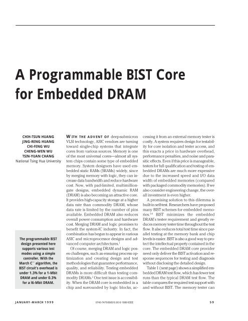
A <strong>Programmable</strong> <strong>BIST</strong> <strong>Core</strong><br />
<strong>for</strong> <strong>Embedded</strong> <strong>DRAM</strong><br />
CHIH-TSUN HUANG<br />
JING-RENG HUANG<br />
CHI-FENG WU<br />
CHENG-WEN WU<br />
TSIN-YUAN CHANG<br />
National Tsing Hua University<br />
The programmable <strong>BIST</strong><br />
design presented here<br />
supports various test<br />
modes using a simple<br />
controller. With the<br />
March C − algorithm, the<br />
<strong>BIST</strong> circuit’s overhead is<br />
under 1.3% <strong>for</strong> a 1-Mbit<br />
<strong>DRAM</strong> and under 0.3%<br />
<strong>for</strong> a l6-Mbit <strong>DRAM</strong>.<br />
WITH THE ADVENT OF deep-submicron<br />
VLSI technology, ASIC vendors are turning<br />
toward single-chip systems that integrate<br />
cores from various sources. Memory is one<br />
of the most universal cores—almost all system<br />
chips contain some type of embedded<br />
memory. System designers have used embedded<br />
static RAMs (SRAMs) widely, since<br />
by merging memory with logic, they can increase<br />
data bandwidth and reduce hardware<br />
cost. Now, with pad-limited, multimilliongate<br />
designs, embedded dynamic RAM<br />
(<strong>DRAM</strong>) is also becoming an attractive core.<br />
It provides high-capacity storage at a higher<br />
data rate than commodity <strong>DRAM</strong>, whose<br />
data rate is limited by the number of pins<br />
available. <strong>Embedded</strong> <strong>DRAM</strong> also reduces<br />
overall power consumption and hardware<br />
cost. Merging <strong>DRAM</strong> and logic promises to<br />
benefit the system-IC industry. In fact, the<br />
combination has begun to appear in various<br />
ASIC and microprocessor designs and advanced<br />
computer architectures. 1<br />
Of course, merging <strong>DRAM</strong> and logic poses<br />
challenges, such as ensuring process optimization<br />
and creating design and test<br />
methodologies that guarantee per<strong>for</strong>mance,<br />
quality, and reliability. Testing embedded<br />
<strong>DRAM</strong>s is more difficult than testing commodity<br />
<strong>DRAM</strong>s. 2 One test issue is accessibility.<br />
When the <strong>DRAM</strong> core is embedded in a<br />
chip and surrounded by logic blocks, accessing<br />
it from an external memory tester is<br />
costly. A system requires design <strong>for</strong> testability<br />
<strong>for</strong> core isolation and tester access, and<br />
this exacts a price in hardware overhead,<br />
per<strong>for</strong>mance penalties, and noise and parasitic<br />
effects. Even if this price is manageable,<br />
testers <strong>for</strong> full qualification and testing of embedded<br />
<strong>DRAM</strong>s are much more expensive<br />
due to the increased speed and I/O data<br />
width of embedded memories (compared<br />
with packaged commodity memories). If we<br />
also consider engineering change, the overall<br />
investment is even higher.<br />
A promising solution to this dilemma is<br />
built-in self-test. Researchers have proposed<br />
many <strong>BIST</strong> schemes <strong>for</strong> embedded memories.<br />
3-8 <strong>BIST</strong> minimizes the embedded<br />
<strong>DRAM</strong>’s tester requirement and greatly reduces<br />
memory tester time throughout the test<br />
flow. It also reduces total test time since parallel<br />
testing at the memory bank and chip<br />
levels is easier. <strong>BIST</strong> is also a good way to protect<br />
the intellectual property contained in the<br />
core. The embedded <strong>DRAM</strong> core provider<br />
need only deliver the <strong>BIST</strong> activation and response<br />
sequences <strong>for</strong> testing and diagnosis<br />
without disclosing the detailed design.<br />
Table 1 (next page) shows a simplified embedded<br />
<strong>DRAM</strong> test flow, which has fewer test<br />
runs than the typical <strong>DRAM</strong> test flow. The<br />
table compares the required test support with<br />
and without <strong>BIST</strong>. The memory tester can<br />
JANUARY–MARCH 1999 0740-7475/99/$10.00 © 1999 IEEE 59
.<br />
<strong>BIST</strong> CORE<br />
Table 1. <strong>Embedded</strong> <strong>DRAM</strong> test runs and required test support<br />
with and without <strong>BIST</strong>.<br />
per<strong>for</strong>m functional test, dc/ac parametric test, and redundancy<br />
analysis (<strong>for</strong> laser repair). A typical <strong>BIST</strong> design supports<br />
only functional test, but partial support of parametric<br />
test, redundancy analysis, and even self-repair is possible<br />
with increased logic overhead. As the table indicates, <strong>BIST</strong><br />
can include the entire pre-burn-in test. <strong>BIST</strong> also simplifies<br />
the implementation of a burn-in board (which generates<br />
burn-in test patterns). Final test requires a memory tester only<br />
<strong>for</strong> speed sorting, and <strong>BIST</strong> can handle functional test. Since<br />
memory testers are very expensive, the reduction of tester<br />
time justifies the use of <strong>BIST</strong>.<br />
Here, we present a <strong>BIST</strong> design and implementation <strong>for</strong><br />
embedded <strong>DRAM</strong>. It supports built-in self-diagnosis by feeding<br />
error in<strong>for</strong>mation to the external tester. Moreover, using<br />
a specific test sequence, it can test <strong>for</strong> critical timing faults,<br />
reducing tester time <strong>for</strong> ac parametric test. The design supports<br />
wafer test, pre-burn-in test, burn-in, and final test. It is<br />
field-programmable; the user can program test algorithms<br />
using predetermined test elements (such as march elements,<br />
surround test elements, and refresh modes). The user can<br />
optimize the hardware <strong>for</strong> a specific embedded <strong>DRAM</strong> with<br />
a set of predetermined test elements. Our design is different<br />
from the microprogram-controlled <strong>BIST</strong> described in<br />
Dreibelbis et al., 8 which has greater flexibility but higher<br />
overhead. Because our design begins at the register-transferlanguage<br />
level, test element insertion (<strong>for</strong> higher test coverage)<br />
and deletion (<strong>for</strong> lower hardware overhead) are<br />
relatively easy.<br />
Fault models<br />
We consider faults that may occur in the <strong>DRAM</strong> core’s address<br />
decoder, read/write circuitry, and memory cell array.<br />
We categorize address decoder faults (AFs) according to<br />
their functional behavior: 9,10<br />
■<br />
■<br />
■<br />
■<br />
Test run Isolation only Isolation and <strong>BIST</strong><br />
Wafer probe Tester Tester/<strong>BIST</strong><br />
Pre-burn-in test Tester <strong>BIST</strong><br />
Burn-in Burn-in board <strong>BIST</strong><br />
Final test Tester Tester/<strong>BIST</strong><br />
A certain address cannot access any cell.<br />
A certain address accesses multiple cells simultaneously.<br />
No address can access a certain cell.<br />
Multiple addresses can access a certain cell.<br />
Typical faults of the read/write circuitry (including buses,<br />
sense amplifiers, and write buffers) are equivalent to<br />
faults in the memory cell array. For memory cell array faults,<br />
we follow the notation used in van de Goor: 10<br />
■ ↑ —a rising cell transition (due to a write operation)<br />
■ ↓ —a falling cell transition<br />
■ b —either a rising or a falling cell transition<br />
■ ∀ —any operation at a cell<br />
■ —a fault in a cell, where S is the value or operation<br />
activating the fault, F is the cell’s faulty value, S ∈<br />
{0, 1, ↑, ↓, b}, and F ∈ {0, 1}<br />
■ —a fault involving m cells, where S 1 ,<br />
… , S m− 1 are the conditions of the first m−1 cells required<br />
to activate the fault in cell m, F is the faulty value of cell<br />
m, and <strong>for</strong> all 1 ≤ i ≤ m, S i ∈ {0, 1, ↑, ↓, b}<br />
■<br />
■<br />
■<br />
■<br />
■<br />
The following are typical faults in the memory cell array: 9,10<br />
Stuck-at fault (SAF)—a cell or line sticks at 1 or 0; <br />
denotes a stuck-at-1 fault and a stuck-at-0 fault.<br />
Stuck-open fault (SOF)—a cell is not accessible due to,<br />
<strong>for</strong> example, a broken line or a permanent open switch.<br />
Transition fault (TF)—a cell fails to make a transition; it<br />
can be or .<br />
Data retention fault (DRF)—a cell fails to retain its logic<br />
value after a prespecified period of time.<br />
Coupling faults:<br />
Inversion (CFin)—a transition in one cell inverts the<br />
content of another; that is, or .<br />
Idempotent (CFid)—a transition in one cell <strong>for</strong>ces a constant<br />
value (1 or 0) into another; that is, , , , or .<br />
State (CFst)—a coupled cell or line is <strong>for</strong>ced to a certain<br />
value only if the coupling cell or line is in a given<br />
state; that is, , , , or .<br />
The preceding single-cell fault models also apply to wordoriented<br />
memories. Coupling faults between cells in different<br />
words behave the same as in a bit-oriented memory. But<br />
coupling between cells inside the same word will virtually<br />
disappear if the write operation can override the coupling<br />
effect; that is, the write operation can correct the fault. In<br />
that case, the coupling fault can be detected only when its<br />
effect is stronger than the write operation. For example, say<br />
that a 4-bit word b 3 b 2 b 1 b 0 has a CFst , where b 3 couples<br />
b 2 . Then writing 0101 to b 3 b 2 b 1 b 0 results in a faulty value of<br />
0001 when CFst is stronger than the write operation; otherwise,<br />
the fault effect is masked.<br />
Test algorithms<br />
Our <strong>BIST</strong> scheme’s default test algorithms are the march al-<br />
60 IEEE DESIGN & TEST OF COMPUTERS
.<br />
gorithms. Table 2 shows a bitoriented<br />
March C − algorithm<br />
as an example. 10 M 0 , …, M 5<br />
denote the six march elements.<br />
In each march element,<br />
we first specify the<br />
address sequence: ⇑ means<br />
the address sequence is in ascending<br />
order, ⇓ means the<br />
address changes in descending<br />
order, and c<br />
means either ⇑ or ⇓ is acceptable.<br />
Consider M 1 , <strong>for</strong> example;<br />
the address sequence<br />
begins at the lowest address<br />
and changes in ascending order<br />
toward the highest. For<br />
each address (memory cell),<br />
the algorithm per<strong>for</strong>ms a<br />
read operation (with an expected<br />
0 in the fault-free<br />
case), writes back the complemented<br />
bit immediately,<br />
and then continues to the<br />
next address. The algorithm<br />
is also called the March 10N<br />
algorithm because it requires<br />
10N read/write operations,<br />
where N is the number of<br />
memory cells (address locations).<br />
The March C − completely<br />
detects SAFs, unlinked AFs,<br />
unlinked TFs, and CFs (including<br />
CFins, CFids, and<br />
CFsts). 10 It also detects SOFs<br />
if we extend M 1 to R0W1R1,<br />
or M 2 to R1W0R0. The resulting<br />
algorithm is called the<br />
Table 2. March C⎺ algorithm (R: read; W: write).<br />
extended March C − algorithm. Since our embedded <strong>DRAM</strong><br />
is word-oriented, we modify the 10N algorithm as ⇑(Wa);<br />
⇑(RaWa′); ⇑(Ra′Wa); ⇓(RaWa′); ⇓( Ra′Wa); ⇑(Ra), where a<br />
represents a data word (the background word) and a′ is its<br />
complement. This word-oriented algorithm reduces to the<br />
bit-oriented algorithm when a is a single bit.<br />
We select background words on the basis of the defined<br />
fault models and required fault coverage. Exhaustive data<br />
backgrounds are usually unaf<strong>for</strong>dable and unnecessary.<br />
Although the word-oriented March C − algorithm detects all<br />
the SAFs, unlinked AFs, TFs, and SOFs, coupling faults in the<br />
same word may not be detectable. The choice of data backgrounds<br />
determines the coverage of this kind of fault.<br />
March element M 0 M 1 M 2 M 3 M 4 M 5<br />
Address sequence c(W 0); ⇑(R0W 1); ⇑(R1W 0); ⇓(R 0W1); ⇓(R1W 0); c(R 0)<br />
Table 3. Three algorithms’ fault coverage (%): MATS++ (a); March X (b); March C⎺ (c).<br />
Fault P 1 P 2 P 3 P 2,3 P 1,2,3 P all<br />
SAF 100.0 100.0 100.0 100.0 100.0 100.0<br />
SOF 100.0 100.0 100.0 100.0 100.0 100.0<br />
TF 100.0 100.0 100.0 100.0 100.0 100.0<br />
AF 99.7 99.9 99.9 100.0 100.0 100.0<br />
CFin 100.0 100.0 100.0 100.0 100.0 100.0<br />
CFid 37.5 37.5 37.5 62.6 75.9 89.1<br />
CFst 50.0 50.0 50.0 75.0 87.5 100.0<br />
(a)<br />
SAF 100.0 100.0 100.0 100.0 100.0 100.0<br />
SOF 0.8 0.8 0.8 0.8 0.8 0.8<br />
TF 100.0 100.0 100.0 100.0 100.0 100.0<br />
AF 99.7 99.9 99.9 100.0 100.0 100.0<br />
CFin 100.0 100.0 100.0 100.0 100.0 100.0<br />
CFid 50.0 50.0 50.0 78.1 90.7 100.0<br />
CFst 62.5 62.5 62.5 84.4 93.0 100.0<br />
(b)<br />
SAF 100.0 100.0 100.0 100.0 100.0 100.0<br />
SOF 0.8 0.8 0.8 0.8 0.8 0.8<br />
TF 100.0 100.0 100.0 100.0 100.0 100.0<br />
AF 99.7 99.9 99.9 100.0 100.0 100.0<br />
CFin 100.0 100.0 100.0 100.0 100.0 100.0<br />
CFid 99.9 99.9 99.9 99.95 100.0 100.0<br />
CFst 99.9 99.9 99.9 99.95 100.0 100.0<br />
(c)<br />
Fault coverage evaluation<br />
We know a march algorithm’s coverage of its target faults<br />
by definition. However, to know its coverage of other faults<br />
requires further analysis. For example, the March X algorithm<br />
was designed to test all AFs, SAFs, TFs, and CFins, so<br />
its coverage of these faults is 100%. But to determine its coverage<br />
of CFids and CFsts, we must per<strong>for</strong>m analysis.<br />
Moreover, <strong>for</strong> a word-oriented memory such as we are discussing<br />
here, fault coverage also depends on the selected<br />
data backgrounds. Since there are so many possible faults<br />
and test algorithms (including address sequences,<br />
read/write operations, and data patterns/backgrounds), determining<br />
the algorithm that best balances cost and test cov-<br />
JANUARY–MARCH 1999 61
.<br />
<strong>BIST</strong> CORE<br />
Memory <strong>BIST</strong><br />
Q<br />
D<br />
18-bit<br />
address<br />
xRAS<br />
xCAS<br />
xWE<br />
Column address<br />
buffers<br />
Row address<br />
buffers<br />
Refresh<br />
controller<br />
Timing<br />
controller<br />
erage is difficult.<br />
We group faults into two classes: single-cell faults and faults<br />
involving two cells (such as coupling faults). We can test <strong>for</strong><br />
single-cell faults such as SAFs with an algorithm using any<br />
single data background because it tests all cells in the same<br />
way as <strong>for</strong> a bit-oriented memory. Two-cell faults, however,<br />
depend on the strength of the write operation and the coupling<br />
effect. Suppose the write operation erases the coupling<br />
effect between two cells in the same word. Such faults are<br />
redundant, and we must consider only coupling between<br />
two different words, so one background is sufficient.<br />
However, if the coupling effect is stronger than the write operation,<br />
we must consider coupling faults inside a word. This<br />
is the assumption in the following analysis.<br />
We can derive fault coverage by manual analysis, but that<br />
is tedious and sometimes impractical <strong>for</strong> complex test algorithms<br />
and fault models. Instead, we implemented a memory<br />
fault simulator called RAMSES (RAM Simulator <strong>for</strong> Error<br />
Screening) <strong>for</strong> this purpose. For a word-oriented memory<br />
with 4-bit words, the data backgrounds (patterns) commonly<br />
used are 0000 (P 1 ), 0101 (P 2 ), and 0011 (P 3 ). To make the list<br />
complete, we also consider 0110 (P 4 ), 0001 (P 5 ), 0010 (P 6 ),<br />
0100 (P 7 ), and 1000 (P 8 ). We simulated several test algorithms<br />
with RAMSES, assuming a 1-Kbyte word-oriented embedded<br />
<strong>DRAM</strong> with 4-bit words. Table 3 shows the fault<br />
coverage simulation results <strong>for</strong> the algorithms, in which P 2,3<br />
stands <strong>for</strong> {P 2 , P 3 }, P 1,2.3 <strong>for</strong> {P 1 , P 2 , P 3 }, and P all <strong>for</strong> {P 1 , P 2 , …,<br />
P 8 }. We show only the results <strong>for</strong> some data backgrounds,<br />
16<br />
16<br />
8<br />
10<br />
Row decoder<br />
1024<br />
Figure 1. <strong>Embedded</strong> EDO <strong>DRAM</strong> connected to <strong>BIST</strong> circuitry.<br />
Data out registers<br />
Data in registers<br />
Column decoder<br />
256<br />
Sense amplifiers<br />
1-Mbit<br />
memory<br />
array<br />
16<br />
16<br />
4-Mbit embedded<br />
EDO <strong>DRAM</strong><br />
although we per<strong>for</strong>med extensive<br />
simulations. We<br />
found that, in general, P 2<br />
provides the highest fault<br />
coverage among single<br />
backgrounds, and P 2,3 is the<br />
best among double backgrounds.<br />
For triple backgrounds,<br />
P 1,2,3 provides the<br />
highest fault coverage.<br />
Intuitively, uni<strong>for</strong>mity is not<br />
desirable so far as testing is<br />
concerned.<br />
For <strong>DRAM</strong>s, we may have<br />
to consider additional faults,<br />
such as neighborhood-pattern-sensitive<br />
and linked<br />
faults. If such faults are to be<br />
targeted after failure analysis,<br />
we need simulation to select<br />
the best test algorithms<br />
<strong>for</strong> them.<br />
The simulation results<br />
show that using multiple data<br />
backgrounds significantly increases the coverage of coupling<br />
faults <strong>for</strong> MATS++ 10 and March X compared with using a single<br />
background. However, <strong>for</strong> March C − , the improvement is<br />
minor—with only a background P 1 , the algorithm covers most<br />
of the faults. (The SOF fault coverage in Table 3c will reach<br />
100% if M 1 is extended to RaWa′Ra′.) Using an additional<br />
background doubles the test time but detects only a small<br />
percentage of additional faults (intraword coupling faults).<br />
Also, <strong>for</strong> larger <strong>DRAM</strong>s (with the same word length), the fault<br />
coverage of March C − does not decrease; rather, it increases<br />
since the percentage of undetected faults decreases.<br />
<strong>DRAM</strong> specification and <strong>BIST</strong> design strategy<br />
Since extended data-out (EDO) <strong>DRAM</strong>s are common, we<br />
use a 1-Mbit × 4 EDO <strong>DRAM</strong> as our example <strong>for</strong> explaining<br />
the proposed <strong>BIST</strong> design. Of course, one can easily apply<br />
the scheme to other embedded <strong>DRAM</strong> architectures. Our<br />
design assumes the embedded <strong>DRAM</strong> has four memory<br />
banks, each organized as a 1-Mbit array; thus, it has 256K addressable<br />
locations, each containing four bits. Figure 1<br />
shows a block diagram of the embedded <strong>DRAM</strong> with the<br />
proposed <strong>BIST</strong> scheme (detailed later). The timing controller<br />
controls the address buffers, data I/O buffers, and refresh<br />
mechanism via signals xRAS, xCAS, and xWE, which<br />
represent row address strobe, column address strobe, and<br />
write enable. <strong>Embedded</strong> <strong>DRAM</strong>s normally use separate I/O<br />
channels instead of multiplexed pins as in commodity<br />
<strong>DRAM</strong>s, so row and column addresses and data input (D)<br />
62 IEEE DESIGN & TEST OF COMPUTERS
.<br />
and output (Q) channels are<br />
all separate.<br />
One of the challenges of<br />
memory <strong>BIST</strong> is that the<br />
asynchronous memory core<br />
(traditional RAMs are asynchronous)<br />
must be tested by<br />
the synchronous <strong>BIST</strong> logic.<br />
This is especially difficult in<br />
embedded <strong>DRAM</strong>s. To illustrate<br />
how we cope with this<br />
problem, we use typical<br />
EDO <strong>DRAM</strong> timing specifications.<br />
The proposed strategy<br />
is not limited to the<br />
given EDO <strong>DRAM</strong> architecture.<br />
Figure 2 shows the<br />
typical EDO page-mode<br />
read-write cycle. Although in<br />
this case D and Q share the<br />
same I/O channel, our strategy<br />
still works (timing control<br />
of separate I/O channels<br />
is in fact easier). Table 4 lists<br />
the values of the timing parameters<br />
shown in Figure 2.<br />
The EDO page mode’s timing<br />
depends mainly on the<br />
edges of the four signals<br />
xRAS, xCAS, xWE, and xOE.<br />
They determine the time to<br />
latch the row address, column<br />
address, and input data<br />
<strong>for</strong> the memory core, as well<br />
as the output data <strong>for</strong> use by<br />
other cores.<br />
For embedded <strong>DRAM</strong>,<br />
which has no pin count limitation,<br />
D and Q can be separate<br />
to simplify control;<br />
there<strong>for</strong>e, output enable signal<br />
xOE can be removed<br />
without affecting functionality.<br />
The <strong>BIST</strong> logic, however,<br />
still needs xOE to indicate the arrival of the output data.<br />
We must determine an appropriate <strong>BIST</strong> clock period<br />
based on the xCAS cycle time (period) of the EDO page<br />
mode, t CAS in Table 4. In our example, the minimum t CAS is<br />
10 ns, which we use as the basis of the test clock period. We<br />
can select a test clock of up to 100 MHz.<br />
Instead of a memory tester, we need only a simple logic<br />
tester, which is slower and less expensive, to activate the<br />
Table 4. Timing parameter values of EDO page-mode read-write cycle.<br />
Parameter Min (ns) Max (ns) Description<br />
t AA 25 Access time from column address<br />
t ASC 0 Column address setup time<br />
t ASR 0 Row address setup time<br />
t AWD 42 Column-address-to-xWE delay<br />
t CAC 13 Access time from xCAS<br />
t CAH 10 Column address hold time<br />
t CAS 10 10,000 xCAS active pulsewidth<br />
t CP 10 xCAS precharge pulsewidth<br />
t CWD 28 xCAS-to-xWE delay<br />
t DH 10 D hold time<br />
t DS 0 D setup time<br />
t OD 0 12 Output disable<br />
t OEA 12 Access time from xOE<br />
t RAC 50 Access time from xRAS<br />
t RASP 55 125,000 xRAS (EDO page-mode) pulsewidth<br />
t RCD 12 xRAS-to-xCAS delay<br />
t RAH 10 Row address hold time<br />
t RP 30 xRAS precharge pulsewidth<br />
t WP 5 Write pulsewidth<br />
xRAS<br />
xCAS<br />
Addr<br />
xWE<br />
DQ<br />
xOE<br />
t RP<br />
t RCD<br />
t RASP<br />
t CAS t CP<br />
t<br />
t ASC<br />
t RAH<br />
ASR t CAH<br />
Row Column Column Column<br />
t CWD t WP<br />
t AWD<br />
t AA<br />
t CAC<br />
t DS<br />
t RAC<br />
t OEA<br />
Q D Q D<br />
t OD<br />
Figure 2. Timing diagram of EDO page-mode read-write cycle.<br />
<strong>BIST</strong> logic and receive the test result. The <strong>BIST</strong> sequencer<br />
(a timing sequence generator) generates timing signals<br />
based on the clock period; that is, it converts a long or short<br />
timing signal duration to a certain number of clock periods.<br />
Once the signal is converted, it is fixed in the <strong>BIST</strong> design;<br />
there<strong>for</strong>e, we must determine the clock period with care to<br />
avoid violation of the embedded <strong>DRAM</strong>’s timing specifications.<br />
In our example, we assume the clock period (and the<br />
t DH<br />
Q<br />
D<br />
JANUARY–MARCH 1999 63
.<br />
<strong>BIST</strong> CORE<br />
xCAS period) to be 20 ns (though it can be reduced almost<br />
to 10 ns). Once the clock period is fixed, we determine the<br />
other two related timing parameters, xRAS and xWE, accordingly.<br />
Also, we shift and stretch the address, D, and Q signals<br />
in the original timing diagram (Figure 2) according to<br />
the following rules. Note that Table 4 specifies t RAC , <strong>for</strong> example,<br />
as no more than 50 ns. This means the embedded<br />
<strong>DRAM</strong> design guarantees that Q is available 50 ns after the<br />
falling transition of xRAS (see Figure 2); thus, the sampling<br />
of Q should take place at least 50 ns after xRAS.<br />
■<br />
■<br />
The row address must be ready be<strong>for</strong>e xRAS goes low,<br />
and the column address must be ready be<strong>for</strong>e xCAS<br />
goes low. The time the address is stable be<strong>for</strong>e the address<br />
strobe is usually more than one clock cycle, meeting<br />
our design’s 0-ns setup time requirement. Also, the<br />
address remains stable <strong>for</strong> more than one clock cycle,<br />
meeting the 10-ns hold time requirement.<br />
The timing requirement <strong>for</strong> input data D is the same as<br />
<strong>for</strong> the column address.<br />
■ The major parameters related to output data Q are t AA ,<br />
t RAC , and t CAC , which are 25 ns (max), 50 ns (max), and<br />
13 ns (max). The xCAS low period (t CAS ) should span at<br />
least two clock cycles, since Q will settle at the beginning<br />
of the second cycle, and the clock cycle (20 ns) is<br />
longer than 13 ns. Since the column address is ready<br />
one clock cycle be<strong>for</strong>e the transition of xCAS (see the<br />
first rule), we let the time from xCAS to Q be two clock<br />
cycles to satisfy the t RAC constraint. Finally, the first falling<br />
transition of xCAS in page mode is delayed <strong>for</strong> one more<br />
clock cycle, so there are at least three clock cycles from<br />
xRAS to Q, satisfying the t RAC specification.<br />
■<br />
For the write operation (as in the page-mode read-write<br />
cycle), the key parameters are t AWD and t CWD . Because Q<br />
is sampled at the second clock after xCAS goes low, one<br />
BCK<br />
xRAS<br />
xCAS<br />
ADDR 3ff 0ff 0fe 0fd<br />
xWE<br />
Data in<br />
Q out aaaa aaaa aaaa<br />
xOE<br />
Figure 3. A timing diagram generated by the sequencer.<br />
5555 5555 5555<br />
more clock cycle must be inserted into the low period<br />
of xCAS, making it at least three cycles.<br />
Following these rules, the sequencer can generate wave<strong>for</strong>ms<br />
of the critical timing parameters to meet the specification.<br />
Slight adjustments may be necessary <strong>for</strong> other timing<br />
parameters. Figure 3 shows the wave<strong>for</strong>m diagram of RaWa′<br />
generated by the sequencer according to the rules and plotted<br />
by a timing simulator. The sequencer can also generate<br />
wave<strong>for</strong>ms <strong>for</strong> other march elements and retention and refresh<br />
test elements according to similar rules.<br />
<strong>BIST</strong> architecture and function<br />
Figure 4 diagrams our <strong>BIST</strong> design and the interface between<br />
the <strong>BIST</strong> logic and the embedded <strong>DRAM</strong>. The <strong>BIST</strong> activation<br />
control (BAC) input activates the <strong>BIST</strong> logic; the<br />
embedded <strong>DRAM</strong> is in normal mode when BAC is 0 and in<br />
<strong>BIST</strong> mode when BAC is 1. The <strong>BIST</strong> controller is a finite-state<br />
machine; its state transition is controlled by the <strong>BIST</strong> control<br />
selection (BCS) input. The <strong>BIST</strong> controller also controls the<br />
scan chains, shifting in test patterns and commands from the<br />
<strong>BIST</strong> scan-in (BSI) input and shifting out results from the <strong>BIST</strong><br />
scan-out (BSO) output. As Figure 4 shows, the controller contains<br />
multiple chains. The decode logic and test mode selection<br />
modules determine the proper data register to scan in<br />
the test commands and subsequently activate the sequencer.<br />
The sequencer generates the <strong>DRAM</strong>’s timing sequence, with<br />
the help of some built-in counters and the timing generator.<br />
The comparator compares and reports any discrepancy between<br />
the output data from the <strong>DRAM</strong> and the original input<br />
data generated by the sequence controller.<br />
The <strong>BIST</strong> logic has three additional I/O signals. The <strong>BIST</strong><br />
ready flag (BRD*) indicates when the <strong>BIST</strong> sequence is finished,<br />
so that the go/no-go indicator signal (BGO) can be<br />
sampled to check that the embedded <strong>DRAM</strong> is functioning<br />
correctly. The ⎺B⎺R⎺S*/<br />
SCAN signal acts as both the<br />
reset and scan test control.<br />
All registers in the <strong>BIST</strong> controller<br />
finite-state machine<br />
are scanned, and be<strong>for</strong>e we<br />
use the <strong>BIST</strong> logic to test the<br />
<strong>DRAM</strong>, the logic itself is scan<br />
tested. Finally, we need a<br />
<strong>BIST</strong> clock (BCK) input.<br />
BCK and BAC must be<br />
dedicated; others cannot<br />
share these two input pins<br />
(<strong>for</strong> example, by using multiplexers).<br />
But BRD* is optional<br />
and may be removed<br />
if pin count is a concern. In<br />
64 IEEE DESIGN & TEST OF COMPUTERS
.<br />
BGO<br />
BRD*<br />
Sequencer<br />
xOB<br />
Data background<br />
composer<br />
Comparator<br />
Q<br />
D<br />
16<br />
16<br />
Row address counter<br />
Column address counter<br />
BSO<br />
Sequence<br />
controller<br />
Control<br />
counter<br />
Timing<br />
generator<br />
<strong>DRAM</strong> interface buffers<br />
18-bit<br />
address<br />
4-Mbit<br />
embedded<br />
EDO<br />
<strong>DRAM</strong><br />
<strong>BIST</strong> scan path<br />
Burn-in commands<br />
BSI<br />
March commands/data<br />
xRAS<br />
Diagnosis in<strong>for</strong>mation<br />
xCAS<br />
BCK<br />
Test mode selection<br />
xWE<br />
Decode logic<br />
BCS<br />
BAC<br />
BRS*/SCAN<br />
Controller<br />
<strong>BIST</strong> controller<br />
Memory <strong>BIST</strong><br />
Figure 4. Block diagram of the proposed <strong>BIST</strong> design connected to the embedded EDO <strong>DRAM</strong>.<br />
that case, we can encode BGO to signal the completion of<br />
the <strong>BIST</strong> sequence and show the test result. The reset<br />
(⎺B⎺R⎺S*) also is optional, since a short synchronizing sequence<br />
<strong>for</strong> the <strong>BIST</strong> controller can be the reset sequence.<br />
However, the SCAN pin is still required in that case. Apart<br />
from BCK and BAC, all other <strong>BIST</strong> I/O signals can share pins<br />
with signals outside the <strong>DRAM</strong> core; thus, we can use multiplexed<br />
pins to reduce pin overhead.<br />
The proposed <strong>BIST</strong> supports the following test modes:<br />
■<br />
Scan test—testing the <strong>BIST</strong> logic, except the <strong>BIST</strong> controller<br />
finite-state machine. We execute scan test at the<br />
beginning of the <strong>BIST</strong> sequence to ensure the circuit’s<br />
■<br />
■<br />
correct functionality. In addition, we test all registers in<br />
the <strong>DRAM</strong> core in this mode.<br />
Memory <strong>BIST</strong>—functional testing of the <strong>DRAM</strong> using<br />
march algorithms. This mode exercises various operation<br />
modes, such as non-page-mode test, page mode<br />
test, refresh test, and retention test. This mode also supports<br />
diagnosis. In that case, the <strong>BIST</strong> logic can shift out<br />
the address of any faulty cell, column, or row to the external<br />
tester via the scan mechanism. We can test <strong>for</strong> retention<br />
faults in this mode or in a separate test mode.<br />
Burn-in—stress testing to screen out unreliable parts that<br />
may fail in infancy. This mode uses the <strong>BIST</strong> logic to exercise<br />
the entire memory cell array in a more efficient<br />
JANUARY–MARCH 1999 65
.<br />
<strong>BIST</strong> CORE<br />
■<br />
0<br />
0<br />
0<br />
BCS = 0<br />
Initial<br />
1<br />
Test_mode_in<br />
0<br />
Decode<br />
1<br />
Data_in_out<br />
0<br />
Apply<br />
1<br />
Execute<br />
Exit<br />
0<br />
1<br />
Probe/pause<br />
Figure 5. <strong>BIST</strong> controller state diagram.<br />
0<br />
1<br />
1<br />
1<br />
1<br />
Initial/reset state: all <strong>BIST</strong> outputs<br />
retain safe values<br />
Test mode selection<br />
Command decoding<br />
Data scan: shift in test inputs and<br />
shift out results<br />
Scan test application and<br />
<strong>BIST</strong> activation<br />
Memory function test,<br />
BI, AC test, etc.<br />
Pause <strong>for</strong> observation, or exit the<br />
execution phase<br />
Shift out results,<br />
or pause <strong>for</strong> retention test<br />
method than the normal read/write access. The default<br />
burn-in test is to use a march algorithm supported in the<br />
memory <strong>BIST</strong> mode.<br />
Timing-fault test—testing <strong>for</strong> critical timing faults by running<br />
the <strong>BIST</strong> clock at an appropriate speed. Among<br />
these faults are incorrect setup time, hold time, and data<br />
arrival time of various control and data signals. We can<br />
simultaneously detect some timing faults, such as incorrect<br />
setup time and hold time, when we per<strong>for</strong>m<br />
functional test (in memory <strong>BIST</strong> mode). We can test <strong>for</strong><br />
others by using different <strong>BIST</strong> clock periods or an external<br />
memory tester.<br />
Our design can include other test modes if necessary,<br />
since the control scheme is flexible. Of course, <strong>for</strong> dc parameter<br />
test, we must still use an external tester’s parameter<br />
measurement unit.<br />
<strong>BIST</strong> implementation<br />
As shown in Figure 4, the <strong>BIST</strong> logic consists of two parts:<br />
controller and sequencer. The controller takes charge of the<br />
overall <strong>BIST</strong> flow, and the sequencer generates the embedded<br />
<strong>DRAM</strong>’s address, data, and timing sequences. At the<br />
ASIC level, logic <strong>BIST</strong> and memory <strong>BIST</strong> can share the same<br />
controller, and the on-chip processor can function as the sequencer<br />
during memory <strong>BIST</strong> mode. However, <strong>for</strong> a <strong>DRAM</strong><br />
core delivered as intellectual property to be embedded in<br />
various chips, we must integrate a complete <strong>BIST</strong> circuit with<br />
the <strong>DRAM</strong> core. We consider the latter case.<br />
Controller. After the scan test mode has finished successfully,<br />
we enter the memory <strong>BIST</strong> mode. The <strong>BIST</strong> controller<br />
finite-state machine controls the scan test and <strong>BIST</strong><br />
flow to test the rest of the <strong>BIST</strong> circuitry and the embedded<br />
<strong>DRAM</strong>. Figure 5 shows the state diagram of the proposed finite-state<br />
machine. Each arc in the figure represents a state<br />
transition controlled by BCS. We enter the initial state by asserting<br />
⎺B⎺R⎺S*/SCAN low or applying a synchronizing sequence.<br />
By applying four continuous 0’s on BCS, we can<br />
return to the initial state from any other state.<br />
From the initial state, we enter the test_mode_in state if<br />
BCS is 1. In this state, we select the intended test mode. The<br />
decode state generates all internal control signals, including<br />
those <strong>for</strong> the selection of the proper scan chain <strong>for</strong> the<br />
data sequence to be shifted in. User-specified parameters<br />
and the test algorithm are shifted in during the data_in_out<br />
state. Note that the decode, data_in_out, and apply states<br />
<strong>for</strong>m a loop <strong>for</strong> running the scan test. We per<strong>for</strong>m other test<br />
modes in the execute state. For memory core testing and diagnosis,<br />
we enter the bottom loop, which contains the execute,<br />
exit, and probe/pause states, and collect the error<br />
in<strong>for</strong>mation in the probe/pause state. We can also run retention<br />
test in the probe/pause state, which allows pausing<br />
<strong>for</strong> a user-determined interval.<br />
An alternative approach is to add an extra mode in the sequencer,<br />
using a counter <strong>for</strong> measuring the time interval from,<br />
<strong>for</strong> example, xCAS to xWE. We can derive appropriate timing<br />
sequences using similar rules as <strong>for</strong> march tests. When diagnosis<br />
is required, the sequencer tests the entire memory core;<br />
in other words, the process does not stop immediately when<br />
an error is detected. It is not necessary to continue the testing<br />
process when an error is found if we per<strong>for</strong>m testing but not<br />
diagnosis. The sequencer will simply halt and indicate that<br />
an error is found, and the controller can go back to the decode<br />
state through the exit state. From there, either we can<br />
reach the initial state, or we can reenter the data_in_out state<br />
again. The apply, execute, exit, and probe/pause states can be<br />
merged if diagnosis is not required.<br />
Figure 6 shows the <strong>BIST</strong> circuit’s timing diagram (the entire<br />
control sequence). As discussed earlier, when BAC is 1,<br />
66 IEEE DESIGN & TEST OF COMPUTERS
.<br />
the <strong>DRAM</strong> enters the memory<br />
<strong>BIST</strong> mode, in which every<br />
BCK<br />
signal is synchronized to BAC Normal mode <strong>BIST</strong> mode<br />
<strong>BIST</strong> clock BCK. As depicted<br />
in the figure,⎺B⎺R⎺S*/SCAN is BRS*/SCAN<br />
Controller test<br />
pulled high at the beginning<br />
of the memory <strong>BIST</strong> mode to BCS<br />
Scan test control<br />
per<strong>for</strong>m the scan test verifying<br />
the <strong>BIST</strong> controller’s correctness.<br />
A scan chain <strong>for</strong>ms<br />
BRD*<br />
between BSI and BSO <strong>for</strong> applying<br />
patterns and collect-<br />
BGO<br />
BSI<br />
Test patterns<br />
ing responses in this phase.<br />
After the scan,⎺B⎺R⎺S*/SCAN is<br />
BSO<br />
Test outputs<br />
pulled low to reset the <strong>BIST</strong><br />
controller (BCS remains low Figure 6. <strong>BIST</strong> circuit control sequence.<br />
to generate the reset sequence<br />
if necessary). The<br />
<strong>BIST</strong> controller then per<strong>for</strong>ms a scan test <strong>for</strong> the rest of the<br />
<strong>BIST</strong> circuit. The test algorithm is subsequently applied according<br />
to the control flow discussed earlier and the finitestate<br />
machine shown in Figure 5. Finally, after BRD* is<br />
asserted high and BGO is sampled, we let BAC equal 0 to return<br />
the <strong>DRAM</strong> to normal mode.<br />
In the controller, we implemented several default<br />
read/write commands, address orders, data backgrounds,<br />
and EDO <strong>DRAM</strong> access modes. The built-in read/write commands<br />
are Ra (read the expected word a), Wa (write word<br />
a), RaWa′ (read word a, complement, and then write back<br />
immediately), and RaWa′Ra′. The default address orders include<br />
⇑ and ⇓, implemented by an up-down counter. The<br />
built-in access modes to be used in conjunction with the address<br />
orders are row scan, column scan, page-mode column<br />
scan, and refresh. The data background word (a) is supplied<br />
online. Each march element is a combination of the appropriate<br />
read/write command, address order, access mode,<br />
and data background.<br />
In addition to the march commands, our <strong>BIST</strong> also supports<br />
diagnosis, burn-in, and retention test. Other test commands<br />
can be integrated easily. In our scheme, a test<br />
algorithm is a sequence of commands entered from the BSI<br />
pin to the scan chains, decoded, and executed (see Figure<br />
4). When the controller encounters a special end-ofalgorithm<br />
command, it detects the end of a test algorithm.<br />
In our default implementation, most march algorithms can<br />
be programmed, including the extended March C − , March<br />
X, March Y, MATS++, and others.<br />
Sequencer. In designing the sequencer, our major goal was<br />
flexibility. Our sequencer design can be used <strong>for</strong> a wide range of<br />
<strong>DRAM</strong> cores with various operation modes, memory dimensions,<br />
and timing specifications. Figure 7 (next page) shows the state<br />
Reset<br />
sequence<br />
Scan test<br />
Scan in<br />
Scan out<br />
Commands/data<br />
<strong>BIST</strong> control sequence<br />
Go/No-Go<br />
Observe<br />
diagram of the sequence controller finite-state machine (see<br />
Figure 4). As the state diagram shows, we implemented timing<br />
sequence generation modules <strong>for</strong> the single read/write commands<br />
and the page-mode read/write commands <strong>for</strong> the march<br />
elements defined in the controller. We also implemented a refresh<br />
timing generation module <strong>for</strong> refresh tests. The figure shows<br />
the sequence controller’s default implementation, which is designed<br />
<strong>for</strong> march tests, but we can easily extend it to other algorithms.<br />
An important concern is that the sequencer’s outputs be<br />
glitch-free, and that they be in high impedance when <strong>BIST</strong> is not<br />
in use—that is, in normal operation mode. Our implementation<br />
takes these requirements into consideration. In Figure 7, the state<br />
transition is on BCK’s rising edge, while the control (timing) signals<br />
<strong>for</strong> the <strong>DRAM</strong> core are applied on BCK’s falling edge.<br />
Consequently, the sequencer’s outputs are guaranteed glitch-free.<br />
When the embedded <strong>DRAM</strong> is in normal mode, the sequence<br />
controller is in the idle state, where it stays until the<br />
<strong>BIST</strong> controller enters the execute state. Then the sequence<br />
controller fetches the march commands, enters the reset<br />
state, and carries out the sequence <strong>for</strong> the specified memory<br />
access mode. For memory access modes such as Ra, Wa,<br />
RaWa′, and RaWa′Ra′, the timing wave<strong>for</strong>m is periodic, and<br />
the period depends on the row access cycle. We inserted<br />
appropriate refresh cycles <strong>for</strong> refresh timing. The page-mode<br />
access cycle consists of the row access and column access<br />
cycles. The <strong>DRAM</strong> core latches the row address first; then it<br />
latches the column addresses of the whole page one by one.<br />
In the self-refresh/hidden-refresh/RAS-only-refresh state, the<br />
embedded <strong>DRAM</strong> is tested <strong>for</strong> its refresh mechanism.<br />
As shown in Figure 4, the sequencer design is based on<br />
counters. If the memory size increases, only the lengths of<br />
the row address and column address counters and the size<br />
of the comparator increase. Only one additional bit is required<br />
<strong>for</strong> an address counter when memory size doubles, so<br />
JANUARY–MARCH 1999 67
.<br />
<strong>BIST</strong> CORE<br />
Reset<br />
Idle<br />
Refresh<br />
Ra<br />
Wa<br />
RaWa′<br />
RaWa′Ra′<br />
Page-mode<br />
row<br />
Page-mode<br />
column Ra<br />
Page-mode<br />
row<br />
Page-mode<br />
column Wa<br />
Page-mode<br />
row<br />
Page-mode<br />
column<br />
RaWa′<br />
Page-mode<br />
row<br />
Page-mode<br />
column<br />
RaWa′Ra′<br />
Selfrefresh/<br />
hidden<br />
refresh/<br />
RASonly<br />
refresh<br />
Done<br />
Figure 7. State diagram of the sequence controller <strong>for</strong> march tests.<br />
Table 5. Comparison of embedded-<strong>DRAM</strong> test application methodologies.<br />
Test method Test time Hardware cost Coverage<br />
Ours Short Low Functional, timing, burn-in<br />
Processor-based Short Low Functional<br />
Scan Long Low Functional<br />
Tester Short Very high Functional, timing, dc<br />
hardware overhead is low. The control counter, designed to<br />
meet the refresh time specification, is used <strong>for</strong> retention/refresh<br />
test. Refresh time specifications <strong>for</strong> various <strong>DRAM</strong>s currently<br />
in use do not differ much regardless of size, so the<br />
sequencer’s area overhead actually drops when the <strong>DRAM</strong><br />
core’s size increases. In our example, a 21-bit counter suffices<br />
if the refresh cycle does not exceed 32 ms. The size of<br />
the entire <strong>BIST</strong> logic <strong>for</strong> the EDO <strong>DRAM</strong> core, without burnin<br />
and redundancy analysis, is about 2,000 to 3,000 gates.<br />
Following a command decoded by the controller, the sequencer<br />
generates the <strong>DRAM</strong> core’s required output signals,<br />
using a small look-up table (LUT). The LUT-based design reduces<br />
design ef<strong>for</strong>t and hardware cost by allowing new test<br />
commands to be added easily. When the timing specifications<br />
change, a simple program generates the LUT content<br />
automatically. The LUT-based design is an important step<br />
toward a <strong>BIST</strong> compiler <strong>for</strong> embedded <strong>DRAM</strong>s. It is configurable<br />
at the register-transfer-language level but does not<br />
modify the architecture. For non-march algorithms such as<br />
pseudorandom and surround test, one must design specific<br />
address counters or counter configurations <strong>for</strong> the sequencer<br />
and add new commands to the state diagram.<br />
Discussion<br />
We used a commercial synthesis tool and a single-poly,<br />
triple-metal logic cell library to estimate our <strong>BIST</strong> circuit’s area.<br />
Figure 8 plots <strong>BIST</strong> area overhead with respect to various<br />
<strong>DRAM</strong> core sizes. The <strong>DRAM</strong> areas are based on areas of existing<br />
0.25-µm and 0.35-µm EDO <strong>DRAM</strong> chips reported by major<br />
vendors. Comparisons are based on the areas estimated<br />
by the synthesis tool, so they are not exact. Also, it is impossible<br />
(and unnecessary) <strong>for</strong> us to project the precise size of<br />
our <strong>BIST</strong> circuit on all these <strong>DRAM</strong> chips. Since the overhead<br />
is very low, we expect the exact area overhead numbers to<br />
be close to those shown in the figure. Thus, the <strong>BIST</strong> area overhead<br />
<strong>for</strong> our default <strong>BIST</strong> design is about 1.3% <strong>for</strong> a 1-Mbit embedded<br />
<strong>DRAM</strong> and negligible <strong>for</strong> a 64-Mbit version. Even <strong>for</strong><br />
the 16-Mbit <strong>DRAM</strong>, the most popular embedded <strong>DRAM</strong> candidate<br />
currently, the <strong>BIST</strong> area overhead is less than 0.3%.<br />
Clearly, the larger the <strong>DRAM</strong> core, the smaller the <strong>BIST</strong> area<br />
overhead.<br />
Since the area overhead is<br />
low, one can include more<br />
test modes and algorithms to<br />
increase coverage, as long<br />
as test time does not become<br />
a problem. The test<br />
time <strong>for</strong> non-page-mode<br />
March C − , <strong>for</strong> example, is<br />
about 0.4 seconds <strong>for</strong> the 4-<br />
68 IEEE DESIGN & TEST OF COMPUTERS
.<br />
Memory area (µm 2 )<br />
140<br />
120<br />
100<br />
80<br />
60<br />
40<br />
20<br />
Memory area<br />
<strong>BIST</strong> overhead<br />
0 0<br />
1 4 16 64<br />
Memory size (Mbits)<br />
1.4<br />
1.2<br />
1<br />
0.8<br />
0.6<br />
0.4<br />
0.2<br />
<strong>BIST</strong> area overhead (%)<br />
makes designing and implementing appropriate <strong>BIST</strong> circuits<br />
<strong>for</strong> various embedded <strong>DRAM</strong>s systematic and easy.<br />
This <strong>BIST</strong> design has been implemented in an industry project<br />
in which we plan to evaluate its effectiveness in the future.<br />
Meanwhile, under demand from industry, we are working on<br />
an extended version that will incorporate built-in redundancy<br />
analysis and support more fault models.<br />
Acknowledgments<br />
Global UniChip Corporation (GUC), Hsinchu, Taiwan, under<br />
contract NTHU-0987-113J6, partly supported this work.<br />
Figure 8. Area overhead of the <strong>BIST</strong> core.<br />
Mbit core (assuming a 50-MHz clock). It increases approximately<br />
in proportion to the address space. To reduce test<br />
time, one can explore parallel testing of multiple banks or<br />
even multiple words by separate <strong>BIST</strong> sequencers, but that<br />
requires very careful modification of the memory core. Note<br />
that after dicing, an external memory tester is not needed<br />
until after burn-in—an important <strong>BIST</strong> benefit.<br />
Table 5 qualitatively summarizes some embedded <strong>DRAM</strong><br />
test application methods, including our <strong>BIST</strong> implementation,<br />
processor-based <strong>BIST</strong>, scan-based serial testing, 4 and direct<br />
memory tester access. Our method is very suitable <strong>for</strong> embedded<br />
<strong>DRAM</strong>, especially when the <strong>BIST</strong> circuitry is to be integrated<br />
with the <strong>DRAM</strong> core to <strong>for</strong>m a single piece of<br />
intellectual property <strong>for</strong> use in various ASICs. Moreover, by<br />
properly configuring the controller and sequencer, we can<br />
support timing-fault testing and burn-in. Processor-based <strong>BIST</strong><br />
is also popular in an ASIC environment, where an existing<br />
processor is available <strong>for</strong> the <strong>DRAM</strong> <strong>BIST</strong> designer. But it is<br />
not suitable <strong>for</strong> an embedded <strong>DRAM</strong> designed as a standalone,<br />
reusable intellectual property core. Serial <strong>BIST</strong> is not<br />
popular because it is slow. Also, the second and third methods<br />
normally support only functional test. The external memory<br />
tester is the most powerful but most expensive method. It<br />
supports all kinds of test (except burn-in) with very high resolution<br />
and programmability—and a very high cost.<br />
References<br />
1. D. Patterson et al., “A Case <strong>for</strong> Intelligent RAM,” IEEE Micro,<br />
Vol. 17, No. 2, Mar.-Apr. 1997, pp. 34-44.<br />
2. “A D&T Roundtable: Testing Mixed Logic and <strong>DRAM</strong> Chips,”<br />
IEEE Design & Test of Computers, Vol. 15, No. 2, Apr.-June 1998,<br />
pp. 86-92.<br />
3. R. Dekker, F. Beenker, and L. Thijssen, “A Realistic Self-Test<br />
Machine <strong>for</strong> Static Random Access Memories,” Proc. Int’l Test<br />
Conf., IEEE Computer Society Press, Los Alamitos, Calif., 1988,<br />
pp. 353-361.<br />
4. B. Nadeau-Dostie, A. Silburt, and V.K. Agarwal, “Serial Interface<br />
<strong>for</strong> <strong>Embedded</strong>-Memory Testing,” IEEE Design & Test of<br />
Computers, Vol. 7, No. 2, Apr. 1990, pp. 52-63.<br />
5. R. Treuer and V.K. Agarwal, “Built-In Self-Diagnosis <strong>for</strong> Repairable<br />
<strong>Embedded</strong> RAMs,” IEEE Design & Test of Computers,<br />
Vol. 10, No. 2, June 1993, pp. 24-33.<br />
6. P. Camurati et al., “Industrial <strong>BIST</strong> of <strong>Embedded</strong> RAMs,” IEEE<br />
Design & Test of Computers, Vol. 12, No. 3, Fall 1995, pp. 86-95.<br />
7. S. Tanoi et al., “On-Wafer <strong>BIST</strong> of a 200-Gb/s Failed-Bit Search<br />
<strong>for</strong> 1-Gb <strong>DRAM</strong>,” IEEE J. Solid-State Circuits, Vol. 32, No. 11, Nov.<br />
1997, pp. 1735-1742.<br />
8. J. Dreibelbis et al., “Processor-Based Built-In Self-Test <strong>for</strong> <strong>Embedded</strong><br />
<strong>DRAM</strong>,” IEEE J. Solid-State Circuits, Vol. 33, No. 11,<br />
Nov. 1998, pp. 1731-1740.<br />
9. R. Dekker, F. Beenker, and L. Thijssen, “Fault Modeling and<br />
Test Algorithm Development <strong>for</strong> Static Random Access Memories,”<br />
Proc. Int’l Test Conf., IEEE CS Press, 1988, pp. 343-352.<br />
10. A.J. van de Goor, “Using March Tests to Test SRAMs,” IEEE Design<br />
& Test of Computers, Vol. 10, No. 1, Mar. 1993, pp. 8-14.<br />
WE HAVE PROPOSED a flexible and cost-effective <strong>BIST</strong> design<br />
<strong>for</strong> embedded <strong>DRAM</strong>s. It supports march-based tests and<br />
diagnosis and timing specification tests. Our approach is flexible<br />
because additional test commands (other than march elements)<br />
can be included with little ef<strong>for</strong>t. It is cost-effective<br />
because test time is short, hardware overhead is low, and test<br />
coverage is high. It can also support burn-in if the <strong>DRAM</strong> core<br />
design is modified <strong>for</strong> that purpose. Together with the RAM-<br />
SES memory fault simulator, the proposed <strong>BIST</strong> approach<br />
Chih-Tsun Huang received the BSEE and<br />
MSEE degrees in electrical engineering from<br />
National Tsing Hua University, Hsinchu, Taiwan,<br />
where he is now working toward the<br />
PhD. His research areas include VLSI testing,<br />
embedded core and system design, design <strong>for</strong><br />
testability and reliability, and embedded<br />
memory testing. Huang is a student member of the IEEE.<br />
JANUARY–MARCH 1999 69
.<br />
<strong>BIST</strong> C<br />
Jing-Reng Huang received the BSEE and<br />
MSEE degrees in electrical engineering from<br />
National Tsing Hua University. He is currently<br />
working toward the PhD degree. His research<br />
interests are VLSI design, logic and<br />
memory built-in self-test, and computer arithmetic.<br />
Huang is a student member of the IEEE.<br />
Chi-Feng Wu received the BSEE and MSEE<br />
in electrical engineering from National Tsing<br />
Hua University and is currently working toward<br />
the PhD. His research interests are testing<br />
<strong>for</strong> programmable logic devices<br />
(including FPGAs and CPLDs), memory testing,<br />
and memory fault simulation. Wu is a student<br />
member of the IEEE.<br />
Cheng-Wen Wu is a professor in the Department<br />
of Electrical Engineering, National Tsing<br />
Hua University. He also has served as<br />
director of the university’s Computer and<br />
Communications Center and Technology Service<br />
Center. He was a guest editor of the Journal<br />
of In<strong>for</strong>mation Science and Engineering’s<br />
special issue on VLSI testing, and the technical program chair of the<br />
IEEE Fifth Asian Test Symposium. He received the 1996 NTHU<br />
Teaching Award and the 1997 Outstanding Electrical Engineering<br />
Professor Award from the Chinese Institute of Electrical Engineers<br />
(CIEE). Wu received the BSEE from National Taiwan University,<br />
Taipei, and the MS and PhD, both in electrical and computer engineering,<br />
from the University of Cali<strong>for</strong>nia, Santa Barbara. He is a<br />
member of CIEE and a senior member of IEEE.<br />
Tsin-Yuan Chang is an associate professor<br />
in the Department of Electrical Engineering,<br />
National Tsing Hua University. His research<br />
areas include VLSI design and testing, faulttolerant<br />
computing, and computer arithmetic.<br />
Chang received the BS from National Tsing<br />
Hua University and the MS and PhD from<br />
Michigan State University, all in electrical engineering. Chang is a<br />
member of the IEEE.<br />
Send questions and comments about this article to Cheng-Wen<br />
Wu, Dept. of Electrical Engineering, National Tsing Hua University,<br />
Hsinchu, Taiwan, ROC; cww@ee.nthu.edu.tw.<br />
70


