

Atmel AT89C52 Data Sheet
Atmel AT89C52 Data Sheet
Atmel AT89C52 Data Sheet

You also want an ePaper? Increase the reach of your titles
YUMPU automatically turns print PDFs into web optimized ePapers that Google loves.
Features<br />
• Compatible with MCS-51 Products<br />
• 8K Bytes of In-System Reprogrammable Flash Memory<br />
• Endurance: 1,000 Write/Erase Cycles<br />
• Fully Static Operation: 0 Hz to 24 MHz<br />
• Three-level Program Memory Lock<br />
• 256 x 8-bit Internal RAM<br />
• 32 Programmable I/O Lines<br />
• Three 16-bit Timer/Counters<br />
• Eight Interrupt Sources<br />
• Programmable Serial Channel<br />
• Low-power Idle and Power-down Modes<br />
Description<br />
The <strong>AT89C52</strong> is a low-power, high-performance CMOS 8-bit microcomputer with 8K<br />
bytes of Flash programmable and erasable read only memory (PEROM). The device<br />
is manufactured using <strong>Atmel</strong>’s high-density nonvolatile memory technology and is<br />
compatible with the industry-standard 80C51 and 80C52 instruction set and pinout.<br />
The on-chip Flash allows the program memory to be reprogrammed in-system or by a<br />
conventional nonvolatile memory programmer. By combining a versatile 8-bit CPU<br />
with Flash on a monolithic chip, the <strong>Atmel</strong> <strong>AT89C52</strong> is a powerful microcomputer<br />
which provides a highly-flexible and cost-effective solution to many embedded control<br />
applications.<br />
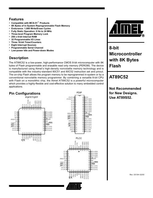
Pin Configurations<br />
PQFP/TQFP<br />
P1.5<br />
P1.6<br />
P1.7<br />
RST<br />
(RXD) P3.0<br />
NC<br />
(TXD) P3.1<br />
(INT0) P3.2<br />
(INT1) P3.3<br />
(T0) P3.4<br />
iT1) P3.5<br />
1<br />
2<br />
3<br />
4<br />
5<br />
6<br />
7<br />
8<br />
9<br />
10<br />
11<br />
P1.4<br />
P1.3<br />
P1.2<br />
P1.1 (T2 EX)<br />
P1.0 (T2)<br />
NC<br />
VCC<br />
P0.0 (AD0)<br />
P0.1 (AD1)<br />
P0.2 (AD2)<br />
P0.3 (AD3)<br />
44<br />
43<br />
42<br />
41<br />
40<br />
39<br />
38<br />
37<br />
36<br />
35<br />
34<br />
12<br />
13<br />
14<br />
15<br />
16<br />
17<br />
18<br />
19<br />
20<br />
21<br />
22<br />
33<br />
32<br />
31<br />
30<br />
29<br />
28<br />
27<br />
26<br />
25<br />
24<br />
23<br />
P0.4 (AD4)<br />
P0.5 (AD5)<br />
P0.6 (AD6)<br />
P0.7 (AD7)<br />
EA/VPP<br />
NC<br />
ALE/PROG<br />
PSEN<br />
P2.7 (A15)<br />
P2.6 (A14)<br />
P2.5 (A13)<br />
(T2) P1.0<br />
(T2 EX) P1.1<br />
P1.2<br />
P1.3<br />
P1.4<br />
P1.5<br />
P1.6<br />
P1.7<br />
RST<br />
(RXD) P3.0<br />
(TXD) P3.1<br />
(INT0) P3.2<br />
(INT1) P3.3<br />
(T0) P3.4<br />
(T1) P3.5<br />
(WR) P3.6<br />
(RD) P3.7<br />
XTAL2<br />
XTAL1<br />
GND<br />
1<br />
2<br />
3<br />
4<br />
5<br />
6<br />
7<br />
8<br />
9<br />
10<br />
11<br />
12<br />
13<br />
14<br />
15<br />
16<br />
17<br />
18<br />
19<br />
20<br />
PDIP<br />
40<br />
39<br />
38<br />
37<br />
36<br />
35<br />
34<br />
33<br />
32<br />
31<br />
30<br />
29<br />
28<br />
27<br />
26<br />
25<br />
24<br />
23<br />
22<br />
21<br />
VCC<br />
P0.0 (AD0)<br />
P0.1 (AD1)<br />
P0.2 (AD2)<br />
P0.3 (AD3)<br />
P0.4 (AD4)<br />
P0.5 (AD5)<br />
P0.6 (AD6)<br />
P0.7 (AD7)<br />
EA/VPP<br />
ALE/PROG<br />
PSEN<br />
P2.7 (A15)<br />
P2.6 (A14)<br />
P2.5 (A13)<br />
P2.4 (A12)<br />
P2.3 (A11)<br />
P2.2 (A10)<br />
P2.1 (A9)<br />
P2.0 (A8)<br />
8-bit<br />
Microcontroller<br />
with 8K Bytes<br />
Flash<br />
<strong>AT89C52</strong><br />
Not Recommended<br />
for New Designs.<br />
Use AT89S52.<br />
(WR) P3.6<br />
(RD) P3.7<br />
XTAL2<br />
XTAL1<br />
GND<br />
NC<br />
(A8) P2.0<br />
(A9) P2.1<br />
(A10) P2.2<br />
(A11) P2.3<br />
(A12) P2.4<br />
PLCC<br />
P1.4<br />
P1.3<br />
P1.2<br />
P1.1 (T2 EX)<br />
P1.0 (T2)<br />
NC<br />
VCC<br />
P0.0 (AD0)<br />
P0.1 (AD1)<br />
P0.2 (AD2)<br />
P0.3 (AD3)<br />
P1.5<br />
P1.6<br />
P1.7<br />
RST<br />
(RXD) P3.0<br />
NC<br />
(TXD) P3.1<br />
(INT0) P3.2<br />
(INT1) P3.3<br />
(T0) P3.4<br />
(T1) P3.5<br />
7<br />
8<br />
9<br />
10<br />
11<br />
12<br />
13<br />
14<br />
15<br />
16<br />
17<br />
6<br />
5<br />
4<br />
3<br />
2<br />
1<br />
44<br />
43<br />
42<br />
41<br />
40<br />
18<br />
19<br />
20<br />
21<br />
22<br />
23<br />
24<br />
25<br />
26<br />
27<br />
28<br />
39<br />
38<br />
37<br />
36<br />
35<br />
34<br />
33<br />
32<br />
31<br />
30<br />
29<br />
P0.4 (AD4)<br />
P0.5 (AD5)<br />
P0.6 (AD6)<br />
P0.7 (AD7)<br />
EA/VPP<br />
NC<br />
ALE/PROG<br />
PSEN<br />
P2.7 (A15)<br />
P2.6 (A14)<br />
P2.5 (A13)<br />
(WR) P3.6<br />
(RD) P3.7<br />
XTAL 2<br />
XTAL1<br />
GND<br />
NC<br />
(A8) P2.0<br />
(A9) P2.1<br />
(A10) P2.2<br />
(A11) P2.3<br />
(A12) P2.4<br />
Rev. 0313H–02/00<br />
1
Block Diagram<br />
P0.0 - P0.7<br />
P2.0 - P2.7<br />
V CC<br />
PORT 0 DRIVERS<br />
PORT 2 DRIVERS<br />
GND<br />
RAM ADDR.<br />
REGISTER<br />
RAM<br />
PORT 0<br />
LATCH<br />
PORT 2<br />
LATCH<br />
QUICK<br />
FLASH<br />
B<br />
REGISTER<br />
ACC<br />
STACK<br />
POINTER<br />
PROGRAM<br />
ADDRESS<br />
REGISTER<br />
TMP2<br />
TMP1<br />
BUFFER<br />
ALU<br />
PC<br />
INCREMENTER<br />
INTERRUPT, SERIAL PORT,<br />
AND TIMER BLOCKS<br />
PSW<br />
PROGRAM<br />
COUNTER<br />
PSEN<br />
ALE/PROG<br />
EA / V PP<br />
TIMING<br />
AND<br />
CONTROL<br />
INSTRUCTION<br />
REGISTER<br />
DPTR<br />
RST<br />
PORT 1<br />
LATCH<br />
PORT 3<br />
LATCH<br />
OSC<br />
PORT 1 DRIVERS<br />
PORT 3 DRIVERS<br />
P1.0 - P1.7<br />
P3.0 - P3.7<br />
2<br />
<strong>AT89C52</strong>
<strong>AT89C52</strong><br />
The <strong>AT89C52</strong> provides the following standard features: 8K<br />
bytes of Flash, 256 bytes of RAM, 32 I/O lines, three 16-bit<br />
timer/counters, a six-vector two-level interrupt architecture,<br />
a full-duplex serial port, on-chip oscillator, and clock circuitry.<br />
In addition, the <strong>AT89C52</strong> is designed with static logic<br />
for operation down to zero frequency and supports two<br />
software selectable power saving modes. The Idle Mode<br />
stops the CPU while allowing the RAM, timer/counters,<br />
serial port, and interrupt system to continue functioning.<br />
The Power-down mode saves the RAM contents but<br />
freezes the oscillator, disabling all other chip functions until<br />
the next hardware reset.<br />
Pin Description<br />
VCC<br />
Supply voltage.<br />
GND<br />
Ground.<br />
Port 0<br />
Port 0 is an 8-bit open drain bi-directional I/O port. As an<br />
output port, each pin can sink eight TTL inputs. When 1s<br />
are written to port 0 pins, the pins can be used as highimpedance<br />
inputs.<br />
Port 0 can also be configured to be the multiplexed loworder<br />
address/data bus during accesses to external program<br />
and data memory. In this mode, P0 has internal<br />
pullups.<br />
Port 0 also receives the code bytes during Flash programming<br />
and outputs the code bytes during program<br />
verification. External pullups are required during program<br />
verification.<br />
Port 1<br />
Port 1 is an 8-bit bi-directional I/O port with internal pullups.<br />
The Port 1 output buffers can sink/source four TTL inputs.<br />
When 1s are written to Port 1 pins, they are pulled high by<br />
the internal pullups and can be used as inputs. As inputs,<br />
Port 1 pins that are externally being pulled low will source<br />
current (I IL ) because of the internal pullups.<br />
In addition, P1.0 and P1.1 can be configured to be the<br />
timer/counter 2 external count input (P1.0/T2) and the<br />
timer/counter 2 trigger input (P1.1/T2EX), respectively, as<br />
shown in the following table.<br />
Port 1 also receives the low-order address bytes during<br />
Flash programming and verification.<br />
Port Pin<br />
Alternate Functions<br />
P1.0 T2 (external count input to Timer/Counter 2),<br />
clock-out<br />
P1.1 T2EX (Timer/Counter 2 capture/reload trigger and<br />
direction control)<br />
Port 2<br />
Port 2 is an 8-bit bi-directional I/O port with internal pullups.<br />
The Port 2 output buffers can sink/source four TTL inputs.<br />
When 1s are written to Port 2 pins, they are pulled high by<br />
the internal pullups and can be used as inputs. As inputs,<br />
Port 2 pins that are externally being pulled low will source<br />
current (I IL ) because of the internal pullups.<br />
Port 2 emits the high-order address byte during fetches<br />
from external program memory and during accesses to<br />
external data memory that use 16-bit addresses (MOVX @<br />
DPTR). In this application, Port 2 uses strong internal pullups<br />
when emitting 1s. During accesses to external data<br />
memory that use 8-bit addresses (MOVX @ RI), Port 2<br />
emits the contents of the P2 Special Function Register.<br />
Port 2 also receives the high-order address bits and some<br />
control signals during Flash programming and verification.<br />
Port 3<br />
Port 3 is an 8-bit bi-directional I/O port with internal pullups.<br />
The Port 3 output buffers can sink/source four TTL inputs.<br />
When 1s are written to Port 3 pins, they are pulled high by<br />
the internal pullups and can be used as inputs. As inputs,<br />
Port 3 pins that are externally being pulled low will source<br />
current (I IL ) because of the pullups.<br />
Port 3 also serves the functions of various special features<br />
of the AT89C51, as shown in the following table.<br />
Port 3 also receives some control signals for Flash programming<br />
and verification.<br />
Port Pin<br />
Alternate Functions<br />
P3.0 RXD (serial input port)<br />
P3.1 TXD (serial output port)<br />
P3.2 INT0 (external interrupt 0)<br />
P3.3 INT1 (external interrupt 1)<br />
P3.4 T0 (timer 0 external input)<br />
P3.5 T1 (timer 1 external input)<br />
P3.6 WR (external data memory write strobe)<br />
P3.7 RD (external data memory read strobe)<br />
RST<br />
Reset input. A high on this pin for two machine cycles while<br />
the oscillator is running resets the device.<br />
ALE/PROG<br />
Address Latch Enable is an output pulse for latching the<br />
low byte of the address during accesses to external memory.<br />
This pin is also the program pulse input (PROG) during<br />
Flash programming.<br />
In normal operation, ALE is emitted at a constant rate of 1/6<br />
the oscillator frequency and may be used for external<br />
3
timing or clocking purposes. Note, however, that one ALE<br />
pulse is skipped during each access to external data<br />
memory.<br />
If desired, ALE operation can be disabled by setting bit 0 of<br />
SFR location 8EH. With the bit set, ALE is active only during<br />
a MOVX or MOVC instruction. Otherwise, the pin is<br />
weakly pulled high. Setting the ALE-disable bit has no<br />
effect if the microcontroller is in external execution mode.<br />
PSEN<br />
Program Store Enable is the read strobe to external program<br />
memory.<br />
When the <strong>AT89C52</strong> is executing code from external program<br />
memory, PSEN is activated twice each machine<br />
cycle, except that two PSEN activations are skipped during<br />
each access to external data memory.<br />
Table 1. <strong>AT89C52</strong> SFR Map and Reset Values<br />
0F8H<br />
EA/VPP<br />
External Access Enable. EA must be strapped to GND in<br />
order to enable the device to fetch code from external program<br />
memory locations starting at 0000H up to FFFFH.<br />
Note, however, that if lock bit 1 is programmed, EA will be<br />
internally latched on reset.<br />
EA should be strapped to V CC for internal program<br />
executions.<br />
This pin also receives the 12-volt programming enable voltage<br />
(V PP ) during Flash programming when 12-volt<br />
programming is selected.<br />
XTAL1<br />
Input to the inverting oscillator amplifier and input to the<br />
internal clock operating circuit.<br />
XTAL2<br />
Output from the inverting oscillator amplifier.<br />
0FFH<br />
0F0H<br />
B<br />
00000000<br />
0F7H<br />
0E8H<br />
0EFH<br />
0E0H<br />
ACC<br />
00000000<br />
0E7H<br />
0D8H<br />
0DFH<br />
0D0H<br />
PSW<br />
00000000<br />
0D7H<br />
0C8H<br />
T2CON<br />
00000000<br />
T2MOD<br />
XXXXXX00<br />
RCAP2L<br />
00000000<br />
RCAP2H<br />
00000000<br />
TL2<br />
00000000<br />
TH2<br />
00000000<br />
0CFH<br />
0C0H<br />
0C7H<br />
0B8H<br />
IP<br />
XX000000<br />
0BFH<br />
0B0H<br />
P3<br />
11111111<br />
0B7H<br />
0A8H<br />
IE<br />
0X000000<br />
0AFH<br />
0A0H<br />
P2<br />
11111111<br />
0A7H<br />
98H<br />
SCON<br />
00000000<br />
SBUF<br />
XXXXXXXX<br />
9FH<br />
90H<br />
P1<br />
11111111<br />
97H<br />
88H<br />
TCON<br />
00000000<br />
TMOD<br />
00000000<br />
TL0<br />
00000000<br />
TL1<br />
00000000<br />
TH0<br />
00000000<br />
TH1<br />
00000000<br />
8FH<br />
80H<br />
P0<br />
11111111<br />
SP<br />
00000111<br />
DPL<br />
00000000<br />
DPH<br />
00000000<br />
PCON<br />
0XXX0000<br />
87H<br />
4<br />
<strong>AT89C52</strong>
<strong>AT89C52</strong><br />
Special Function Registers<br />
A map of the on-chip memory area called the Special Function<br />
Register (SFR) space is shown in Table 1.<br />
Note that not all of the addresses are occupied, and unoccupied<br />
addresses may not be implemented on the chip.<br />
Read accesses to these addresses will in general return<br />
random data, and write accesses will have an indeterminate<br />
effect.<br />
User software should not write 1s to these unlisted locations,<br />
since they may be used in future products to invoke<br />
new features. In that case, the reset or inactive values of<br />
the new bits will always be 0.<br />
Timer 2 Registers Control and status bits are contained in<br />
registers T2CON (shown in Table 2) and T2MOD (shown in<br />
Table 4) for Timer 2. The register pair (RCAP2H, RCAP2L)<br />
are the Capture/Reload registers for Timer 2 in 16-bit capture<br />
mode or 16-bit auto-reload mode.<br />
Interrupt Registers The individual interrupt enable bits are<br />
in the IE register. Two priorities can be set for each of the<br />
six interrupt sources in the IP register.r<br />
Table 2. T2CON – Timer/Counter 2 Control Registe<br />
T2CON Address = 0C8H<br />
Reset Value = 0000 0000B<br />
Bit Addressable<br />
Bit TF2 EXF2 RCLK TCLK EXEN2 TR2 C/T2 CP/RL2<br />
7 6 5 4 3 2 1 0<br />
Symbol<br />
TF2<br />
EXF2<br />
RCLK<br />
TCLK<br />
EXEN2<br />
TR2<br />
C/T2<br />
CP/RL2<br />
Function<br />
Timer 2 overflow flag set by a Timer 2 overflow and must be cleared by software. TF2 will not be set when either<br />
RCLK = 1 or TCLK = 1.<br />
Timer 2 external flag set when either a capture or reload is caused by a negative transition on T2EX and<br />
EXEN2 = 1. When Timer 2 interrupt is enabled, EXF2 = 1 will cause the CPU to vector to the Timer 2 interrupt<br />
routine. EXF2 must be cleared by software. EXF2 does not cause an interrupt in up/down counter mode<br />
(DCEN = 1).<br />
Receive clock enable. When set, causes the serial port to use Timer 2 overflow pulses for its receive clock in serial<br />
port Modes 1 and 3. RCLK = 0 causes Timer 1 overflow to be used for the receive clock.<br />
Transmit clock enable. When set, causes the serial port to use Timer 2 overflow pulses for its transmit clock in serial<br />
port Modes 1 and 3. TCLK = 0 causes Timer 1 overflows to be used for the transmit clock.<br />
Timer 2 external enable. When set, allows a capture or reload to occur as a result of a negative transition on T2EX<br />
if Timer 2 is not being used to clock the serial port. EXEN2 = 0 causes Timer 2 to ignore events at T2EX.<br />
Start/Stop control for Timer 2. TR2 = 1 starts the timer.<br />
Timer or counter select for Timer 2. C/T2 = 0 for timer function. C/T2 = 1 for external event counter (falling edge<br />
triggered).<br />
Capture/Reload select. CP/RL2 = 1 causes captures to occur on negative transitions at T2EX if EXEN2 = 1. CP/RL2<br />
= 0 causes automatic reloads to occur when Timer 2 overflows or negative transitions occur at T2EX when EXEN2<br />
= 1. When either RCLK or TCLK = 1, this bit is ignored and the timer is forced to auto-reload on Timer 2 overflow.<br />
<strong>Data</strong> Memory<br />
The <strong>AT89C52</strong> implements 256 bytes of on-chip RAM. The<br />
upper 128 bytes occupy a parallel address space to the<br />
Special Function Registers. That means the upper 128<br />
bytes have the same addresses as the SFR space but are<br />
physically separate from SFR space.<br />
When an instruction accesses an internal location above<br />
address 7FH, the address mode used in the instruction<br />
specifies whether the CPU accesses the upper 128 bytes<br />
of RAM or the SFR space. Instructions that use direct<br />
addressing access SFR space.<br />
For example, the following direct addressing instruction<br />
accesses the SFR at location 0A0H (which is P2).<br />
MOV 0A0H, #data<br />
5
Instructions that use indirect addressing access the upper<br />
128 bytes of RAM. For example, the following indirect<br />
addressing instruction, where R0 contains 0A0H, accesses<br />
the data byte at address 0A0H, rather than P2 (whose<br />
address is 0A0H).<br />
MOV @R0, #data<br />
Note that stack operations are examples of indirect<br />
addressing, so the upper 128 bytes of data RAM are available<br />
as stack space.<br />
Timer 0 and 1<br />
Timer 0 and Timer 1 in the <strong>AT89C52</strong> operate the same way<br />
as Timer 0 and Timer 1 in the AT89C51.<br />
Timer 2<br />
Timer 2 is a 16-bit Timer/Counter that can operate as either<br />
a timer or an event counter. The type of operation is<br />
selected by bit C/T2 in the SFR T2CON (shown in Table 2).<br />
Timer 2 has three operating modes: capture, auto-reload<br />
(up or down counting), and baud rate generator. The<br />
modes are selected by bits in T2CON, as shown in Table 3.<br />
Timer 2 consists of two 8-bit registers, TH2 and TL2. In the<br />
Timer function, the TL2 register is incremented every<br />
machine cycle. Since a machine cycle consists of 12 oscillator<br />
periods, the count rate is 1/12 of the oscillator<br />
frequency.<br />
Table 3. Timer 2 Operating Modes<br />
RCLK +TCLK CP/RL2 TR2 MODE<br />
0 0 1 16-bit Auto-reload<br />
0 1 1 16-bit Capture<br />
input pin, T2. In this function, the external input is sampled<br />
during S5P2 of every machine cycle. When the samples<br />
show a high in one cycle and a low in the next cycle, the<br />
count is incremented. The new count value appears in the<br />
register during S3P1 of the cycle following the one in which<br />
the transition was detected. Since two machine cycles (24<br />
oscillator periods) are required to recognize a 1-to-0 transition,<br />
the maximum count rate is 1/24 of the oscillator<br />
frequency. To ensure that a given level is sampled at least<br />
once before it changes, the level should be held for at least<br />
one full machine cycle.<br />
Capture Mode<br />
In the capture mode, two options are selected by bit<br />
EXEN2 in T2CON. If EXEN2 = 0, Timer 2 is a 16-bit timer<br />
or counter which upon overflow sets bit TF2 in T2CON.<br />
This bit can then be used to generate an interrupt. If<br />
EXEN2 = 1, Timer 2 performs the same operation, but a 1-<br />
to-0 transition at external input T2EX also causes the current<br />
value in TH2 and TL2 to be captured into RCAP2H and<br />
RCAP2L, respectively. In addition, the transition at T2EX<br />
causes bit EXF2 in T2CON to be set. The EXF2 bit, like<br />
TF2, can generate an interrupt. The capture mode is illustrated<br />
in Figure 1.<br />
Auto-reload (Up or Down Counter)<br />
Timer 2 can be programmed to count up or down when<br />
configured in its 16-bit auto-reload mode. This feature is<br />
invoked by the DCEN (Down Counter Enable) bit located in<br />
the SFR T2MOD (see Table 4). Upon reset, the DCEN bit<br />
is set to 0 so that timer 2 will default to count up. When<br />
DCEN is set, Timer 2 can count up or down, depending on<br />
the value of the T2EX pin.<br />
1 X 1 Baud Rate Generator<br />
X X 0 (Off)<br />
In the Counter function, the register is incremented in<br />
response to a 1-to-0 transition at its corresponding external<br />
6<br />
<strong>AT89C52</strong>
<strong>AT89C52</strong><br />
Figure 1. Timer in Capture Mode<br />
OSC<br />
÷12<br />
C/T2 = 0<br />
C/T2 = 1<br />
CONTROL<br />
TR2<br />
TH2 TL2 TF2<br />
OVERFLOW<br />
T2 PIN<br />
CAPTURE<br />
TRANSITION<br />
DETECTOR<br />
RCAP2H<br />
RCAP2L<br />
TIMER 2<br />
INTERRUPT<br />
T2EX PIN<br />
EXF2<br />
CONTROL<br />
EXEN2<br />
Figure 2 shows Timer 2 automatically counting up when<br />
DCEN = 0. In this mode, two options are selected by bit<br />
EXEN2 in T2CON. If EXEN2 = 0, Timer 2 counts up to<br />
0FFFFH and then sets the TF2 bit upon overflow. The<br />
overflow also causes the timer registers to be reloaded with<br />
the 16-bit value in RCAP2H and RCAP2L. The values in<br />
Timer in Capture ModeRCAP2H and RCAP2L are preset<br />
by software. If EXEN2 = 1, a 16-bit reload can be triggered<br />
either by an overflow or by a 1-to-0 transition at external<br />
input T2EX. This transition also sets the EXF2 bit. Both the<br />
TF2 and EXF2 bits can generate an interrupt if enabled.<br />
Setting the DCEN bit enables Timer 2 to count up or down,<br />
as shown in Figure 3. In this mode, the T2EX pin controls<br />
the direction of the count. A logic 1 at T2EX makes Timer 2<br />
count up. The timer will overflow at 0FFFFH and set the<br />
TF2 bit. This overflow also causes the 16-bit value in<br />
RCAP2H and RCAP2L to be reloaded into the timer registers,<br />
TH2 and TL2, respectively.<br />
A logic 0 at T2EX makes Timer 2 count down. The timer<br />
underflows when TH2 and TL2 equal the values stored in<br />
RCAP2H and RCAP2L. The underflow sets the TF2 bit and<br />
causes 0FFFFH to be reloaded into the timer registers.<br />
The EXF2 bit toggles whenever Timer 2 overflows or<br />
underflows and can be used as a 17th bit of resolution. In<br />
this operating mode, EXF2 does not flag an interrupt.<br />
7
Figure 2. Timer 2 Auto Reload Mode (DCEN = 0)<br />
OSC<br />
÷12<br />
C/T2 = 0<br />
TH2<br />
TL2<br />
C/T2 = 1<br />
CONTROL<br />
TR2<br />
RELOAD<br />
OVERFLOW<br />
T2 PIN<br />
RCAP2H<br />
RCAP2L<br />
TIMER 2<br />
INTERRUPT<br />
TRANSITION<br />
DETECTOR<br />
TF2<br />
T2EX PIN<br />
EXF2<br />
CONTROL<br />
EXEN2<br />
Table 4. T2MOD – Timer 2 Mode Control Register<br />
T2MOD Address = 0C9H<br />
Reset Value = XXXX XX00B<br />
Not Bit Addressable<br />
– – – – – – T2OE DCEN<br />
Bit 7 6 5 4 3 2 1 0<br />
Symbol Function<br />
– Not implemented, reserved for future<br />
T2OE<br />
Timer 2 Output Enable bit.<br />
DCEN<br />
When set, this bit allows Timer 2 to be configured as an up/down counter.<br />
8<br />
<strong>AT89C52</strong>
<strong>AT89C52</strong><br />
Figure 3. Timer 2 Auto Reload Mode (DCEN = 1)<br />
(DOWN COUNTING RELOAD VALUE)<br />
TOGGLE<br />
0FFH<br />
0FFH<br />
EXF2<br />
OSC<br />
÷<br />
12<br />
C/T2 = 0<br />
OVERFLOW<br />
TH2<br />
TL2<br />
TF2<br />
T2 PIN<br />
C/T2 = 1<br />
CONTROL<br />
TR2<br />
TIMER 2<br />
INTERRUPT<br />
RCAP2H<br />
RCAP2L<br />
(UP COUNTING RELOAD VALUE)<br />
COUNT<br />
DIRECTION<br />
1=UP<br />
0=DOWN<br />
T2EX PIN<br />
Figure 4. Timer 2 in Baud Rate Generator Mode<br />
TIMER 1 OVERFLOW<br />
÷<br />
2<br />
NOTE: OSC. FREQ. IS DIVIDED BY 2, NOT 12<br />
"0"<br />
"1"<br />
SMOD1<br />
OSC<br />
T2 PIN<br />
÷<br />
2<br />
TRANSITION<br />
DETECTOR<br />
C/T2 = 0<br />
C/T2 = 1<br />
CONTROL<br />
TR2<br />
TH2<br />
RCAP2H<br />
TL2<br />
RCAP2L<br />
"1"<br />
"1"<br />
"0"<br />
"0"<br />
÷<br />
RCLK<br />
16<br />
TCLK<br />
÷<br />
16<br />
Rx<br />
CLOCK<br />
Tx<br />
CLOCK<br />
T2EX PIN<br />
EXF2<br />
TIMER 2<br />
INTERRUPT<br />
CONTROL<br />
EXEN2<br />
9
Baud Rate Generator<br />
Timer 2 is selected as the baud rate generator by setting<br />
TCLK and/or RCLK in T2CON (Table 2). Note that the<br />
baud rates for transmit and receive can be different if Timer<br />
2 is used for the receiver or transmitter and Timer 1 is used<br />
for the other function. Setting RCLK and/or TCLK puts<br />
Timer 2 into its baud rate generator mode, as shown in Figure<br />
4.<br />
The baud rate generator mode is similar to the auto-reload<br />
mode, in that a rollover in TH2 causes the Timer 2 registers<br />
to be reloaded with the 16-bit value in registers RCAP2H<br />
and RCAP2L, which are preset by software.<br />
The baud rates in Modes 1 and 3 are determined by Timer<br />
2’s overflow rate according to the following equation.<br />
Modes 1 and 3 Baud Rates =<br />
Timer 2 Overflow Rate<br />
-----------------------------------------------------------<br />
16<br />
The Timer can be configured for either timer or counter<br />
operation. In most applications, it is configured for timer<br />
operation (CP/T2 = 0). The timer operation is different for<br />
Timer 2 when it is used as a baud rate generator. Normally,<br />
as a timer, it increments every machine cycle (at 1/12 the<br />
oscillator frequency). As a baud rate generator, however, it<br />
increments every state time (at 1/2 the oscillator frequency).<br />
The baud rate formula is given below.<br />
Modes 1 and 3<br />
--------------------------------------<br />
Baud Rate<br />
Oscillator Frequency<br />
= ---------------------------------------------------------------------------------------------<br />
32 × [ 65536 – ( RCAP2H, RCAP2L)<br />
]<br />
where (RCAP2H, RCAP2L) is the content of RCAP2H and<br />
RCAP2L taken as a 16-bit unsigned integer.<br />
Timer 2 as a baud rate generator is shown in Figure 4. This<br />
figure is valid only if RCLK or TCLK = 1 in T2CON. Note<br />
that a rollover in TH2 does not set TF2 and will not generate<br />
an interrupt. Note too, that if EXEN2 is set, a 1-to-0<br />
transition in T2EX will set EXF2 but will not cause a reload<br />
from (RCAP2H, RCAP2L) to (TH2, TL2). Thus when Timer<br />
2 is in use as a baud rate generator, T2EX can be used as<br />
an extra external interrupt.<br />
Note that when Timer 2 is running (TR2 = 1) as a timer in<br />
the baud rate generator mode, TH2 or TL2 should not be<br />
read from or written to. Under these conditions, the Timer is<br />
incremented every state time, and the results of a read or<br />
write may not be accurate. The RCAP2 registers may be<br />
read but should not be written to, because a write might<br />
overlap a reload and cause write and/or reload errors. The<br />
timer should be turned off (clear TR2) before accessing the<br />
Timer 2 or RCAP2 registers.<br />
Figure 5. Timer 2 in Clock-out Mode<br />
OSC<br />
÷2<br />
TL2<br />
(8-BITS)<br />
TH2<br />
(8-BITS)<br />
TR2<br />
C/T2 BIT<br />
RCAP2L<br />
RCAP2H<br />
P1.0<br />
(T2)<br />
÷2<br />
T2OE (T2MOD.1)<br />
TRANSITION<br />
DETECTOR<br />
P1.1<br />
(T2EX)<br />
EXF2<br />
TIMER 2<br />
INTERRUPT<br />
EXEN2<br />
10<br />
<strong>AT89C52</strong>
<strong>AT89C52</strong><br />
Programmable Clock Out<br />
A 50% duty cycle clock can be programmed to come out on<br />
P1.0, as shown in Figure 5. This pin, besides being a regular<br />
I/O pin, has two alternate functions. It can be<br />
programmed to input the external clock for Timer/Counter 2<br />
or to output a 50% duty cycle clock ranging from 61 Hz to 4<br />
MHz at a 16 MHz operating frequency.<br />
To configure the Timer/Counter 2 as a clock generator, bit<br />
C/T2 (T2CON.1) must be cleared and bit T2OE (T2MOD.1)<br />
must be set. Bit TR2 (T2CON.2) starts and stops the timer.<br />
The clock-out frequency depends on the oscillator frequency<br />
and the reload value of Timer 2 capture registers<br />
(RCAP2H, RCAP2L), as shown in the following equation.<br />
Clock-Out Frequency=<br />
In the clock-out mode, Timer 2 roll-overs will not generate<br />
an interrupt. This behavior is similar to when Timer 2 is<br />
used as a baud-rate generator. It is possible to use Timer 2<br />
as a baud-rate generator and a clock generator simultaneously.<br />
Note, however, that the baud-rate and clock-out<br />
frequencies cannot be determined independently from one<br />
another since they both use RCAP2H and RCAP2L.<br />
UART<br />
The UART in the <strong>AT89C52</strong> operates the same way as the<br />
UART in the AT89C51.<br />
Interrupts<br />
Oscillator Fequency<br />
------------------------------------------------------------------------------------------<br />
4 × [ 65536 – ( RCAP2H, RCAP2L)<br />
]<br />
The <strong>AT89C52</strong> has a total of six interrupt vectors: two external<br />
interrupts (INT0 and INT1), three timer interrupts<br />
(Timers 0, 1, and 2), and the serial port interrupt. These<br />
interrupts are all shown in Figure 6.<br />
Each of these interrupt sources can be individually enabled<br />
or disabled by setting or clearing a bit in Special Function<br />
Register IE. IE also contains a global disable bit, EA, which<br />
disables all interrupts at once.<br />
Note that Table shows that bit position IE.6 is unimplemented.<br />
In the AT89C51, bit position IE.5 is also<br />
unimplemented. User software should not write 1s to these<br />
bit positions, since they may be used in future AT89<br />
products.<br />
Timer 2 interrupt is generated by the logical OR of bits TF2<br />
and EXF2 in register T2CON. Neither of these flags is<br />
cleared by hardware when the service routine is vectored<br />
to. In fact, the service routine may have to determine<br />
whether it was TF2 or EXF2 that generated the interrupt,<br />
and that bit will have to be cleared in software.<br />
The Timer 0 and Timer 1 flags, TF0 and TF1, are set at<br />
S5P2 of the cycle in which the timers overflow. The values<br />
are then polled by the circuitry in the next cycle. However,<br />
the Timer 2 flag, TF2, is set at S2P2 and is polled in the<br />
same cycle in which the timer overflows.<br />
Table 5. Interrupt Enable (IE) Register<br />
(MSB)<br />
EA – ET2 ES ET1 EX1 ET0 EX0<br />
Enable Bit = 1 enables the interrupt.<br />
Enable Bit = 0 disables the interrupt.<br />
Symbol Position Function<br />
Figure 6. Interrupt Sources<br />
(LSB)<br />
EA IE.7 Disables all interrupts. If EA = 0,<br />
no interrupt is acknowledged. If<br />
EA = 1, each interrupt source is<br />
individually enabled or disabled<br />
by setting or clearing its enable<br />
bit.<br />
– IE.6 Reserved.<br />
ET2 IE.5 Timer 2 interrupt enable bit.<br />
ES IE.4 Serial Port interrupt enable bit.<br />
ET1 IE.3 Timer 1 interrupt enable bit.<br />
EX1 IE.2 External interrupt 1 enable bit.<br />
ET0 IE.1 Timer 0 interrupt enable bit.<br />
EX0 IE.0 External interrupt 0 enable bit.<br />
User software should never write 1s to unimplemented bits,<br />
because they may be used in future AT89 products.<br />
INT0<br />
TF0<br />
INT1<br />
TF1<br />
TI<br />
RI<br />
TF2<br />
EXF2<br />
0<br />
1<br />
0<br />
1<br />
IE0<br />
IE1<br />
11
Oscillator Characteristics<br />
XTAL1 and XTAL2 are the input and output, respectively,<br />
of an inverting amplifier that can be configured for use as<br />
an on-chip oscillator, as shown in Figure 7. Either a quartz<br />
crystal or ceramic resonator may be used. To drive the<br />
device from an external clock source, XTAL2 should be left<br />
unconnected while XTAL1 is driven, as shown in Figure 8.<br />
There are no requirements on the duty cycle of the external<br />
clock signal, since the input to the internal clocking circuitry<br />
is through a divide-by-two flip-flop, but minimum and maximum<br />
voltage high and low time specifications must be<br />
observed.<br />
Idle Mode<br />
In idle mode, the CPU puts itself to sleep while all the onchip<br />
peripherals remain active. The mode is invoked by<br />
software. The content of the on-chip RAM and all the special<br />
functions registers remain unchanged during this<br />
mode. The idle mode can be terminated by any enabled<br />
interrupt or by a hardware reset.<br />
Note that when idle mode is terminated by a hardware<br />
reset, the device normally resumes program execution<br />
from where it left off, up to two machine cycles before the<br />
internal reset algorithm takes control. On-chip hardware<br />
inhibits access to internal RAM in this event, but access to<br />
the port pins is not inhibited. To eliminate the possibility of<br />
an unexpected write to a port pin when idle mode is terminated<br />
by a reset, the instruction following the one that<br />
invokes idle mode should not write to a port pin or to external<br />
memory.<br />
Power-down Mode<br />
In the power-down mode, the oscillator is stopped, and the<br />
instruction that invokes power-down is the last instruction<br />
executed. The on-chip RAM and Special Function Registers<br />
retain their values until the power-down mode is<br />
terminated. The only exit from power-down is a hardware<br />
reset. Reset redefines the SFRs but does not change the<br />
on-chip RAM. The reset should not be activated before V CC<br />
is restored to its normal operating level and must be held<br />
active long enough to allow the oscillator to restart and<br />
stabilize.<br />
Figure 7. Oscillator Connections<br />
C2<br />
C1<br />
XTAL2<br />
XTAL1<br />
GND<br />
Note: C1, C2 = 30 pF ± 10 pF for Crystals<br />
= 40 pF ± 10 pF for Ceramic Resonators<br />
Figure 8. External Clock Drive Configuration<br />
NC<br />
EXTERNAL<br />
OSCILLATOR<br />
SIGNAL<br />
XTAL2<br />
XTAL1<br />
GND<br />
Status of External Pins During Idle and Powe-down Modes<br />
Mode Program Memory ALE PSEN PORT0 PORT1 PORT2 PORT3<br />
Idle Internal 1 1 <strong>Data</strong> <strong>Data</strong> <strong>Data</strong> <strong>Data</strong><br />
Idle External 1 1 Float <strong>Data</strong> Address <strong>Data</strong><br />
Power-down Internal 0 0 <strong>Data</strong> <strong>Data</strong> <strong>Data</strong> <strong>Data</strong><br />
Power-down External 0 0 Float <strong>Data</strong> <strong>Data</strong> <strong>Data</strong><br />
12<br />
<strong>AT89C52</strong>
<strong>AT89C52</strong><br />
Program Memory Lock Bits<br />
The <strong>AT89C52</strong> has three lock bits that can be left unprogrammed<br />
(U) or can be programmed (P) to obtain the<br />
additional features listed in the following table.<br />
Signature<br />
V PP = 12V<br />
(030H) = 1EH<br />
(031H) = 52H<br />
(032H) = FFH<br />
V PP = 5V<br />
(030H) = 1EH<br />
(031H) = 52H<br />
(032H) = 05H<br />
Lock Bit Protection Modes<br />
Program Lock Bits<br />
LB1 LB2 LB3 Protection Type<br />
1 U U U No program lock features.<br />
2 P U U MOVC instructions executed<br />
from external program<br />
memory are disabled from<br />
fetching code bytes from<br />
internal memory, EA is<br />
sampled and latched on reset,<br />
and further programming of<br />
the Flash memory is disabled.<br />
3 P P U Same as mode 2, but verify is<br />
also disabled.<br />
4 P P P Same as mode 3, but external<br />
execution is also disabled.<br />
When lock bit 1 is programmed, the logic level at the EA pin<br />
is sampled and latched during reset. If the device is powered<br />
up without a reset, the latch initializes to a random<br />
value and holds that value until reset is activated. The<br />
latched value of EA must agree with the current logic level<br />
at that pin in order for the device to function properly.<br />
Programming the Flash<br />
The <strong>AT89C52</strong> is normally shipped with the on-chip Flash<br />
memory array in the erased state (that is, contents = FFH)<br />
and ready to be programmed. The programming interface<br />
accepts either a high-voltage (12-volt) or a low-voltage<br />
(V CC ) program enable signal. The Low-voltage programming<br />
mode provides a convenient way to program the<br />
<strong>AT89C52</strong> inside the user’s system, while the high-voltage<br />
programming mode is compatible with conventional thirdparty<br />
Flash or EPROM programmers.<br />
The <strong>AT89C52</strong> is shipped with either the high-voltage or<br />
low-voltage programming mode enabled. The respective<br />
top-side marking and device signature codes are listed in<br />
the following table.<br />
Top-side Mark<br />
V PP = 12V<br />
<strong>AT89C52</strong><br />
xxxx<br />
yyww<br />
V PP = 5V<br />
<strong>AT89C52</strong><br />
xxxx - 5<br />
yyww<br />
The <strong>AT89C52</strong> code memory array is programmed byte-bybyte<br />
in either programming mode. To program any nonblank<br />
byte in the on-chip Flash Memory, the entire memory<br />
must be erased using the Chip Erase Mode.<br />
Programming Algorithm Before programming the<br />
<strong>AT89C52</strong>, the address, data and control signals should be<br />
set up according to the Flash programming mode table and<br />
Figure 9 and Figure 10. To program the <strong>AT89C52</strong>, take the<br />
following steps.<br />
1. Input the desired memory location on the address<br />
lines.<br />
2. Input the appropriate data byte on the data lines.<br />
3. Activate the correct combination of control signals.<br />
4. Raise EA/V PP to 12V for the high-voltage programming<br />
mode.<br />
5. Pulse ALE/PROG once to program a byte in the<br />
Flash array or the lock bits. The byte-write cycle is<br />
self-timed and typically takes no more than 1.5 ms.<br />
Repeat steps 1 through 5, changing the address<br />
and data for the entire array or until the end of the<br />
object file is reached.<br />
<strong>Data</strong> Polling The <strong>AT89C52</strong> features <strong>Data</strong> Polling to indicate<br />
the end of a write cycle. During a write cycle, an<br />
attempted read of the last byte written will result in the complement<br />
of the written data on PO.7. Once the write cycle<br />
has been completed, true data is valid on all outputs, and<br />
the next cycle may begin. <strong>Data</strong> Polling may begin any time<br />
after a write cycle has been initiated.<br />
Ready/Busy The progress of byte programming can also<br />
be monitored by the RDY/BSY output signal. P3.4 is pulled<br />
low after ALE goes high during programming to indicate<br />
BUSY. P3.4 is pulled high again when programming is<br />
done to indicate READY.<br />
Program Verify If lock bits LB1 and LB2 have not been<br />
programmed, the programmed code data can be read back<br />
via the address and data lines for verification. The lock bits<br />
cannot be verified directly. Verification of the lock bits is<br />
achieved by observing that their features are enabled.<br />
Chip Erase The entire Flash array is erased electrically by<br />
using the proper combination of control signals and by<br />
holding ALE/PROG low for 10 ms. The code array is written<br />
with all 1s. The chip erase operation must be executed<br />
before the code memory can be reprogrammed.<br />
13
Reading the Signature Bytes The signature bytes are<br />
read by the same procedure as a normal verification of<br />
locations 030H, 031H, and 032H, except that P3.6 and<br />
P3.7 must be pulled to a logic low. The values returned are<br />
as follows.<br />
(030H) = 1EH indicates manufactured by <strong>Atmel</strong><br />
(031H) = 52H indicates 89C52<br />
(032H) = FFH indicates 12V programming<br />
(032H) = 05H indicates 5V programming<br />
Programming Interface<br />
Every code byte in the Flash array can be written, and the<br />
entire array can be erased, by using the appropriate combination<br />
of control signals. The write operation cycle is selftimed<br />
and once initiated, will automatically time itself to<br />
completion.<br />
All major programming vendors offer worldwide support for<br />
the <strong>Atmel</strong> microcontroller series. Please contact your local<br />
programming vendor for the appropriate software revision.<br />
Flash Programming Modes<br />
Mode RST PSEN ALE/PROG EA/V PP P2.6 P2.7 P3.6 P3.7<br />
Write Code <strong>Data</strong> H L H/12V L H H H<br />
Read Code <strong>Data</strong> H L H H L L H H<br />
Write Lock Bit - 1 H L H/12V H H H H<br />
Bit - 2 H L H/12V H H L L<br />
Bit - 3 H L H/12V H L H L<br />
Chip Erase H L (1) H/12V H L L L<br />
Read Signature Byte H L H H L L L L<br />
Note: 1. Chip Erase requires a 10 ms PROG pulse.<br />
14<br />
<strong>AT89C52</strong>
<strong>AT89C52</strong><br />
Figure 9. Programming the Flash Memory<br />
Figure 10. Verifying the Flash Memory<br />
A0 - A7<br />
ADDR.<br />
OOOOH/1FFFH<br />
A8 - A12<br />
AT87F52<br />
P1<br />
P2.0 - P2.4<br />
P2.6<br />
V CC<br />
P0<br />
+5V<br />
PGM<br />
DATA<br />
A0 - A7<br />
ADDR.<br />
OOOOH/1FFFH<br />
A8 - A12<br />
AT87F52<br />
P1<br />
P2.0 - P2.4<br />
P2.6<br />
V CC<br />
P0<br />
+5V<br />
PGM DATA<br />
(USE 10K<br />
PULLUPS)<br />
SEE FLASH<br />
PROGRAMMING<br />
MODES TABLE<br />
P2.7<br />
P3.6<br />
P3.7<br />
ALE<br />
PROG<br />
SEE FLASH<br />
PROGRAMMING<br />
MODES TABLE<br />
P2.7<br />
P3.6<br />
P3.7<br />
ALE<br />
V IH<br />
XTAL2<br />
EA<br />
V IH/VPP<br />
XTAL 2<br />
EA<br />
3-24 MHz<br />
3-24 MHz<br />
XTAL1<br />
RST<br />
V IH<br />
XTAL1<br />
RST<br />
V IH<br />
GND<br />
PSEN<br />
GND<br />
PSEN<br />
Flash Programming and Verification Characteristics<br />
T A = 0°C to 70°C, V CC = 5.0 ± 10%<br />
Symbol Parameter Min Max Units<br />
V PP<br />
(1)<br />
Programming Enable Voltage 11.5 12.5 V<br />
(1)<br />
I PP Programming Enable Current 1.0 mA<br />
1/t CLCL Oscillator Frequency 3 24 MHz<br />
t AVGL Address Setup to PROG Low 48t CLCL<br />
t GHAX Address Hold after PROG 48t CLCL<br />
t DVGL <strong>Data</strong> Setup to PROG Low 48t CLCL<br />
t GHDX <strong>Data</strong> Hold After PROG 48t CLCL<br />
t EHSH P2.7 (ENABLE) High to V PP 48t CLCL<br />
t SHGL V PP Setup to PROG Low 10 µs<br />
t GHSL<br />
(1)<br />
V PP Hold after PROG 10 µs<br />
t GLGH PROG Width 1 110 µs<br />
t AVQV Address to <strong>Data</strong> Valid 48t CLCL<br />
t ELQV ENABLE Low to <strong>Data</strong> Valid 48t CLCL<br />
t EHQZ <strong>Data</strong> Float after ENABLE 0 48t CLCL<br />
t GHBL PROG High to BUSY Low 1.0 µs<br />
t WC Byte Write Cycle Time 2.0 ms<br />
Note: 1. Only used in 12-volt programming mode.<br />
15
Flash Programming and Verification Waveforms - High-voltage Mode (V PP =12V)<br />
P1.0 - P1.7<br />
P2.0 - P2.4<br />
PORT 0<br />
ALE/PROG<br />
PROGRAMMING<br />
ADDRESS<br />
t AVGL<br />
t GHDX<br />
t AVQV<br />
DATA IN<br />
DATA OUT<br />
t GLGH<br />
t GHSL<br />
VERIFICATION<br />
ADDRESS<br />
EA/V PP<br />
V PP<br />
(2)<br />
LOGIC 1<br />
LOGIC 0<br />
P2.7<br />
(ENABLE)<br />
t EHSH<br />
t EHQZ<br />
P3.4<br />
(RDY/BSY)<br />
t GHBL<br />
tELQV<br />
t WC<br />
BUSY<br />
READY<br />
Flash Programming and Verification Waveforms - Low-voltage Mode (V PP =5V)<br />
P1.0 - P1.7<br />
P2.0 - P2.4<br />
PORT 0<br />
ALE/PROG<br />
EA/V PP<br />
PROGRAMMING<br />
ADDRESS<br />
t AVGL<br />
t GHDX<br />
t AVQV<br />
DATA IN<br />
DATA OUT<br />
t GLGH<br />
LOGIC 1<br />
LOGIC 0<br />
VERIFICATION<br />
ADDRESS<br />
P2.7<br />
(ENABLE)<br />
t EHSH<br />
t EHQZ<br />
P3.4<br />
(RDY/BSY)<br />
t GHBL<br />
tELQV<br />
t WC<br />
BUSY<br />
READY<br />
16<br />
<strong>AT89C52</strong>
<strong>AT89C52</strong><br />
Absolute Maximum Ratings*<br />
Operating Temperature.................................. -55°C to +125°C<br />
Storage Temperature ..................................... -65°C to +150°C<br />
Voltage on Any Pin<br />
with Respect to Ground .....................................-1.0V to +7.0V<br />
Maximum Operating Voltage ............................................ 6.6V<br />
*NOTICE: Stresses beyond those listed under “Absolute<br />
Maximum Ratings” may cause permanent damage<br />
to the device. This is a stress rating only and<br />
functional operation of the device at these or any<br />
other conditions beyond those indicated in the<br />
operational sections of this specification is not<br />
implied. Exposure to absolute maximum rating<br />
conditions for extended periods may affect<br />
device reliability.<br />
DC Output Current...................................................... 15.0 mA<br />
DC Characteristics<br />
The values shown in this table are valid for T A = -40°C to 85°C and V CC = 5.0V ± 20%, unless otherwise noted.<br />
Symbol Parameter Condition Min Max Units<br />
V IL Input Low-voltage (Except EA) -0.5 0.2 V CC -0.1 V<br />
V IL1 Input Low-voltage (EA) -0.5 0.2 V CC -0.3 V<br />
V IH Input High-voltage (Except XTAL1, RST) 0.2 V CC +0.9 V CC +0.5 V<br />
V IH1 Input High-voltage (XTAL1, RST) 0.7 V CC V CC +0.5 V<br />
V OL Output Low-voltage (1) (Ports 1,2,3) I OL = 1.6 mA 0.45 V<br />
V OL1 Output Low-voltage (1)<br />
(Port 0, ALE, PSEN)<br />
I OL = 3.2 mA 0.45 V<br />
V OH<br />
V OH1<br />
Output High-voltage<br />
(Ports 1,2,3, ALE, PSEN)<br />
Output High-voltage<br />
(Port 0 in External Bus Mode)<br />
I OH = -60 µA, V CC = 5V ± 10% 2.4 V<br />
I OH = -25 µA 0.75 V CC V<br />
I OH = -10 µA 0.9 V CC V<br />
I OH = -800 µA, V CC = 5V ± 10% 2.4 V<br />
I OH = -300 µA 0.75 V CC V<br />
I OH = -80 µA 0.9 V CC V<br />
I IL Logical 0 Input Current (Ports 1,2,3) V IN = 0.45V -50 µA<br />
I TL<br />
Logical 1 to 0 Transition Current<br />
(Ports 1,2,3)<br />
V IN = 2V, V CC = 5V ± 10% -650 µA<br />
I LI Input Leakage Current (Port 0, EA) 0.45 < V IN < V CC ±10 µA<br />
RRST Reset Pulldown Resistor 50 300 KΩ<br />
C IO Pin Capacitance Test Freq. = 1 MHz, T A = 25° C 10 pF<br />
I CC Power Supply Current Active Mode, 12 MHz 25 mA<br />
Idle Mode, 12 MHz 6.5 mA<br />
Power-down Mode (1) V CC = 6V 100 µA<br />
V CC = 3V 40 µA<br />
Notes: 1. Under steady state (non-transient) conditions, I OL must be externally limited as follows:<br />
Maximum I OL per port pin: 10 mA<br />
Maximum I OL per 8-bit port:<br />
Port 0: 26 mA Ports 1, 2, 3: 15 mA<br />
Maximum total I OL for all output pins: 71 mA<br />
If I OL exceeds the test condition, V OL may exceed the related specification. Pins are not guaranteed to sink current greater<br />
than the listed test conditions.<br />
2. Minimum V CC for Power-down is 2V.<br />
17
AC Characteristics<br />
Under operating conditions, load capacitance for Port 0, ALE/PROG, and PSEN = 100 pF; load capacitance for all other<br />
outputs = 80 pF.<br />
External Program and <strong>Data</strong> Memory Characteristics<br />
Symbol<br />
Parameter<br />
12 MHz Oscillator Variable Oscillator<br />
Min Max Min Max<br />
1/t CLCL Oscillator Frequency 0 24 MHz<br />
t LHLL ALE Pulse Width 127 2t CLCL -40 ns<br />
t AVLL Address Valid to ALE Low 43 t CLCL -13 ns<br />
t LLAX Address Hold After ALE Low 48 t CLCL -20 ns<br />
t LLIV ALE Low to Valid Instruction In 233 4t CLCL -65 ns<br />
t LLPL ALE Low to PSEN Low 43 t CLCL -13 ns<br />
t PLPH PSEN Pulse Width 205 3t CLCL -20 ns<br />
t PLIV PSEN Low to Valid Instruction In 145 3t CLCL -45 ns<br />
t PXIX Input Instruction Hold after PSEN 0 0 ns<br />
t PXIZ Input Instruction Float after PSEN 59 t CLCL -10 ns<br />
t PXAV PSEN to Address Valid 75 t CLCL -8 ns<br />
t AVIV Address to Valid Instruction In 312 5t CLCL -55 ns<br />
t PLAZ PSEN Low to Address Float 10 10 ns<br />
t RLRH RD Pulse Width 400 6t CLCL -100 ns<br />
t WLWH WR Pulse Width 400 6t CLCL -100 ns<br />
t RLDV RD Low to Valid <strong>Data</strong> In 252 5t CLCL -90 ns<br />
t RHDX <strong>Data</strong> Hold After RD 0 0 ns<br />
t RHDZ <strong>Data</strong> Float After RD 97 2t CLCL -28 ns<br />
t LLDV ALE Low to Valid <strong>Data</strong> In 517 8t CLCL -150 ns<br />
t AVDV Address to Valid <strong>Data</strong> In 585 9t CLCL -165 ns<br />
t LLWL ALE Low to RD or WR Low 200 300 3t CLCL -50 3t CLCL +50 ns<br />
t AVWL Address to RD or WR Low 203 4t CLCL -75 ns<br />
t QVWX <strong>Data</strong> Valid to WR Transition 23 t CLCL -20 ns<br />
t QVWH <strong>Data</strong> Valid to WR High 433 7t CLCL -120 ns<br />
t WHQX <strong>Data</strong> Hold After WR 33 t CLCL -20 ns<br />
t RLAZ RD Low to Address Float 0 0 ns<br />
t WHLH RD or WR High to ALE High 43 123 t CLCL -20 t CLCL +25 ns<br />
Units<br />
18<br />
<strong>AT89C52</strong>
<strong>AT89C52</strong><br />
External Program Memory Read Cycle<br />
t LHLL<br />
ALE<br />
PSEN<br />
t AVLL<br />
t PLPH<br />
t<br />
t LLIV<br />
LLPL<br />
t PLIV<br />
t<br />
t PXAV<br />
PLAZ<br />
t<br />
t PXIZ<br />
LLAX<br />
t PXIX<br />
PORT 0<br />
A0 - A7<br />
INSTR IN<br />
A0 - A7<br />
t AVIV<br />
PORT 2<br />
A8 - A15<br />
A8 - A15<br />
External <strong>Data</strong> Memory Read Cycle<br />
ALE<br />
t LHLL<br />
t WHLH<br />
PSEN<br />
t LLWL<br />
t LLDV<br />
t RLRH<br />
RD<br />
PORT 0<br />
t LLAX<br />
t<br />
t RLDV<br />
t RHDZ<br />
AVLL<br />
A0 - A7 FROM RI OR DPL<br />
t RLAZ tRHDX<br />
DATA IN<br />
t AVWL<br />
t AVDV<br />
A0 - A7 FROM PCL<br />
INSTR IN<br />
PORT 2<br />
P2.0 - P2.7 OR A8 - A15 FROM DPH<br />
A8 - A15 FROM PCH<br />
19
External <strong>Data</strong> Memory Write Cycle<br />
ALE<br />
t LHLL<br />
t WHLH<br />
PSEN<br />
t LLWL<br />
t WLWH<br />
WR<br />
PORT 0<br />
t LLAX<br />
t AVLL<br />
A0 - A7 FROM RI OR DPL<br />
t QVWX t WHQX<br />
t QVWH<br />
DATA OUT<br />
t AVWL<br />
A0 - A7 FROM PCL<br />
INSTR IN<br />
PORT 2<br />
P2.0 - P2.7 OR A8 - A15 FROM DPH<br />
A8 - A15 FROM PCH<br />
External Clock Drive Waveforms<br />
t CHCX<br />
0.45V<br />
V - 0.5V<br />
CC<br />
0.7 V CC<br />
t CHCX<br />
0.2 V - 0.1V<br />
CC<br />
t CLCH<br />
t CLCX<br />
t CLCL<br />
t CHCL<br />
External Clock Drive<br />
Symbol Parameter Min Max Units<br />
1/t CLCL Oscillator Frequency 0 24 MHz<br />
t CLCL Clock Period 41.6 ns<br />
t CHCX High Time 15 ns<br />
t CLCX Low Time 15 ns<br />
t CLCH Rise Time 20 ns<br />
t CHCL Fall Time 20 ns<br />
20<br />
<strong>AT89C52</strong>
<strong>AT89C52</strong><br />
.<br />
Serial Port Timing: Shift Register Mode Test Conditions<br />
The values in this table are valid for V CC = 5.0V ± 20% and Load Capacitance = 80 pF.<br />
12 MHz Osc Variable Oscillator<br />
Symbol Parameter<br />
Min Max Min Max Units<br />
t XLXL Serial Port Clock Cycle Time 1.0 12t CLCL µs<br />
t QVXH Output <strong>Data</strong> Setup to Clock Rising Edge 700 10t CLCL -133 ns<br />
t XHQX Output <strong>Data</strong> Hold After Clock Rising Edge 50 2t CLCL -117 ns<br />
t XHDX Input <strong>Data</strong> Hold After Clock Rising Edge 0 0 ns<br />
t XHDV Clock Rising Edge to Input <strong>Data</strong> Valid 700 10t CLCL -133 ns<br />
Shift Register Mode Timing Waveforms<br />
INSTRUCTION<br />
ALE<br />
0<br />
1<br />
2<br />
3<br />
4<br />
5<br />
6<br />
7<br />
8<br />
CLOCK<br />
t XHQX<br />
WRITE TO SBUF<br />
0<br />
1<br />
2<br />
3<br />
4<br />
5<br />
6<br />
7<br />
OUTPUT DATA<br />
t QVXH<br />
t XLXL<br />
t XHDX<br />
t XHDV<br />
SET TI<br />
CLEAR RI<br />
VALID<br />
VALID<br />
VALID<br />
VALID<br />
VALID<br />
VALID<br />
VALID<br />
VALID<br />
INPUT DATA<br />
SET RI<br />
AC Testing Input/Output Waveforms (1)<br />
Float Waveforms (1)<br />
V - 0.5V<br />
CC 0.2 V + 0.9V<br />
CC<br />
0.45V<br />
TEST POINTS<br />
0.2 V - 0.1V<br />
CC<br />
VLOAD<br />
V + 0.1V<br />
LOAD<br />
V - 0.1V OL<br />
Timing Reference<br />
Points<br />
V LOAD - 0.1V<br />
V + 0.1V OL<br />
Note: 1. AC Inputs during testing are driven at V CC - 0.5V<br />
for a logic 1 and 0.45V for a logic 0. Timing measurements<br />
are made at V IH min. for a logic 1 and V IL max.<br />
for a logic 0.<br />
Note:<br />
1. For timing purposes, a port pin is no longer floating<br />
when a 100 mV change from load voltage occurs. A<br />
port pin begins to float when a 100 mV change from<br />
the loaded V OH /V OL level occurs.<br />
21
Ordering Information<br />
Speed<br />
(MHz)<br />
Power<br />
Supply Ordering Code Package Operation Range<br />
12 5V ± 20% <strong>AT89C52</strong>-12AC<br />
<strong>AT89C52</strong>-12JC<br />
<strong>AT89C52</strong>-12PC<br />
<strong>AT89C52</strong>-12QC<br />
<strong>AT89C52</strong>-12AI<br />
<strong>AT89C52</strong>-12JI<br />
<strong>AT89C52</strong>-12PI<br />
<strong>AT89C52</strong>-12QI<br />
16 5V ± 20% <strong>AT89C52</strong>-16AC<br />
<strong>AT89C52</strong>-16JC<br />
<strong>AT89C52</strong>-16PC<br />
<strong>AT89C52</strong>-16QC<br />
<strong>AT89C52</strong>-16AI<br />
<strong>AT89C52</strong>-16JI<br />
<strong>AT89C52</strong>-16PI<br />
<strong>AT89C52</strong>-16QI<br />
20 5V ± 20% <strong>AT89C52</strong>-20AC<br />
<strong>AT89C52</strong>-20JC<br />
<strong>AT89C52</strong>-20PC<br />
<strong>AT89C52</strong>-20QC<br />
<strong>AT89C52</strong>-20AI<br />
<strong>AT89C52</strong>-20JI<br />
<strong>AT89C52</strong>-20PI<br />
<strong>AT89C52</strong>-20QI<br />
24 5V ± 20% <strong>AT89C52</strong>-24AC<br />
<strong>AT89C52</strong>-24JC<br />
<strong>AT89C52</strong>-24PC<br />
<strong>AT89C52</strong>-24QC<br />
<strong>AT89C52</strong>-24AI<br />
<strong>AT89C52</strong>-24JI<br />
<strong>AT89C52</strong>-24PI<br />
<strong>AT89C52</strong>-24QI<br />
44A<br />
44J<br />
40P6<br />
44Q<br />
44A<br />
44J<br />
40P6<br />
44Q<br />
44A<br />
44J<br />
40P6<br />
44Q<br />
44A<br />
44J<br />
40P6<br />
44Q<br />
44A<br />
44J<br />
40P6<br />
44Q<br />
44A<br />
44J<br />
40P6<br />
44Q<br />
44A<br />
44J<br />
40P6<br />
44Q<br />
44A<br />
44J<br />
40P6<br />
44Q<br />
Commercial<br />
(0° C to 70° C)<br />
Industrial<br />
(-40° C to 85° C)<br />
Commercial<br />
(0° C to 70° C)<br />
Industrial<br />
(-40° C to 85° C)<br />
Commercial<br />
(0° C to 70° C)<br />
Industrial<br />
(-40° C to 85° C)<br />
Commercial<br />
(0° C to 70° C)<br />
Industrial<br />
(-40° C to 85° C)<br />
Package Type<br />
44A<br />
44J<br />
40P6<br />
44Q<br />
22<br />
44-lead, Thin Plastic Gull Wing Quad Flatpack (TQFP)<br />
44-lead, Plastic J-leaded Chip Carrier (PLCC)<br />
40-lead, 0.600" Wide, Plastic Dual Inline Package (PDIP)<br />
44-lead, Plastic Gull Wing Quad Flatpack (PQFP)<br />
<strong>AT89C52</strong>
<strong>AT89C52</strong><br />
Packaging Information<br />
44A, 44-lead, Thin (1.0 mm) Plastic Gull Wing Quad<br />
Flatpack (TQFP)<br />
Dimensions in Millimeters and (Inches)*<br />
JEDEC STANDARD MS-026 ACB<br />
44J, 44-lead, Plastic J-leaded Chip Carrier (PLCC)<br />
Dimensions in Inches and (Millimeters)<br />
JEDEC STANDARD MS-018 AC<br />
PIN 1 ID<br />
12.21(0.478)<br />
11.75(0.458) SQ<br />
.045(1.14) X 45° PIN NO. 1<br />
IDENTIFY<br />
.045(1.14) X 30° - 45°<br />
.012(.305)<br />
.008(.203)<br />
0.80(0.031) BSC<br />
0.45(0.018)<br />
0.30(0.012)<br />
.032(.813)<br />
.026(.660)<br />
.656(16.7)<br />
SQ<br />
.650(16.5)<br />
.695(17.7)<br />
.685(17.4) SQ<br />
.630(16.0)<br />
.590(15.0)<br />
.021(.533)<br />
.013(.330)<br />
0.20(.008)<br />
0.09(.003)<br />
0<br />
7<br />
10.10(0.394)<br />
SQ<br />
9.90(0.386)<br />
1.20(0.047) MAX<br />
.050(1.27) TYP<br />
.500(12.7) REF SQ<br />
.022(.559) X 45° MAX (3X)<br />
.043(1.09)<br />
.020(.508)<br />
.120(3.05)<br />
.090(2.29)<br />
.180(4.57)<br />
.165(4.19)<br />
0.75(0.030)<br />
0.45(0.018)<br />
0.15(0.006)<br />
0.05(0.002)<br />
Controlling dimension: millimeters<br />
40P6, 40-lead, 0.600" Wide, Plastic Dual Inline<br />
Package (PDIP)<br />
Dimensions in Inches and (Millimeters)<br />
44Q, 44-lead, Plastic Quad Flat Package (PQFP)<br />
Dimensions in Millimeters and (Inches)*<br />
JEDEC STANDARD MS-022 AB<br />
2.07(52.6)<br />
2.04(51.8) PIN<br />
1<br />
PIN 1 ID<br />
13.45 (0.525)<br />
SQ<br />
12.95 (0.506)<br />
.566(14.4)<br />
.530(13.5)<br />
0.80 (0.031) BSC<br />
0.50 (0.020)<br />
0.35 (0.014)<br />
.220(5.59)<br />
MAX<br />
1.900(48.26) REF<br />
.090(2.29)<br />
MAX<br />
.005(.127)<br />
MIN<br />
SEATING<br />
PLANE<br />
.161(4.09)<br />
.125(3.18)<br />
.110(2.79)<br />
.090(2.29)<br />
.012(.305)<br />
.008(.203)<br />
.065(1.65)<br />
.041(1.04)<br />
.630(16.0)<br />
.590(15.0)<br />
.690(17.5)<br />
.610(15.5)<br />
0<br />
15 REF<br />
.065(1.65)<br />
.015(.381)<br />
.022(.559)<br />
.014(.356)<br />
0.17 (0.007)<br />
0.13 (0.005)<br />
0<br />
7<br />
10.10 (0.394)<br />
9.90 (0.386) SQ<br />
1.03 (0.041)<br />
0.78 (0.030)<br />
Controlling dimension: millimeters<br />
2.45 (0.096) MAX<br />
0.25 (0.010) MAX<br />
23
<strong>Atmel</strong> Headquarters<br />
Corporate Headquarters<br />
2325 Orchard Parkway<br />
San Jose, CA 95131<br />
TEL (408) 441-0311<br />
FAX (408) 487-2600<br />
Europe<br />
<strong>Atmel</strong> U.K., Ltd.<br />
Coliseum Business Centre<br />
Riverside Way<br />
Camberley, Surrey GU15 3YL<br />
England<br />
TEL (44) 1276-686-677<br />
FAX (44) 1276-686-697<br />
Asia<br />
<strong>Atmel</strong> Asia, Ltd.<br />
Room 1219<br />
Chinachem Golden Plaza<br />
77 Mody Road Tsimhatsui<br />
East Kowloon<br />
Hong Kong<br />
TEL (852) 2721-9778<br />
FAX (852) 2722-1369<br />
Japan<br />
<strong>Atmel</strong> Japan K.K.<br />
9F, Tonetsu Shinkawa Bldg.<br />
1-24-8 Shinkawa<br />
Chuo-ku, Tokyo 104-0033<br />
Japan<br />
TEL (81) 3-3523-3551<br />
FAX (81) 3-3523-7581<br />
<strong>Atmel</strong> Operations<br />
<strong>Atmel</strong> Colorado Springs<br />
1150 E. Cheyenne Mtn. Blvd.<br />
Colorado Springs, CO 80906<br />
TEL (719) 576-3300<br />
FAX (719) 540-1759<br />
<strong>Atmel</strong> Rousset<br />
Zone Industrielle<br />
13106 Rousset Cedex<br />
France<br />
TEL (33) 4-4253-6000<br />
FAX (33) 4-4253-6001<br />
Fax-on-Demand<br />
North America:<br />
1-(800) 292-8635<br />
International:<br />
1-(408) 441-0732<br />
e-mail<br />
literature@atmel.com<br />
Web Site<br />
http://www.atmel.com<br />
BBS<br />
1-(408) 436-4309<br />
© <strong>Atmel</strong> Corporation 1999.<br />
<strong>Atmel</strong> Corporation makes no warranty for the use of its products, other than those expressly contained in the Company’s standard warranty<br />
which is detailed in <strong>Atmel</strong>’s Terms and Conditions located on the Company’s web site. The Company assumes no responsibility for<br />
any errors which may appear in this document, reserves the right to change devices or specifications detailed herein at any time without<br />
notice, and does not make any commitment to update the information contained herein. No licenses to patents or other intellectual property<br />
of <strong>Atmel</strong> are granted by the Company in connection with the sale of <strong>Atmel</strong> products, expressly or by implication. <strong>Atmel</strong>’s products are<br />
not authorized for use as critical components in life support devices or systems.<br />
Marks bearing ® and/or are registered trademarks and trademarks of <strong>Atmel</strong> Corporation.<br />
Terms and product names in this document may be trademarks of others.<br />
Printed on recycled paper.<br />
0313H–02/00/xM


