Snubber Circuits
Snubber Circuits
Snubber Circuits

Create successful ePaper yourself
Turn your PDF publications into a flip-book with our unique Google optimized e-Paper software.
DESIGN OF POWER<br />
ELECTRONIC CIRCUITS<br />
<strong>Snubber</strong><br />
<strong>Circuits</strong>
SNUBBER<br />
When a power semiconductor<br />
switch is either on or off, its<br />
power dissipation is relatively<br />
small. However, high voltage<br />
and high current occur<br />
simultaneously while<br />
transitioning from one state to<br />
the other. Special efforts are<br />
often required to ensure that<br />
the device will survive this<br />
most stressful part of its<br />
operating cycle.
SNUBBER<br />
We need to control (limit) the voltage<br />
and current in a switch when it makes<br />
transition between the states because:<br />
• The switch has to be in SOA (Safe<br />
Operation Area)<br />
• The rate of change of voltage and<br />
current has to be low enough to<br />
provide reliable operation<br />
• The power dissipation during<br />
switching has to be low as much as<br />
possible (to increase efficiency and<br />
switching frequency)<br />
• Switching of a controllable switch is<br />
often accompanied by a change in<br />
state of a diode. Thus, making this<br />
transition slow enough to keep the<br />
diode’s forward recovery voltage and<br />
reverse recovery current from<br />
excessively stressing the controllable<br />
switch is often important.
SNUBBER<br />
To satisfy all these concerns, we often add special components<br />
to the power circuit to limit the voltage and current in a switch<br />
during switching transitions. These components are called<br />
snubber circuits.<br />
There are two kinds of snubbers;<br />
• Turn-off snubber (to control the voltage rise)<br />
• Turn-on snubber (to control the current rise)
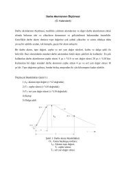
TURN-OFF SNUBBER<br />
Here is an example for turn-off<br />
snubber:<br />
Suppose that there is a buck<br />
converter with V dc = 400V, I dc =<br />
50A and t f = 0.5 µs.
•<br />
TURN-OFF SNUBBER
TURN-OFF SNUBBER<br />
If the transistor is operated<br />
near its rating, the SOA can<br />
easily be exceeded, with<br />
respect to both peak power<br />
and second-breakdown limits.
TURN-OFF SNUBBER<br />
So, if either the peak or the<br />
average power dissipation are<br />
too high for the transistors, or<br />
if the SOA is exceeded by<br />
switching the transistor, a turnoff<br />
snubber must be used to<br />
change the waveforms. The<br />
capacitor C s is a simpler<br />
snubber. Now when the<br />
transistor is turned off, its<br />
voltage and current waveforms<br />
look like shown in the figure.
TURN-OFF SNUBBER<br />
Note that because C s supplies a third path through which I dc<br />
can flow, it is no longer necessary for v Q to rise to equal V dc<br />
before i Q can begin to fall as the diode picks up the load<br />
current. Instead, any difference between I dc and i Q flows<br />
through C s . The charging of this capacitor, rather than the<br />
switching time of the transistor, governs the rate at which v Q<br />
rises from zero to V dc .
TURN-OFF SNUBBER<br />
Because the voltage across C s increases at a rate proportional<br />
to 1/C s , we can choose a large enough capacitor to keep the rise<br />
in voltage to only a small fraction, γ v , of V dc by the time i Q<br />
reaches zero. The consequence of including C s is that the peak<br />
power and total dissipation in the transistor are much smaller<br />
than they were below before the inclusion of C s , as illustrated by<br />
the bottom graph.
TURN-OFF SNUBBER<br />
In addition to the reducing the<br />
dissipation in the transistor,<br />
the snubber capacitor also<br />
maintains the switching locus<br />
in the SOA of the transistor.<br />
The bottom figure shows the<br />
turn-off locus as modified by<br />
the presence of C s and turn-on<br />
locus by a snubber as well.
•<br />
CHOOSING A VALUE FOR C S
CHOOSING A VALUE FOR C S<br />
If we choose C s so that γ v =0.2 for<br />
V dc =400V, I dc =50A, and if we<br />
assume that t’ f =0.33µs, then<br />
W diss =0.12mJ. During the time<br />
0
A MORE PRACTICAL TURN-OFF SNUBBER<br />
A capacitor by itself is not a sufficient turn -off snubber because, when<br />
the transistor is turned on again, C s will discharge through Q.The<br />
resulting transistor current can be very large and lead to failure. To<br />
avoid this problem, we add resistor and a diode to C s , as shown above.<br />
The purpose of the resistance R s is to limit the discharge current when<br />
the transistor turned on, and the purpose of the diode D s is to allow<br />
the charging current to bypass the resistor during the turn -off<br />
transition.
A MORE PRACTICAL TURN-OFF SNUBBER<br />
A tradeoff is necessary in determining the value of R s , It must be<br />
small enough to ensure that the capacitor is fully discharged during<br />
the shortest time that Q might be on but large enough to prevent the<br />
discharge current from exceeding the transistor rating.
TURN-ON SNUBBER<br />
The figure on the side shows<br />
the voltage and current<br />
waveforms during the turn-on<br />
in the transistor. Just like the<br />
turn-off snubber, the turn-on<br />
snubber serves to modify the<br />
switching waveforms to<br />
reduce the loss and maintain<br />
operation within the SOA.
TURN-ON SNUBBER<br />
Dissipation during the turn-on<br />
transition can be calcutated,<br />
just like the way that is found<br />
while turn-off dissipation, with<br />
t f replaced by t r . A typical value<br />
of i r , for a 400V 50A transistor<br />
is 0.5 µs. This value for t r<br />
results in a peak power of<br />
20kW and an energy loss of<br />
5mJ during each turn-on<br />
transition. With a switching<br />
frequency of 20 kHz, turn-on<br />
causes 100W of dissipation in<br />
the transistor.
TURN-ON SNUBBER<br />
The switching locus in the i Q -v Q<br />
plane for this transition is<br />
identical to the one shown on<br />
turn-off, except that the path<br />
is taken in the reverse<br />
direction. Once again, the<br />
transistor’s peak power and<br />
second-breakdown limits are<br />
exceeded.
TURN-ON SNUBBER<br />
The solution to the turn-on<br />
problem is the dual of the turnoff<br />
problem solution. A<br />
snubber, L s , is placed in series<br />
with the transistor. The<br />
waveforms are shown on the<br />
side.
•<br />
TURN-ON SNUBBER
TURN-ON SNUBBER<br />
At the switching frequency of<br />
20 kHz, the resulting average<br />
turn-on dissipation in the<br />
transistor is 1.2. That quantity<br />
is almost 1/100 of the turn-on<br />
losses without a snubber.<br />
The peak power is also<br />
reduced, and the turn-on<br />
swtitching locus now remains<br />
within the SOA.
A MORE PRACTICAL TURN-ON SNUBBER<br />
As with the turn-off snubber, the turn-on snubber requires additional<br />
components to allow the transistor to survive. In this case, if nothing<br />
were added to the circuit, the transistor would recieve an impulse of<br />
voltage when it turned off, because the inductor current would be<br />
forced to change in a very short time. To avoid this potentially<br />
destructive transient, a resistor and a diode can be added to the<br />
snubber circuit, as shown above.The resistor R s provides an alternative<br />
path for the inductor current when the transistor turns off. The purpose<br />
of the D s is to keep the resistor from conducting during the turn-on<br />
transition
A MORE PRACTICAL TURN-ON SNUBBER<br />
The resistance R s must be large enough to completely discharge<br />
L s during the off state. However to minimize the transistor’s<br />
voltage stress, it should not be made any larger than necessary.
CHOOSING A VALUE FOR L S<br />
•
CHOOSING A VALUE FOR L S<br />
If the shortest time that we expect the transistor to be turned<br />
off is 2.5µs, or 5% of a 20 kHz cycle, we need an L s /R s time<br />
constant of about 0.5 µs to ensure that L s is completely<br />
discharged. Meeting this condition requires a resistor of value<br />
R s ≈ 2.5 Ω.
COMBINED TURN-ON&TURN-OFF<br />
SNUBBERS<br />
A combined turn-on&turn-off snubber circuit with the resistor<br />
placed to discharge C s and the voltage and current waveforms at<br />
turn off.
COMBINED TURN-ON&TURN-OFF<br />
SNUBBERS<br />
A combined turn-on&turn-off snubber circuit with the resistor<br />
placed to discharge L s and the voltage and current waveforms at<br />
turn on.