Focused ion beam technology, capabilities and ... - FEI Company
Focused ion beam technology, capabilities and ... - FEI Company
Focused ion beam technology, capabilities and ... - FEI Company

Create successful ePaper yourself
Turn your PDF publications into a flip-book with our unique Google optimized e-Paper software.
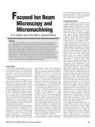
Figure 6: High-resolut<strong>ion</strong> SE image by <strong>ion</strong> <strong>beam</strong> scanning of a gold<br />
on carbon sample. Also note the strong crystal grain contrast within<br />
the gold particles. Horizontal field width is 1.5 µm.<br />
FIB <strong>and</strong> SEM instrumentat<strong>ion</strong><br />
As electrons <strong>and</strong> <strong>ion</strong>s are both charged<br />
particles, a focused <strong>ion</strong> <strong>beam</strong> system<br />
<strong>and</strong> an electron <strong>beam</strong> system such as<br />
a SEM have much in common:<br />
vacuum, lens control, electronics,<br />
scanning <strong>and</strong> patterning facility,<br />
electron detect<strong>ion</strong>, PC control, stage,<br />
etc. The instruments therefore have a<br />
similar design as is shown in figure 8.<br />
Some important differences in the<br />
design of FIB <strong>and</strong> SEM are:<br />
• Continuous use of a blanking signal<br />
for the <strong>ion</strong> <strong>beam</strong> column, when the<br />
<strong>beam</strong> is not used to collect an<br />
image or to induce the milling<br />
process. This is completely interlocked<br />
<strong>and</strong> automated with the<br />
control of the system to prevent<br />
undesired milling (e.g. during<br />
imaging). For the SEM this kind of<br />
funct<strong>ion</strong>ality is mostly applied only<br />
for e-<strong>beam</strong> lithography when<br />
unwanted exposure of e-<strong>beam</strong> resist<br />
must be avoided.<br />
• Control of the <strong>beam</strong> current in a<br />
SEM is done by selecting different<br />
demagnificat<strong>ion</strong> factors (lens control)<br />
for the column (changing the<br />
size of the <strong>beam</strong> at the posit<strong>ion</strong> of<br />
the aperture). Control of the <strong>ion</strong><br />
<strong>beam</strong> current is realized by selecting<br />
different apertures (changing<br />
the size of the aperture at a fixed<br />
posit<strong>ion</strong> in the <strong>beam</strong>). For the <strong>ion</strong><br />
<strong>beam</strong> each of the selected apertures<br />
has an optimized performance at a<br />
certain lens setting <strong>and</strong> therefore,<br />
the more apertures, the more optimized<br />
the system will behave over<br />
the full <strong>beam</strong> current range.<br />
• The milling aspects of the FIB are<br />
so important that patterning is a<br />
st<strong>and</strong>ard capability of the system.<br />
For a SEM, patterning is mainly<br />
added for the sake of e-<strong>beam</strong> lithography.<br />
• The type of detectors that can be<br />
applied: SEM <strong>and</strong> FIB both have a<br />
Figure 7: Ion image of a chromium coated steel wire, showing very strong<br />
contrast of the metallic grains, due to their orientat<strong>ion</strong>s.<br />
secondary electron detector, SEM<br />
may have a back scatter electron<br />
detector, a STEM detector <strong>and</strong> /or<br />
an x-ray detector, whereas FIB has<br />
an <strong>ion</strong> detector. Both systems can<br />
also use the sample current as a<br />
signal.<br />
• FIB can be equipped with an <strong>ion</strong><br />
flood gun to greatly reduce the<br />
charging of insulating samples.<br />
As can be derived from the intermezzo,<br />
the charging induced by the<br />
<strong>ion</strong> <strong>beam</strong> is positive <strong>and</strong> any addit<strong>ion</strong>al<br />
negative charge can be used<br />
to compensate this. One way that<br />
conveniently compensates the<br />
charge is the use of a flood gun: a<br />
low-energy, non focused spray of<br />
electrons that compensates the<br />
positive charge on the surface.<br />
7