Focused ion beam technology, capabilities and ... - FEI Company
Focused ion beam technology, capabilities and ... - FEI Company
Focused ion beam technology, capabilities and ... - FEI Company

You also want an ePaper? Increase the reach of your titles
YUMPU automatically turns print PDFs into web optimized ePapers that Google loves.
<strong>Focused</strong> <strong>ion</strong> <strong>beam</strong> <strong>technology</strong>, <strong>capabilities</strong><br />
<strong>and</strong> applicat<strong>ion</strong>s<br />
A focused <strong>ion</strong> <strong>beam</strong> system (FIB) is a relatively new tool that has a high degree of analogy with a focused<br />
electron <strong>beam</strong> system such as a scanning electron microscope or a transmiss<strong>ion</strong> electron microscope.<br />
In these systems the electron <strong>beam</strong> is directed towards the sample, <strong>and</strong> upon interact<strong>ion</strong> it generates<br />
signals that are used to create high magnificat<strong>ion</strong> images of the sample. As the <strong>beam</strong> is well controlled in<br />
size <strong>and</strong> posit<strong>ion</strong> <strong>and</strong> the signals are strong enough to be detected without excessive noise, these kinds<br />
of tools are very powerful to analyze samples in great detail over a wide range of magnificat<strong>ion</strong>s.<br />
The major difference with a focused <strong>ion</strong> <strong>beam</strong><br />
system is the use of a different particle to create<br />
the primary <strong>beam</strong> that interacts with the sample.<br />
As the name FIB indicates, <strong>ion</strong>s are used instead of<br />
electrons.<br />
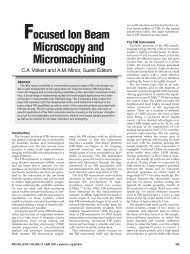
Figure 1: Ion <strong>beam</strong> induced SE image of a<br />
tungsten defect underneath an aluminum<br />
layer on a semi-conductor device.<br />
Figure 2: SE image (low current FIB) of an<br />
uncoated pollen grain, cut by the <strong>ion</strong> <strong>beam</strong><br />
(at high current).<br />
In a scanning electron microscope (SEM), electrons<br />
are accelerated <strong>and</strong> focused onto the sample<br />
surface. The <strong>beam</strong> can be scanned over the sample<br />
surface to create an image, or can be controlled<br />
by a patterning funct<strong>ion</strong> to locally expose the sample<br />
to the <strong>beam</strong>, as for example used in e-<strong>beam</strong><br />
lithography. These same basic funct<strong>ion</strong>alities are<br />
found in a focused <strong>ion</strong> <strong>beam</strong> system.<br />
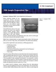
Figure 3: Phase of TEM sample preparat<strong>ion</strong><br />
on a sample of a voided SiC composite<br />
material.<br />
3