Focused ion beam technology, capabilities and ... - FEI Company
Focused ion beam technology, capabilities and ... - FEI Company Focused ion beam technology, capabilities and ... - FEI Company
18 Figure 49: SE image made with ion beam of catalyst covered ceramic balls. The use of FIB allows any individual particle to be selected and analyzed for industrial quality control. In this case the FIB has machined a TEM sample of the top surface. Time to result: 60 minutes. FIB systems deliver a single instrumental solution to enhance the speed and quality of the IC production process. The capability to perform design edits to the fabricated circuit ensures that the design and debug phase is limited to one mask step, and that extensive and expensive iteration steps can be avoided. The process control and failure analysis capabilities offered by FIB also provide the fastest possible route-cause data to shorten yield improvement cycles and solve site specific failure modes, either in the production process or on customer returns. On-Chip Circuit Editing Precision focused ion beam (FIB) milling and deposition enable the editing of existing circuits to shortcut the debug and test cycle. Advanced FIB techniques facilitate the editing of deep sub-micron technologies, planarized devices and flip chip packaged parts. FIB circuit changes are done by opening circuit nodes from the top, then connecting these nodes together by depositing metal over the top insulator into these new vias, and finally cutting unwanted tracks. FIB Via Milling Circuit nodes are accessed from the top using precision FIB milling. 1 2 3 4 Milling new vias to four select circuit nodes Figure 50: Secondary electron image made with the ion beam of a cross-section into a sintered magnet. Note that imaging with the ion beam and the milling process are unaffected by highly magnetic material because the sensitivity to magnetic fields is low (lower than for electrons). The cutting edge for semiconductor laboratory applications FIB Metal Deposition New connections are added using FIB deposition (1), and the original path of the circuitry is cut (2). The new circuit design is now ready for testing/debug. 1 - Tungsten deposition strap 2 - Isolation cut Track Crossing Multiple layer circuit edits can be performed by using FIB deposited insulator deposition Exclusive CoppeRx process for milling of copper parts With CoppeRx Without CoppeRx Figure 51: The steel sample has been crosssectioned both longitudinally and transversely by the ion beam at the same location, showing elongated grains on the left and truncated grains on the right. Ion beam channeling contrast of grain sizes is possible down to the 50 nm scale. GDSII Navigation Overlay your design and make changes realtime with CAD overlay FIB permits direct signal probing for electrical or Electron Beam testing even on signals covered by toplayer metal
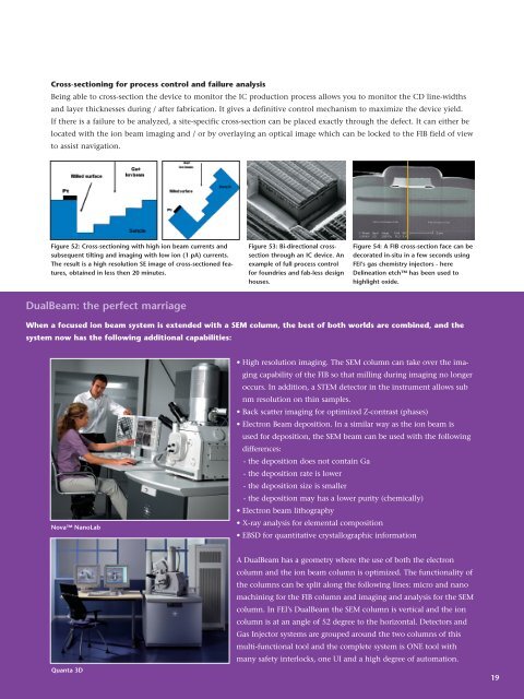
Cross-sectioning for process control and failure analysis Being able to cross-section the device to monitor the IC production process allows you to monitor the CD line-widths and layer thicknesses during / after fabrication. It gives a definitive control mechanism to maximize the device yield. If there is a failure to be analyzed, a site-specific cross-section can be placed exactly through the defect. It can either be located with the ion beam imaging and / or by overlaying an optical image which can be locked to the FIB field of view to assist navigation. Figure 52: Cross-sectioning with high ion beam currents and subsequent tilting and imaging with low ion (1 pA) currents. The result is a high resolution SE image of cross-sectioned features, obtained in less then 20 minutes. DualBeam: the perfect marriage Nova NanoLab Figure 53: Bi-directional crosssection through an IC device. An example of full process control for foundries and fab-less design houses. Figure 54: A FIB cross-section face can be decorated in-situ in a few seconds using FEI’s gas chemistry injectors - here Delineation etch has been used to highlight oxide. When a focused ion beam system is extended with a SEM column, the best of both worlds are combined, and the system now has the following additional capabilities: Quanta 3D • High resolution imaging. The SEM column can take over the imaging capability of the FIB so that milling during imaging no longer occurs. In addition, a STEM detector in the instrument allows sub nm resolution on thin samples. • Back scatter imaging for optimized Z-contrast (phases) • Electron Beam deposition. In a similar way as the ion beam is used for deposition, the SEM beam can be used with the following differences: - the deposition does not contain Ga - the deposition rate is lower - the deposition size is smaller - the deposition may has a lower purity (chemically) • Electron beam lithography • X-ray analysis for elemental composition • EBSD for quantitative crystallographic information A DualBeam has a geometry where the use of both the electron column and the ion beam column is optimized. The functionality of the columns can be split along the following lines: micro and nano machining for the FIB column and imaging and analysis for the SEM column. In FEI’s DualBeam the SEM column is vertical and the ion column is at an angle of 52 degree to the horizontal. Detectors and Gas Injector systems are grouped around the two columns of this multi-functional tool and the complete system is ONE tool with many safety interlocks, one UI and a high degree of automation. 19
- Page 1: Focused ion beam technology, capabi
- Page 4 and 5: Technology 4 Electrons replaced by
- Page 6 and 7: 6 Useful signals As many signals ar
- Page 8 and 9: 8 Anode Lens 1 Scan & Stig Coils El
- Page 10 and 11: 10 Deposition As FIB technology is
- Page 12 and 13: 12 Figure 21: Cantilever with proof
- Page 14 and 15: Application examples 14 The New Dim
- Page 16 and 17: 16 Figure 42: FIB machined photonic
- Page 20: FEI Company World Headquarters and
Cross-sect<strong>ion</strong>ing for process control <strong>and</strong> failure analysis<br />
Being able to cross-sect<strong>ion</strong> the device to monitor the IC product<strong>ion</strong> process allows you to monitor the CD line-widths<br />
<strong>and</strong> layer thicknesses during / after fabricat<strong>ion</strong>. It gives a definitive control mechanism to maximize the device yield.<br />
If there is a failure to be analyzed, a site-specific cross-sect<strong>ion</strong> can be placed exactly through the defect. It can either be<br />
located with the <strong>ion</strong> <strong>beam</strong> imaging <strong>and</strong> / or by overlaying an optical image which can be locked to the FIB field of view<br />
to assist navigat<strong>ion</strong>.<br />
Figure 52: Cross-sect<strong>ion</strong>ing with high <strong>ion</strong> <strong>beam</strong> currents <strong>and</strong><br />
subsequent tilting <strong>and</strong> imaging with low <strong>ion</strong> (1 pA) currents.<br />
The result is a high resolut<strong>ion</strong> SE image of cross-sect<strong>ion</strong>ed features,<br />
obtained in less then 20 minutes.<br />
DualBeam: the perfect marriage<br />
Nova NanoLab<br />
Figure 53: Bi-direct<strong>ion</strong>al crosssect<strong>ion</strong><br />
through an IC device. An<br />
example of full process control<br />
for foundries <strong>and</strong> fab-less design<br />
houses.<br />
Figure 54: A FIB cross-sect<strong>ion</strong> face can be<br />
decorated in-situ in a few seconds using<br />
<strong>FEI</strong>’s gas chemistry injectors - here<br />
Delineat<strong>ion</strong> etch has been used to<br />
highlight oxide.<br />
When a focused <strong>ion</strong> <strong>beam</strong> system is extended with a SEM column, the best of both worlds are combined, <strong>and</strong> the<br />
system now has the following addit<strong>ion</strong>al <strong>capabilities</strong>:<br />
Quanta 3D<br />
• High resolut<strong>ion</strong> imaging. The SEM column can take over the imaging<br />
capability of the FIB so that milling during imaging no longer<br />
occurs. In addit<strong>ion</strong>, a STEM detector in the instrument allows sub<br />
nm resolut<strong>ion</strong> on thin samples.<br />
• Back scatter imaging for optimized Z-contrast (phases)<br />
• Electron Beam deposit<strong>ion</strong>. In a similar way as the <strong>ion</strong> <strong>beam</strong> is<br />
used for deposit<strong>ion</strong>, the SEM <strong>beam</strong> can be used with the following<br />
differences:<br />
- the deposit<strong>ion</strong> does not contain Ga<br />
- the deposit<strong>ion</strong> rate is lower<br />
- the deposit<strong>ion</strong> size is smaller<br />
- the deposit<strong>ion</strong> may has a lower purity (chemically)<br />
• Electron <strong>beam</strong> lithography<br />
• X-ray analysis for elemental composit<strong>ion</strong><br />
• EBSD for quantitative crystallographic informat<strong>ion</strong><br />
A DualBeam has a geometry where the use of both the electron<br />
column <strong>and</strong> the <strong>ion</strong> <strong>beam</strong> column is optimized. The funct<strong>ion</strong>ality of<br />
the columns can be split along the following lines: micro <strong>and</strong> nano<br />
machining for the FIB column <strong>and</strong> imaging <strong>and</strong> analysis for the SEM<br />
column. In <strong>FEI</strong>’s DualBeam the SEM column is vertical <strong>and</strong> the <strong>ion</strong><br />
column is at an angle of 52 degree to the horizontal. Detectors <strong>and</strong><br />
Gas Injector systems are grouped around the two columns of this<br />
multi-funct<strong>ion</strong>al tool <strong>and</strong> the complete system is ONE tool with<br />
many safety interlocks, one UI <strong>and</strong> a high degree of automat<strong>ion</strong>.<br />
19


