Focused ion beam technology, capabilities and ... - FEI Company
Focused ion beam technology, capabilities and ... - FEI Company
Focused ion beam technology, capabilities and ... - FEI Company

You also want an ePaper? Increase the reach of your titles
YUMPU automatically turns print PDFs into web optimized ePapers that Google loves.
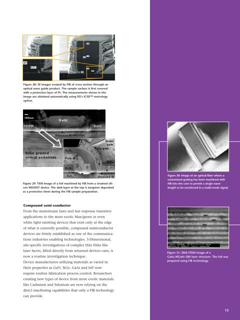
Figure 28: SE images created by FIB of cross-sect<strong>ion</strong> through an<br />
optical wave guide product. The sample surface is first covered<br />
with a protective layer of Pt. The measurements shown in the<br />
image are obtained automatically using <strong>FEI</strong>’s IC3D metrology<br />
opt<strong>ion</strong>.<br />
Figure 29: TEM image of a foil machined by FIB from a strained silicon<br />
MOSFET device. The dark layer at the top is tungsten deposited<br />
as a protective sheet during the FIB sample preparat<strong>ion</strong>.<br />
Compound semi-conductor<br />
From the mainstream laser <strong>and</strong> fast response transistor<br />
applicat<strong>ion</strong>s to the more exotic blue/green or even<br />
white light emitting devices that exist only at the edge<br />
of what is currently possible, compound semiconductor<br />
devices are firmly established as one of the communicat<strong>ion</strong>s<br />
industries enabling technologies. 3-Dimens<strong>ion</strong>al,<br />
site-specific investigat<strong>ion</strong>s of complex thin films like<br />
laser facets, lifted directly from returned devices cans, is<br />
now a routine investigat<strong>ion</strong> technique.<br />
Device manufacturers utilizing materials as varied in<br />
their properties as GaN, SiGe, GaAs <strong>and</strong> InP now<br />
require routine fabricat<strong>ion</strong> process control. Researchers<br />
creating new types of device from more exotic materials<br />
like Cadmium <strong>and</strong> Selenium are now relying on the<br />
direct machining <strong>capabilities</strong> that only a FIB <strong>technology</strong><br />
can provide.<br />
Figure 30: Image of an optical fiber where a<br />
customized grating has been machined with<br />
FIB into the core to permit a single wavelength<br />
to be monitored in a multi-mode signal.<br />
Figure 31: SEM-STEM image of a<br />
GaAs/AlGaAs QW laser structure. The foil was<br />
prepared using FIB <strong>technology</strong>.<br />
13