Quanta™ DualBeam™ and SEM Family Brief - FEI Company
Quanta™ DualBeam™ and SEM Family Brief - FEI Company
Quanta™ DualBeam™ and SEM Family Brief - FEI Company

Create successful ePaper yourself
Turn your PDF publications into a flip-book with our unique Google optimized e-Paper software.
a n y w a y y o u l o o k a t i t ,<br />
f E i p r o v i d E s t h E w o r l d ’ s b E s t v i E w .<br />
Right the first time<br />
FiRst<br />
First to market<br />
Fast to volume<br />
Quanta DualBeam <br />
<strong>and</strong> <strong>SEM</strong> <strong>Family</strong><br />
Flexible Solutions for Sample<br />
Imaging in Semiconductor Labs<br />
The affordable <strong>SEM</strong> <strong>and</strong> DualBeam solution<br />
Technologies, materials <strong>and</strong> samples are changing across<br />
nodes at an ever-increasing rate, <strong>and</strong> so is the diagnostics<br />
function in analytical labs. To win the race to volume, not<br />
only do your analytical tools need to be reliable, they must<br />
accommodate very different materials while collecting<br />
more data in less time. Meanwhile, there is increasing<br />
dem<strong>and</strong> for nondestructive analysis <strong>and</strong> functionality<br />
that can accommodate advanced analytical requirements<br />
into the future. The Quanta family is ideally suited to go<br />
beyond where optical microscopes fall short. Offering an<br />
array of easy-to-use systems, the Quanta family can also<br />
deliver cost-effective sectioning, imaging, analyzing <strong>and</strong><br />
inspecting for a variety of samples. Advanced, flexible,<br />
highly affordable imaging <strong>and</strong> analytical solutions come<br />
easy with Quanta.<br />
Enjoy these key benefits across the family:<br />
• Fast <strong>and</strong> simple imaging for complete structural analysis<br />
• Seamless “point-<strong>and</strong>-click” transition between imaging modes<br />
• Multi-vacuum mode enables in-situ, dynamic experiments<br />
<strong>and</strong> imaging <strong>and</strong> analysis on any sample<br />
• Accurate, efficient <strong>and</strong> easy-to-use automation software<br />
• Speed your time to answer by eliminating the need for<br />
sample preparation<br />
• Versatile system allows a wide range of accessories for<br />
analysis <strong>and</strong> sample manipulation
p r o d u c t f a m i l y d a t a<br />
Applications:<br />
Failure Analysis<br />
Cross section<br />
High-res FIB milling <strong>and</strong> imaging<br />
HR-<strong>SEM</strong> imaging<br />
General purpose <strong>SEM</strong> imaging<br />
Low damage TEM sample preparation<br />
Wet sample/packaging analysis<br />
TEM prep automation<br />
X-Ray analysis<br />
CAD navigation<br />
Probe compatible<br />
Metal deposition<br />
Metal etch<br />
Dielectric etch<br />
Dielectric deposition<br />
STEM detector<br />
EMI active cancellation<br />
Circuit Edit<br />
Front-side edits<br />
Back-side edits<br />
Electrical feed-through for probes<br />
Characterization <strong>and</strong> Analysis<br />
STEM (low kV)<br />
St<strong>and</strong>ard<br />
Some capabilites<br />
Optional<br />
The Quanta series is capable of generating <strong>and</strong> collecting all available<br />
information from any type of sample material. The Quanta 3D includes<br />
the capability of an ion column for ion beam imaging, material<br />
removal <strong>and</strong> material deposition.<br />
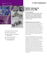
Versatile sample h<strong>and</strong>ling<br />
<strong>FEI</strong> developed the Quanta family to provide maximum<br />
imaging <strong>and</strong> microanalysis data on a wide range of<br />
samples, with or without preparation. In Quanta, you have<br />
a single tool with capabilities that used to require several<br />
systems. Making difficult samples suitable for conventional,<br />
high-vacuum scanning electron microscopy (<strong>SEM</strong>)<br />
environments is time consuming <strong>and</strong> can lead to<br />
unacceptable delays in the data-collection process. Across<br />
the family, Quanta features three imaging modes – high<br />
vacuum, low vacuum <strong>and</strong> environmental scanning electron<br />
microscopy (E<strong>SEM</strong>) – to significantly reduce your time to<br />
data by enabling analysis for the most difficult samples with<br />
one tool. The Quanta family also allows you to conduct<br />
analysis while leaving specimens intact for possible further<br />
investigation to complement the diagnostics dataset. You<br />
get repeatable, reliable results, ensuring the highest degree<br />
of accuracy from your data. Whatever your specific needs,<br />
you can predict a significant return on your investment,<br />
thanks to Quanta’s versatile sample h<strong>and</strong>ling.
Product E<strong>SEM</strong> Mode<br />
Low-Vacuum<br />
Mode<br />
High-Vacuum<br />
Mode<br />
<strong>SEM</strong><br />
Technology<br />
p r o d u c t f a m i l y d a t a<br />
FIB<br />
Technology<br />
Stage<br />
Travel<br />
Quanta 200 3.5 nm @ 30 kV 15 nm @ 3 kV 3.5 nm @ 30 kV Tungsten 50 mm<br />
Quanta 400 3.5 nm @ 30 kV 15 nm @ 3 kV 3.5 nm @ 30 kV Tungsten 100 mm<br />
Quanta 600 3.5 nm @ 30 kV 15 nm @ 3 kV 3.5 nm @ 30 kV Tungsten 150 mm<br />
Quanta 3D 200 3.5 nm @ 30 kV 15 nm @ 3 kV 3.5 nm @ 30 kV Tungsten Magnum 50 mm<br />
Quanta 200 FEG 2 nm @ 30 kV 3.5 nm @ 3 kV 3.5 nm @ 30 kV FEG 50 mm<br />
Quanta 400 FEG 2 nm @ 30 kV 3.5 nm @ 3 kV 2 nm @ 30 kV FEG 100 mm<br />
Quanta 600 FEG 2 nm @ 30 kV 3.5 nm @ 3 kV 2 nm @ 30 kV FEG 150 mm<br />
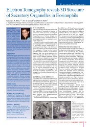
Quanta used to investigate contamination for quality control<br />
The Quanta FEG is capable of large field-of-view imaging <strong>and</strong> the<br />
low-vacuum mode enables the device to be kept uncoated during<br />
the analysis<br />
Package bump cross-sectioned in Quanta 3D <strong>and</strong> imaged with<br />
electron beam<br />
High-magnification image of transistor showing versatility of<br />
Quanta FEG
a n y w a y y o u l o o k a t i t ,<br />
f E i p r o v i d E s t h E w o r l d ’ s b E s t v i E w .<br />
Seeing more comes easy<br />
Easy to use, the Quanta family features a four-quadrant<br />
image display that simultaneously provides surface<br />
characterization <strong>and</strong> phase distribution through the live<br />
imaging of secondary electron (SE) <strong>and</strong> back-scattered<br />
electron (BSE) images. Switching imaging modes is as<br />
simple as a single mouse click. And the Quanta user<br />
interface offers embedded microanalysis to deliver results<br />
in the shortest time possible. What’s more, the highly<br />
versatile system can be equipped for further analysis<br />
with techniques such as energy dispersive spectrometry<br />
(EDS), wave dispersive x-ray spectrometry (WDS) <strong>and</strong><br />
electron backscattered diffraction (EBSD). The Quanta<br />
field emission <strong>SEM</strong> (FEG-<strong>SEM</strong>) can also be equipped<br />
with a scanning transmission electron microscopy (STEM)<br />
detector for bright-field <strong>and</strong> dark-field imaging of<br />
samples. Now you can enjoy fast <strong>and</strong> easy access to results<br />
that simply aren’t possible with an optical microscope.<br />
Fast, affordable cross-section capabilities<br />
When you need to extend <strong>SEM</strong> characterization below<br />
the surface, the Quanta 3D series complements your<br />
existing characterization laboratory tools <strong>and</strong> extends<br />
your applications range for three-dimensional character-<br />
ization, transmission electron microscopy (TEM) sample<br />
preparation <strong>and</strong> structural modification of sample surfaces<br />
at the nanoscale. For sectioning, imaging, analyzing <strong>and</strong><br />
inspecting packaged parts or other back-end samples that<br />
may be wet or dirty, the Quanta 3D is an ideal tool. A full<br />
DualBeam (FIB/<strong>SEM</strong>) equipped with a tungsten electron<br />
column, focused ion beam column <strong>and</strong> gas injector system,<br />
the Quanta 3D offers a highly cost-effective <strong>and</strong> reliable<br />
means of site-specific cross-sectioning, complex ion-beam<br />
patterning, material deposition <strong>and</strong> etching, as well as the<br />
imaging <strong>and</strong> analysis Quanta offers across the family.<br />
Quanta FEG images of lead frames. The flexible imaging arrangement<br />
allows imaging with more surface detail with the SE detector in<br />
low-vacuum mode, then imaging of the phase distribution in low<br />
vacuum with the BSE detector.<br />
A faster return on your technology investment<br />
By virtue of their quality components <strong>and</strong> functions, <strong>FEI</strong><br />
products such as those featured in the Quanta family, deliver<br />
reliable, superior solutions that provide an exceptional return<br />
on your technology investment. What’s more, a partnership<br />
with <strong>FEI</strong> means enjoying the peace of mind that comes from<br />
a long history of leading the industry with products that<br />
provide the highest-quality characterization, analytic <strong>and</strong><br />
metrology data in the shortest amount of time. <strong>FEI</strong> remains<br />
the only company offering the range of products necessary to<br />
address all of the imaging <strong>and</strong> sample preparation needs of<br />
today’s semiconductor lab. Now <strong>and</strong> in the future you can<br />
count on <strong>FEI</strong> to provide the most innovative, cost-effective<br />
solutions available for cross-sectional imaging, analysis <strong>and</strong><br />
sample preparation. Wherever you are on your technology<br />
roadmap, <strong>FEI</strong> remains committed to helping you get<br />
designs right the first time, get to market first <strong>and</strong> ramp<br />
to volume fast.<br />
See more at www.fei.com.<br />
<strong>FEI</strong> <strong>Company</strong><br />
World Headquarters <strong>and</strong><br />
North American Sales<br />
5350 NE Dawson Creek Drive<br />
Hillsboro, OR 97124-5793 USA<br />
Tel: +1 503 726 7500<br />
Fax: +1 503 726 7509<br />
e-mail: sales@feico.com<br />
www.fei.com<br />
European Sales<br />
Tel: +31 40 27 66 768<br />
Fax: +31 40 27 66 786<br />
Asia-Pacific Sales<br />
Tel: +65 6272 0050<br />
Fax: +65 6272 0034<br />
Japan Sales<br />
Tel: +81 3-3740-0970<br />
Fax: +81 3-3740-0975<br />
©2006. We are constantly improving the performance of our products, so all<br />
specifications are subject to change without notice. The <strong>FEI</strong> logo, Quanta, E<strong>SEM</strong>,<br />
Magnum <strong>and</strong> DualBeam are trademarks of <strong>FEI</strong> <strong>Company</strong>.<br />
03PB-FR0211