Chip Scale Review - July 2008
Chip Scale Review - July 2008
Chip Scale Review - July 2008

You also want an ePaper? Increase the reach of your titles
YUMPU automatically turns print PDFs into web optimized ePapers that Google loves.
<strong>July</strong> <strong>2008</strong><br />
• Photolithography for WLP<br />
• Wafer Bumping
Visit us at SEMICON West, Booth 7834
CONTENTS<br />
<strong>July</strong> <strong>2008</strong><br />
Volume 12, Number 5<br />
The International Magazine of <strong>Chip</strong>-<strong>Scale</strong> Electronics, Flip-<strong>Chip</strong> Technology,<br />
Optoelectronics Interconnection and Wafer-Level Packaging<br />
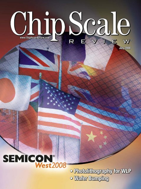
THE COVER<br />
In <strong>July</strong>, some days are quite memorable: <strong>July</strong> 4,<br />
America’s Independence Day; the first use of fingerprints<br />
for identification in <strong>July</strong> 1858; and Amelia Earhart’s 111th<br />
birthday on <strong>July</strong> 24 (Happy Birthday to you, Amelia!).<br />
Other events are both memorable and inevitable:<br />
I’m referring, of course, to SEMICON West!<br />
Although it’s only June as we write this, we’re already<br />
tingling with excitement over the arrival of SEMICON<br />
West as the dog days of summer begin. We’ve almost gotten<br />
used to the trek to San Francisco from San Jose.<br />
(Almost, but not quite, since we’re still trying to figure out<br />
the traffic patterns amid the one-way streets.)<br />
Like Dorothy in Oz, however, we still wish that we could<br />
somehow click our heels and be transported back to days of<br />
yore when SEMICON West was in the Magic Kingdom of the<br />
San Mateo County Fairgrounds. Sure, we sweated in those<br />
humongous portable gray structures in the backlot as the<br />
<strong>July</strong> sun boiled outside. But it was a mystical time for us and<br />
for the semiconductor industry. A time of inspired youth:<br />
we and the industry; a time we will, sadly, never recapture.<br />
But enough nostalgia and on to the present. We’re presenting<br />
several vital topics in this, our largest issue of the year.<br />
Terry Thompson presents his annual look at wafer bumping.<br />
Who knew a decade ago that “bumping” would have<br />
become an essential part of the industry’s vocabulary Not<br />
us—or we would have trademarked it! Bumping is now<br />
beyond mainstream and a significant profit center for<br />
equipment and materials makers.<br />
FEATURE ARTICLES<br />
Wafer-Bumping Services: What’s the 32<br />
Best Yardstick for Vendor Selection<br />
Terrence E. Thompson, Senior Editor<br />
Wafer bumping volume has built dramatically over the past few years<br />
and has become commonplace. A decade ago, you could select from a<br />
handful of providers; today, you have dozens. This article will help you<br />
select possible candidates for your bumped wafers.<br />
WLP Photolithography: The Tool Makers Tell 42<br />
You Why Their Machine Is the Right Choice<br />
Ron Iscoff, Editor<br />
Which tool for wafer-level packaging lithography is best We ask<br />
(and partially answer) that question nearly every year at this time.<br />
This year, we ask the tool makers themselves to give it their best shot.<br />
International Directory of Lithography Tools<br />
for Wafer-Level Packaging<br />
<strong>Chip</strong> <strong>Scale</strong> <strong>Review</strong> Staff<br />
48<br />
Driven by ‘Smartphones,’ Package-on-Package 51<br />
Adoption and Technology Are Ready to Soar<br />
Lee Smith, Amkor Technology Inc.<br />
As an enabling technology, package-on-package greatly expands<br />
device options by simplifying the business logistics of stacking and<br />
helps manage the cost impacts that derive from consumers’ increasing<br />
demands for multimedia processing and more memory.<br />
CONTINUED >><br />
Wafer-level photolithography ties rather nicely with wafer<br />
bumping. This time around we’re letting the principal WLP<br />
lithography tool makers have their say. Which, if history<br />
is any indication, it will be a contentious contest for<br />
who gets whose tool at a facility.<br />
We’ll see you in ‘Frisco. (They say, “Don’t call it ‘Frisco,’ but<br />
I was born there and I’m also in charge of filling this space<br />
and I can do what I want!) Enjoy the Big Show.<br />
(Illustration for <strong>Chip</strong> <strong>Scale</strong> <strong>Review</strong> by<br />
Design 2 Market) [design2marketinc.com]<br />
<strong>Chip</strong> <strong>Scale</strong> <strong>Review</strong>, at 7291 Coronado Dr., Suite 8, San Jose, CA 95129<br />
(ISSN 1526-1344), is published eight times a year, with issues in<br />
January-February, March, April, May-June, <strong>July</strong>, August-September,<br />
October and November-December.<br />
Periodical postage paid at San Jose, Calif., and additional offices.<br />
POSTMASTER: Send address changes to <strong>Chip</strong> <strong>Scale</strong> <strong>Review</strong> magazine,<br />
7291 Coronado Dr., Suite 8, San Jose, CA 95129.<br />
<strong>Chip</strong> <strong>Scale</strong> <strong>Review</strong> ■ <strong>July</strong> <strong>2008</strong> ■ [<strong>Chip</strong><strong>Scale</strong><strong>Review</strong>.com] 1
IC Assembly and Test<br />
Done Right and On Time<br />
Right: Expect high yields with the latest technology available.<br />
Above: The Signetics Paju, Korea, manufacturing facility<br />
Signetics has been exceeding customer expectations with<br />
on-time, cost-effective packaging solutions for 42 years!<br />
Since 1966, Signetics has been<br />
delivering assembly, packaging and<br />
test solutions that meet and exceed<br />
our customers’ requirements.<br />
From low-k 65nm wafers to stacked<br />
die and thermally enhanced packages,<br />
our expertise will help you stay at<br />
the leading edge.<br />
We’re especially proud of our capabilities in the<br />
assembly and test of logic and mixed-signal devices.<br />
Signetics is your BGA specialist!<br />
We’d like to demonstrate our proficiency<br />
in plastic packages—whether<br />
for ASIC, FPGA, memory or DSP applications.<br />
Please visit our web site at<br />
www.signetics.com to see our full<br />
line of QFP, FBGA/LGA, stacked die<br />
CSPs, PBGA, EPBGA and leadframe packages.<br />
Put us to the test! Contact your nearest Signetics<br />
office for more information.<br />
KOREA<br />
Signetics Inc.<br />
483-3 Buphung-ri,<br />
Thanhyun-myun,<br />
Paju-si Gyungki-do,<br />
Korea 413-840<br />
Tel: +82-31-940-7681<br />
Contact: B.S. Yoon<br />
bsyoon@signetics.com<br />
Signetics High Technology Inc.<br />
200 Brown Road, Suite 300<br />
Fremont, CA 94539<br />
Tel: 408-907-0121<br />
Contact: Mike Stokman<br />
mstokman@signetics.com<br />
UNITED STATES<br />
Signetics High Technology Inc.<br />
9 Executive Circle, Suite 275<br />
Irvine, CA 92614<br />
Tel: 945-553-8102<br />
Contact: Christopher Zumba<br />
chris.zumba@signetics.com
CONTENTS<br />
FEATURE ARTICLES<br />
Case Study: Building a Two-<strong>Chip</strong> Stacked Package 58<br />
Fred Haring, John Jacobson, Chris Hoffarth,<br />
Syed Sajid Ahmad and Aaron Reinholz, NDSU<br />
Engineering a single package housing multiple<br />
chips stacked vertically one above the other is a<br />
common practice that results in smaller and more<br />
efficient packages for devices. This article describes<br />
a case history and the challenges faced in the<br />
design and manufacture of the package.<br />
International Directory of Wafer-Bumping Services<br />
<strong>Chip</strong> <strong>Scale</strong> <strong>Review</strong> Staff<br />
69<br />
Conventional IC Testing Can’t Keep Up with 75<br />
Today’s System-on-a-<strong>Chip</strong> Requirements<br />
Anthony Lum, Advantest America Inc.<br />
There’s only one way to meet the exploding demand for system-on-a-chip<br />
(SoC) testing, and that is by dramatically increasing throughput. In addition,<br />
packaging and test challenges were once<br />
considered from the vantage point of<br />
independent solutions, each addressing<br />
a unique problem set without reference to<br />
the other. We can no longer afford to be<br />
myopic regarding our test requirements.<br />
DEPARTMENTS<br />
Publishers’ Page Terrence E. Thompson<br />
Assembly Lines Ron Iscoff<br />
Test Patterns Paul M. Sakamoto<br />
Industry News<br />
Standards Mark S. Bird<br />
Product Showcase (Advertisement)<br />
My View Dave Loaney<br />
Industry Events<br />
Advertorial Section<br />
Socketology Mike Fedde<br />
What’s New!<br />
Inside Patents A. Jason Mirabito and Carol Peters<br />
Ad Index/More News/Sales Offices<br />
6<br />
9<br />
12<br />
15<br />
40<br />
46<br />
74<br />
79<br />
80<br />
87<br />
91<br />
95<br />
96<br />
<strong>Chip</strong> <strong>Scale</strong> <strong>Review</strong> ■ <strong>July</strong> <strong>2008</strong> ■ [<strong>Chip</strong><strong>Scale</strong><strong>Review</strong>.com] 3
SSEC Single Wafer<br />
Clean<br />
99% Particle Removal Efficiency at<br />
the 88 nm, 65 nm, and 45 nm Nodes<br />
High Velocity Fan Scrub<br />
US # 6,539,952<br />
Single Wafer Megasonic Scrub<br />
Single Wafer Processing<br />
Wafer production success comes only through a combination of<br />
effective processes and the systems to implement them. Solid State<br />
Equipment Corporation is committed to process—with precise, high<br />
throughput systems that will maximize your wafer production and<br />
support that optimizes your process.<br />
Rotary PVA Brush Scrub<br />
With advanced single wafer non-contact<br />
and contact cleans, SSEC systems can be<br />
configured exactly to your cleaning<br />
requirements. Using dilute chemistries, such<br />
as SC-1 1:1:300, SSEC cleaning processors<br />
have 99% particle removal efficiency at the<br />
88 nm, 65 nm, and 45 nm nodes, with<br />
30 nm particle size in development.<br />
SSEC 3300 systems can be equipped with up to twelve sealed<br />
processing modules, configured for high speed, parallel<br />
operation or complex, serial processes. Each module is fitted<br />
with the combination of high performance processing tools<br />
that meets your requirements. The system can run both<br />
200 mm and 300 mm wafers, and SEMI ® standard or thin<br />
wafers, without a tooling change; only a simple software<br />
recipe change is needed.<br />
SSEC 3305<br />
5 Processing<br />
Stations<br />
Backed by SSEC's worldwide service and support, an SSEC wafer<br />
processor is your complete solution. Contact us for a system built<br />
to your specific needs.<br />
SSEC 3310<br />
10 Processing<br />
Stations
wet processing<br />
Solvent Strip<br />
Immersion and Single<br />
Wafer Processing<br />
Etch<br />
Uniform, Selective Etching on<br />
Multiple Process Levels<br />
Coat/Develop<br />
Photolithography Clusters<br />
Solvent Immersion<br />
Backside/Bevel Cleaning<br />
Spin Coating<br />
High Pressure Spray<br />
Spray Etch<br />
Hot Plate Bake Processing<br />
High Pressure Needle Dispense<br />
Using only milliliters of solvent per wafer,<br />
SSEC solvent processors combine batch<br />
immersion and single wafer spray<br />
technology in one SEMI ® safety<br />
compliant, dry-in/dry-out system. High<br />
pressure sprays are entirely under closedloop<br />
control for flow, temperature, and<br />
dispense arm motions.<br />
High Pressure Flow Control<br />
Stream Flow Etch<br />
Whether your requirements are for Under<br />
Bump Etching, with almost no undercut, or<br />
for wafer thinning, SSEC’s patented single<br />
wafer tools achieve more controlled results<br />
and substantial COO reduction, compared<br />
to batch or alternative single wafer systems.<br />
SSEC’s exclusive WaferChek in-situ<br />
adaptive process control ensures an<br />
optimum etch on every wafer.<br />
Spray Coat<br />
Application-specific coat and develop<br />
clusters are configured for your exact<br />
process requirements, including thick<br />
resist processing. SSEC systems provide<br />
standard 95% uptime. The advanced<br />
machine control technology enables<br />
superior uniformity within wafer, wafer<br />
to wafer, and lot to lot, including<br />
complete data tracking and operation<br />
with programmable robotic sequencing.<br />
SSEC Compliance<br />
Pressure<br />
Time<br />
Ti Etch<br />
Al Etch<br />
SEMI ® S2-0703aE Safety<br />
SEMI S8-0705 Ergonomics<br />
FM 4910 Materials<br />
SECS GEM CCS 200 & 300<br />
CE Marked<br />
ETL Listed<br />
Cu Etch<br />
3300<br />
Solid State Equipment Corporation<br />
Phone: 215-328-0700<br />
Email: info@ssecusa.com<br />
www.ssecusa.com
PUBLISHERS’ PAGE<br />
SEMICON West Redux:<br />
Please Do Spare the Energy!<br />
By Terrence E. Thompson, Co-Publisher and Senior Editor<br />
[tethompson@aol.com]<br />
Once again it’s show time for the semiconductor industry’s largest U.S. trade<br />
show: SEMICON West <strong>2008</strong> [semi.org]. From <strong>July</strong> 14-18, <strong>2008</strong>, exhibits, programs<br />
and visitors will dominate San Francisco’s Moscone Center and environs.<br />
Exhibits run <strong>July</strong> 15-17, and the focus of <strong>Chip</strong> <strong>Scale</strong> <strong>Review</strong>’s ongoing editorial coverage,<br />
test, assembly and packaging (TAP), will be located in West Hall levels 1 and 2.<br />
CSR’s booth is 7254 in the West Hall, Level 1. Please stop by and say hello.<br />
What do we know at press time TAP certainly is not alone this year in West Hall.<br />
SEMI has added a solar/photovoltaic (PV) show-in-a-show this year that will occupy<br />
much of the formerly barren third floor of the West building. Once again, SEMI organizers<br />
are looking at new markets in which SEMI members and show attendees can apply<br />
their IP and manufacturing skills to broaden customer bases and increase profitability.<br />
PV is part of SEMI’s expanded emphasis on nano-electronics applications and manufacturing<br />
which also includes:<br />
• Micro-electromechanical systems and microsystems (MEMS/MST) applications and<br />
manufacturing;<br />
• Energy technologies applications and manufacturing;<br />
• Fuel cells<br />
Major Change<br />
It certainly is a year of major change with sky-high energy costs forcing everyone to<br />
rethink what makes sense in the future. True, chipmakers and laboratories around the<br />
6<br />
Continued on page 30 >><br />
Add JCET to Your IC Packaging Foundry List<br />
We inadvertently failed to list Jiangsu Changjiang Electronics Technology Co.<br />
(JCET), China, in our April-May listing of packaging foundries.<br />
Jiangsu Changjiang Electronics<br />
Technology Co. (JCET), division of Xinchao<br />
Group, 275 Binjiang Middle Rd., Jiangyin City,<br />
Jiangsu Province, China 214431<br />
Phone: +86.510.8685.4189<br />
Fax: +86.510.8685.4550<br />
Chairman and CEO: Xinchao Wang<br />
President: Xiekang Yu<br />
Founded: 1972<br />
Web URL: www.cj-elec.com<br />
Contact for more info: Dr. Bill Li,<br />
General Manager, North American Operations,<br />
bli@jcet-us.com Phone: 510.573.3612<br />
U.S. Office: JCET North America,<br />
41341 Joyce Ave., Fremont, CA 94539<br />
<strong>Chip</strong> <strong>Scale</strong> <strong>Review</strong> ■ <strong>July</strong> <strong>2008</strong> ■ [<strong>Chip</strong><strong>Scale</strong><strong>Review</strong>.com]<br />
Stock Symbol: Shanghai Stock Exchange, 600584<br />
Revenue CY 2007 (USD): $330 million<br />
Revenue CY 2006 (USD): $240 million<br />
Number of employees: 7,000<br />
Customers by region: China, 100 percent<br />
Packaging materials used: Plastic<br />
Wafer bumping: Yes, plating and ball drop<br />
Flip-<strong>Chip</strong>: Yes RFID: Yes MEMS: Yes<br />
Total manufacturing area in square meters: 120,000<br />
Total facilities: 5, all in Jiangsu City<br />
X-ray inspection offered: Yes<br />
Test offered: analog/mixed signal, fine leak,<br />
gross leak, logic, memory, opens/shorts, RF<br />
Quality audits: ISO9001, ISO14000<br />
Highest volume package family assembled<br />
in 2007: SOT/SOD 2006: Same<br />
VOLUME 12, NUMBER 5<br />
The International Magazine of <strong>Chip</strong>-<strong>Scale</strong><br />
Electronics, Flip-<strong>Chip</strong> Technology, Optoelectronic<br />
Interconnection and Wafer-Level Packaging<br />
STAFF<br />
Gene Selven Publisher Emeritus, Special Projects Director<br />
7291 Coronado Dr., Ste. 8, San Jose, CA 95129<br />
b 408.996.7016 > 408.996.7871<br />
gselven@aol.com<br />
Kim Newman Co-Publisher/Sales Manager<br />
7291 Coronado Dr., Ste. 8, San Jose, CA 95129<br />
b 408.996.7016 > 408.996.7871<br />
csradv@aol.com<br />
Terrence Thompson Co-Publisher/Senior Editor<br />
2303 Randall Rd. #140, Carpentersville, IL 60110<br />
b 847.515.1255<br />
tethompson@aol.com<br />
Ron Iscoff Editor & Associate Publisher<br />
929 Ebbetts Ave., Manteca, CA 95337<br />
b 209.824.1289 > 209.644.7747<br />
chipscale@gmail.com<br />
Steve Berry Contributing Editor<br />
b 408.369.7000 > 408.369.8021<br />
saberry@electronictrendpubs.com<br />
Dr. Tom Di Stefano Contributing Editor<br />
b 408.321.8201 > 408.321.8701<br />
tom@centipedesystems.com<br />
Dr. Subash Khadpe Contributing Editor<br />
skhadpe@semitech.com<br />
Harvey S. Miller Contributing Editor-at-Large<br />
b 650.328.4550 > 650.327.2360<br />
h.miller@ieee.org<br />
Paul M. Sakamoto Contributing Editor–Test<br />
b 925.924.9110 x148<br />
paul.sakamoto@inovys.com<br />
Sandra Winkler Contributing Editor<br />
b 408.369.7000 > 408.369.8021<br />
slwinkler@electronictrendpubs.com<br />
The Official Publication of the WLCSP Forum<br />
SUBSCRIPTION INQUIRIES<br />
Judy Levin <strong>Chip</strong> <strong>Scale</strong> <strong>Review</strong><br />
7291 Coronado Dr., Ste. 8, San Jose, CA 95129<br />
b 408.996.7016 > 408.996.7871<br />
csrsubs@chipscalereview.com<br />
ADVERTISING PRODUCTION<br />
INQUIRIES AND REPRINTS<br />
Kim Newman<br />
7291 Coronado Dr., Ste. 8, San Jose, CA 95129<br />
b 408.996.7016 > 408.996.7871<br />
csradv@aol.com<br />
ADVISORS<br />
Mark DiOrio MTBSolutions<br />
Dr. Tom Di Stefano Centipede Systems<br />
Charles R. Harper Technology Seminars Inc.<br />
Nick Langston Ardent Concepts Inc.<br />
Dr. Guna Selvaduray San Jose State University<br />
Dr. Thorsten Teutsch Pac Tech USA<br />
Dr. David Tuckerman Tessera Technologies<br />
Professor C.P. Wong Georgia Tech<br />
Copyright © <strong>2008</strong> by Gene Selven & Associates Inc.<br />
<strong>Chip</strong> <strong>Scale</strong> <strong>Review</strong> (ISSN 1526-1344) is a registered trademark<br />
of Gene Selven & Associates Inc. Publishing headquarters are<br />
located at 7291 Coronado Drive, Suite 8, San Jose, CA 95129.<br />
All rights reserved.<br />
<strong>Chip</strong> <strong>Scale</strong> <strong>Review</strong> is published eight times a year.<br />
Subscriptions in the U.S. are available without charge to<br />
qualified individuals in the electronics industry. Subscriptions<br />
outside the U.S. (eight issues) by airmail are $60 per year to<br />
Canada or $60 to other countries. In the U.S., subscriptions<br />
by first class mail are $40 per year.
MicrobondDocfish –<br />
Soccer Cup <strong>2008</strong><br />
01883 www.aim.de<br />
Umicore AG & Co. KG<br />
Microbond - EPM<br />
Hanau · Singapore<br />
www.microbond.eu<br />
Visit us at our booth no. 8421<br />
and learn more about our<br />
MicrobondDocfish product series<br />
for bumping applications and …<br />
beat the champions in a<br />
Euro <strong>2008</strong> like competition!
ASSEMBLY LINES<br />
Dealing with the Information Glut Era<br />
and a Few Other Worrisome Matters<br />
By Ron Iscoff, Editor [chipscale@gmail.com]<br />
Remember when your mother<br />
urged you (while you tried to<br />
hide that unfinished mass of<br />
spinach or beets), “Now finish your<br />
plate! There are children starving in<br />
Whatsanamia (or Brazinque or<br />
Tachydermyville”).<br />
Now, Finish Your Plate!<br />
I never figured out how eating a vegetable<br />
that didn’t appeal to me would<br />
help solve the plight of those starving<br />
children, but at least it’s now possible to<br />
really “finish your plate!” An ecologically<br />
motivated company in Taiwan has developed<br />
a plate made from wheat flour. The<br />
purpose, of course, is to consume it!<br />
You probably think of Taiwan as the<br />
home of the two largest wafer foundries,<br />
TSMC and UMC. While surfing the<br />
web recently, I learned that a group of<br />
clever Taiwanese student-researchers<br />
recently met a government-issued challenge<br />
to develop a product that can be<br />
used as both a mouthwash and a dishwashing<br />
soap.<br />
No question that the Internet provides<br />
an amazing entrée to the world of<br />
information. The problem is how to<br />
digest all of it—or at least that small<br />
portion that interests you. The Internet<br />
has not only opened an unlimited treasure<br />
box of data, it has also led us into<br />
the Information Glut Era.<br />
What we really need now is not more<br />
Continued on page 11 >><br />
World Class Products and<br />
Services from the Experts<br />
in Silicon Valley!<br />
DS 15000<br />
High speed die sorting up to 15,000 UPH<br />
Provider of quickturn BGA package<br />
and SiP designs, prototypes<br />
and signal integrity solutions<br />
World-class manufacturer of<br />
high-productivity screen printing<br />
equipment for WLCSP<br />
One-stop packaging foundry<br />
for SiP devices, from product<br />
development through delivery<br />
PTA<br />
Packaging Foundry<br />
Full flip chip capability<br />
at up to 15,000 UPH<br />
Dual indexing for 24 h continuous run<br />
no more time waste due to leader, trailer, reel change<br />
DS 15000<br />
Pacific Gate Technologies is your Silicon Valley-based packaging consultant<br />
and technical sales representative for the electronics industry’s<br />
leading brands. We specialize in solving your SiP and WLCSP device<br />
problems to meet the specialized demands of the RF and wireless market.<br />
3697 Millplain Court<br />
San Jose, CA 95121<br />
Tel: 408/705-4721 Cell: 408/393-3615<br />
danny.fields@pacgate-us.com<br />
www.pacgate-us.com<br />
Flexibility to process various products<br />
like bumped dice, wafer level packages or molded leadless packages<br />
100% online quality inspection, high resolution camera<br />
including black coated wafers, moulded wafers or thin die applications<br />
100% inkless manufacturing<br />
due to wafer mapping ensure highest quality of the handled units<br />
Ready for the market revolution for<br />
WLCSP flip chip sorting<br />
info@muhlbauer.com www.muhlbauer.com<br />
<strong>Chip</strong> <strong>Scale</strong> <strong>Review</strong> ■ <strong>July</strong> <strong>2008</strong> ■ [<strong>Chip</strong><strong>Scale</strong><strong>Review</strong>.com] 9
SENJU SOLDER<br />
Working to Make Lead-Free Virtually<br />
“Pain-Free”<br />
Senju Comtek Corp.<br />
20300 Stevens Creek Blvd. #300<br />
Cupertino, CA 95014<br />
phone: (408) 446-7866 fax: (408) 253-2140<br />
email: sales@senjucomtek.com<br />
www.senjucomtek.com<br />
SMIC<br />
Senju Comtek Corp.
ASSEMBLY LINES<br />
Continued from page 9 >><br />
information, but a thing to handle it.<br />
I’m thinking of an avatar or doppelganger<br />
(double walker) that can take<br />
over this chore. No doubt an AI lab<br />
somewhere is on top of this right now!<br />
Google’s Noble Library Project<br />
One of the most successful companies<br />
of the Information Glut Era is arguably<br />
Silicon Valley-based Google, the dominant<br />
search engine. The company’s two<br />
founders are multi-billionaires—not at<br />
Bill Gates’ level, yet—but only a few<br />
steps away.<br />
In December 2004, Google<br />
announced it would include in its<br />
search database the full text of books<br />
from five of the world’s largest research<br />
libraries and “snippets” from books covered<br />
by copyright. This is a massive job,<br />
and one that is now underway.<br />
Oxford, Harvard, Stanford, the<br />
University of Michigan and the New<br />
York Public Library are the participants.<br />
And while you may think this noble<br />
project would not be controversial, I’m<br />
afraid you would be wrong.<br />
The main controversy, which has also<br />
sparked several lawsuits, deals with fair<br />
use of copyrighted works. Many publishers,<br />
including McGraw-Hill, say they<br />
want a bite of Google’s “snippet” pie.<br />
When the project is completed, users<br />
will be able to scan the complete text of<br />
all public domain materials—and there<br />
are millions. For books covered by<br />
copyright, only a few sentences, under<br />
what’s known as the “Fair Use Doctrine”<br />
will be available.<br />
Good deal, right Well, maybe!<br />
The Google Boys, Larry Page (left) and Sergey Brin,<br />
are the fifth richest people in the world. (Google)<br />
Remember the old saw, “There is no<br />
free lunch” Google, which has an<br />
employee cafeteria at its headquarters<br />
said to rival many fine restaurants,<br />
remembers, and you are probably going<br />
to find ads on or with full-text public<br />
domain books. In other words, you<br />
Continued on page 90 >><br />
More Performance... Aries ultra high frequency sockets have a mere 1 dB<br />
signal loss at up to 40 GHz!!! Center probe and Microstrip sockets deliver more<br />
than a half million insertions with no loss of electrical performance.<br />
More Choices... Aries offer a full range of sockets for handler-use, manual test and<br />
burn-in...for virtually every device type, including the highest density BGA and CSP<br />
packages. Choice of molded or machined sockets for center probe and Kapton<br />
interposer models, too!<br />
Less Cost... in addition to extremely competitive initial cost, Aries replacement<br />
parts and repair costs beat the competition, assuring you of lowest total cost<br />
of ownership.<br />
Less Wait... Aries can deliver the exact sockets you need within 6 weeks.<br />
So why settle Aries makes it easy to get the world's best<br />
test sockets. Call or visit our web site to find out how!<br />
ISO 9001<br />
Certified<br />
Bristol, PA 19007-6810<br />
(215) 781-9956 fax: (215) 781-9845<br />
e-mail: info@arieselec.com<br />
www.arieselec.com<br />
Sensible Solutions... Fast!<br />
<strong>Chip</strong> <strong>Scale</strong> <strong>Review</strong> ■ <strong>July</strong> <strong>2008</strong> ■ [<strong>Chip</strong><strong>Scale</strong><strong>Review</strong>.com] 11
TEST PATTERNS<br />
Choices: Used Versus New Test Engineers<br />
By Paul M. Sakamoto, Contributing Editor–Test [paul_sakamoto@comcast.net]<br />
In my last column, I dispensed<br />
some advice on buying used test<br />
equipment. This time we’ll venture<br />
further into recession countermeasures<br />
by examining “how to buy<br />
used test engineers.”<br />
Test engineers (TEs) are the folks that<br />
make the programs and design the<br />
interface hardware for your ATE.<br />
There are a number of sources for<br />
these skilled men and women, as there<br />
are for other engineering disciplines. As<br />
in most marketplaces, the prime sources<br />
come down to the broad categories of<br />
“new” and “used.”<br />
These can be roughly translated into<br />
NCG (new college graduate) and VET<br />
(Very Experienced in Test). Some may<br />
argue that there are a lot of other<br />
shades, but these are the big ones today.<br />
Acquiring Talent<br />
Now, I will assume you all think you<br />
know when and how to acquire your<br />
own NCG talent. To review, you get<br />
NCGs when you work in a larger company<br />
that has an HR department, and<br />
you have a year to break them in.<br />
You understand that if you are going<br />
to make the NCG a TE, you are going to<br />
have to sell the candidate on that idea<br />
after a lot of explanation. This is stuff<br />
that doesn’t show up in 99 percent of<br />
engineering schools. After all this, you<br />
spend a year training them and hope<br />
for the best.<br />
12<br />
<strong>Chip</strong> <strong>Scale</strong> <strong>Review</strong> ■ <strong>July</strong> <strong>2008</strong> ■ [<strong>Chip</strong><strong>Scale</strong><strong>Review</strong>.com]
What you will likely end up with is<br />
someone who views the program and<br />
the computer screen of their workstation<br />
as reality, and the hardware, tester and<br />
chip as an abstraction.<br />
The NCG may or may not even know<br />
how to use an oscilloscope. As a plus,<br />
the NCG will quickly understand and<br />
interface well with the EDA infrastructure<br />
at your company and will believe in<br />
simulations. As an added bonus, they<br />
can explain cell phone text messaging to<br />
you, so you can deal with intercepted<br />
messages to and from your kids.<br />
Another Story<br />
The VETs are another story. There are<br />
many routes for our VETs to have<br />
arrived at their current status. Many<br />
used to be NCGs and just stayed in test<br />
after their indoctrination. Others were<br />
Do you see your next NCG test engineer in this newly minted group<br />
technicians and maintenance personnel<br />
who had a bent for electronics and programming.<br />
Still others have come from<br />
the military (real vets), aerospace, consumer<br />
electronics, you name it.<br />
The TE skill requirements from the 70s<br />
through the 90s principally centered on<br />
Continued on page 78 >><br />
SuperButton and SuperSpring Contact Elements<br />
High current, high frequency, low inductance<br />
Flexible Design for All Your Engineering Needs • No NRE for Custom Footprints<br />
SuperButton Connector Technology<br />
SuperSpring Connector Technology<br />
Board-to-Board<br />
or Board-to-Flex<br />
Custom Interposers<br />
Land Grid Array<br />
Package-to-Board<br />
Sockets<br />
Engineering Programming & Test Sockets<br />
• Connector free—lengths down to 1.0mm<br />
• Array counts over 2,000<br />
• Pitches down to 0.5mm<br />
• Mating against BGA, LGA, QFN, CSP or flex<br />
sales@hcdcorp.com www.hcdcorp.com (408) 743-9700 x331<br />
Copyright © 2006 High Conection Density, Inc. All rights reserved. Information is subject to change without notice. “SuperSpring” and “SuperButton” are trademarks of High Connection Density, Inc.<br />
<strong>Chip</strong> <strong>Scale</strong> <strong>Review</strong> ■ <strong>July</strong> <strong>2008</strong> ■ [<strong>Chip</strong><strong>Scale</strong><strong>Review</strong>.com] 13
INDUSTRY NEWS<br />
New Ph.D. Says GaN Transistors Could Replace Silicon<br />
Troy, N.Y.—Is the future dim for<br />
silicon to continue as the dominant<br />
material for semiconductors<br />
A newly minted Ph. D. at the<br />
Renssalaer Polytechnic Institute<br />
believes it may be.<br />
Even before Dr. Weixiao Huang<br />
received his doctorate from RPI, his<br />
new transistor captured the attention<br />
of some of the biggest American<br />
and Japanese automobile companies,<br />
according to the university.<br />
The <strong>2008</strong> graduate’s invention,<br />
says RPI, could replace the silicon<br />
transistor for high-power and<br />
high-temperature electronics.<br />
Dr. Weixiao Huang invented a GaN MOSFET that<br />
may replace silicon in high-power applications.<br />
Unisem’s Guilmart Resigns<br />
to ‘Pursue Other Interests’<br />
Kuala Lumpur,<br />
Malaysia—Bruno<br />
Guilmart, 48, Unisem<br />
group’s chief executive<br />
officer and executive<br />
director, resigned in<br />
early June to “pursue<br />
other interests.”<br />
Bruno Guilmart C. H. Ang, Unisem<br />
group’s chief operating<br />
officer has taken over Guilmart’s tasks.<br />
According to the company’s official press<br />
release, Ang, 57, “will be leading Unisem moving<br />
forward. Unisem does not anticipate<br />
Continued on page 16 >><br />
Humble Roots<br />
Dr. Huang, who comes from humble<br />
roots as the son of farmers in rural<br />
China, is the inventor of a new transistor<br />
that uses the compound material<br />
gallium nitride (GaN), which has<br />
remarkable material properties.<br />
The new GaN transistor could<br />
reduce the power consumption and<br />
improve the efficiency of power<br />
electronic systems in everything<br />
from motor drives and hybrid vehicles<br />
to home appliances and defense<br />
equipment.<br />
“Silicon has been the workhorse in<br />
the semiconductor industry for last<br />
two decades,” Dr. Huang observes.<br />
Continued on page 20 >><br />
Intel, Samsung, TSMC Agree<br />
on 450mm Wafer Pilot Line<br />
San Jose—The two largest producers of<br />
semiconductor memory and the largest<br />
wafer foundry have agreed to collaborate<br />
on the transition to the next large wafer<br />
size, 450mm (18 inches) in diameter.<br />
Intel Corp., the memory leader, and<br />
Samsung Electronics, the second largest<br />
memory provider, with foundry Taiwan<br />
Semiconductor Manufacturing Co. (TSMC)<br />
have set a 2012 date for the larger wafers.<br />
SEMICON West Sojourners<br />
Thousands of interested industry folk will make the trip to Moscone Center to visit SEMICON West<br />
again this year. West Hall, in background, home of assembly, packaging and test, will be their<br />
destination. (<strong>Chip</strong> <strong>Scale</strong> <strong>Review</strong>)<br />
An Intel technician examines a 300mm wafer for<br />
defects. In 2012, the task will be literally and physically<br />
larger as 450mm wafers go online. (Intel Corp.)<br />
Continued on page 25 >><br />
INSIDE NEWS<br />
• University Researchers: Quantum Computers<br />
May Become Practical page 96<br />
<strong>Chip</strong> <strong>Scale</strong> <strong>Review</strong> ■ <strong>July</strong> <strong>2008</strong> ■ [<strong>Chip</strong><strong>Scale</strong><strong>Review</strong>.com] 15
INDUSTRY NEWS<br />
Unisem Continued from page 11 >><br />
any additional<br />
changes to the<br />
group’s organizational<br />
structure, nor<br />
will there be any disruptions<br />
to Unisem’s<br />
daily operations.”<br />
Guilmart, a<br />
C.H. Ang Parisian with master’s<br />
degrees in electronics<br />
and business, joined the company in<br />
November 2003, when it operated as<br />
Advanced Interconnect Technologies,<br />
headquartered in Batam, Indonesia.<br />
He replaced AIT founder Ralph<br />
Duceour, who founded the company as<br />
Advanced Microtronics Technology in<br />
1991. Duceour was also a founder of<br />
ASAT, Hong Kong.<br />
Earlier, Guilmart served as senior vice<br />
president of worldwide sales for Singaporebased<br />
Chartered Semiconductor, the world’s<br />
third largest wafer foundry.<br />
In October 1999, Hana Technologies<br />
Ltd., Hong Kong, a subsidiary of Thailand’s<br />
Hana Semiconductor; and AMT merged<br />
into AIT. At the time, the combined companies<br />
earned an estimated $300 million<br />
between the Batam and Hong Kong plants.<br />
About three years later, AIT closed its<br />
Hong Kong IC assembly and test facility.<br />
‘Crippled by Price Erosion’<br />
“The phased closure of the Hong Kong<br />
facility comes in response to a particularly<br />
difficult array packaging sector that has<br />
been crippled by severe price erosion<br />
and ongoing overcapacity, coupled with<br />
low customer- and end-user demand,”<br />
Duceour said at the time.<br />
In <strong>July</strong> 2007, AIT was acquired for<br />
about $70 million by Malaysia-based<br />
Unisem Group.<br />
The acquisition gave Unisem IC<br />
assembly facilities in the U.K. (the former<br />
Atlantic Semiconductor, once ASAT’s<br />
A sea of bonders occupies the assembly floor at Unisem,<br />
Batam, the former AIT facility near Singapore.<br />
European packaging facility); Chengdu,<br />
China; Ipoh, Malaysia and Batam.<br />
After the acquisition, Unisem said the<br />
new Unisem group would boast a workforce<br />
of 8,800, about 300 test systems<br />
and 1500 wire bonders.<br />
The enlarged Unisem said it anticipated<br />
a combined revenue of $322 million for<br />
the fiscal year ended Dec. 31, 2006. In its<br />
2007 annual report, the group reported<br />
a profit of approximately $23 million<br />
(MYR 119,612,139). [unisemgroup.com] ■<br />
<br />
<br />
<br />
<br />
<br />
<br />
<br />
<br />
<br />
<br />
<br />
<br />
<br />
<br />
<br />
<br />
<br />
<br />
<br />
<br />
<br />
<br />
<br />
<br />
16<br />
<strong>Chip</strong> <strong>Scale</strong> <strong>Review</strong> ■ <strong>July</strong> <strong>2008</strong> ■ [<strong>Chip</strong><strong>Scale</strong><strong>Review</strong>.com]
INDUSTRY NEWS<br />
PEOPLE IN THE NEWS<br />
‘Different Opinions’ Lead to Resignation of Infineon Chief<br />
Neibiberg, Germany—“Different opinions<br />
on the future strategic orientation of the<br />
company” have led to the resignation of<br />
Dr. Wolfgang Ziebart, 58, Infineon’s president<br />
and CEO.<br />
Peter Bauer,member<br />
of the semiconductor<br />
company’s<br />
management board,<br />
has been moved into<br />
the CEO post.<br />
During a late May<br />
board meeting,<br />
Peter Bauer according to an<br />
announcement from<br />
Infineon, the supervisory board “unanimously<br />
declared its vote of confidence<br />
for Chairman Max Dietrich Kley.”<br />
Dr. Ziebert became CEO four years<br />
ago. During his tenure, he formed a<br />
separate company, Qimonda, from the<br />
company’s memory business.<br />
With Dr. Ziebart’s departure, the<br />
management and supervisory boards<br />
said they will begin a new companywide<br />
program, IFX 10-Plus, which comprises<br />
three key points: margin<br />
improvement through consistent portfolio<br />
management; margin improvement<br />
through a strong cost-cutting in<br />
manufacturing; and margin improvement<br />
through increased organizational<br />
efficiency.<br />
Bauer, the new CEO, holds an engineering<br />
degree from the Technical<br />
University of Munich and began his<br />
professional career in the semiconductor<br />
division of Siemens AG.<br />
He became a member of the Infineon<br />
board in 1999 and has headed the automotive,<br />
industrial and multimarket<br />
business group.<br />
Hudgens Joins Corwil as<br />
Military/Aerospace Mgr.<br />
Milpitas, Calif.—<br />
Michael Hudgens<br />
has joined Corwil as<br />
business development<br />
manager-military/<br />
aerospace from<br />
Kyocera America. He<br />
received a bachelor’s<br />
Michael Hudgens degree in mechanical<br />
engineering from<br />
Washington University and an MBA<br />
from the University of Phoenix.<br />
He is currently serving as vice president–<br />
membership for the Florida chapter of<br />
IMAPS. [corwil.com]<br />
The company, formerly part of<br />
Siemens AG, boasts about 43,000<br />
employees worldwide, including 13,500<br />
Quimonda employees. [infineon.com]<br />
18<br />
<strong>Chip</strong> <strong>Scale</strong> <strong>Review</strong> ■ <strong>July</strong> <strong>2008</strong> ■ [<strong>Chip</strong><strong>Scale</strong><strong>Review</strong>.com]
The new epoxy Die Bonder 2100 xP<br />
Revolutionizing<br />
die attach<br />
SEMICON West, 15–17 <strong>July</strong> <strong>2008</strong><br />
West Hall 1F, Booth No. 7011<br />
Unsurpassed speed at 20 μm accuracy<br />
Leading edge machine concept<br />
Fastest time to yield<br />
Platform of the future<br />
Highest uptime<br />
As one of the leaders in die attach for more than two decades,<br />
Oerlikon Esec is committed to surpassing its customers’ needs by<br />
designing the most innovative and revolutionary die attach platform.<br />
Learn more about the revolution in die attach on our website:<br />
www.oerlikon.com/esec/revolution
INDUSTRY NEWS<br />
GaN Transistors Continued from page 15 >><br />
“But as power electronics get more sophisticated<br />
and require higher-performing<br />
transistors, engineers have been seeking<br />
an alternative, like gallium nitride-based<br />
transistors, that can perform better than<br />
silicon and in extreme conditions.”<br />
Silicon-Based Electronics<br />
Each household today likely contains<br />
dozens of silicon-based electronics. An<br />
important component of each of those<br />
electronics is usually a silicon-based<br />
transistor know as a silicon metal/oxide<br />
semiconductor field-effect transistor<br />
(silicon MOSFET).<br />
The GaN MOSFET could reduce dependence on fossil fuels, says<br />
Dr. Huang.<br />
To convert the electric energy to other<br />
forms as required, the transistor acts as<br />
a switch, allowing or disallowing the flow<br />
of current through the device.<br />
Dr. Huang first developed a new<br />
process that demonstrates an excellent<br />
GaN MOS (metal/oxide/GaN) interface.<br />
Engineers have known that GaN and<br />
other gallium-based materials have some<br />
extremely good electrical properties,<br />
much better than silicon.<br />
However, no useful GaN MOS transistor<br />
had been developed. Dr. Huang’s innovation,<br />
the first GaN MOSFET of its kind in<br />
the world, has already shown world-record<br />
performance according to its inventor.<br />
In addition, Huang has shown that<br />
his innovation can integrate several<br />
important electronic functions onto one<br />
chip like never before.<br />
“This will significantly simplify entire<br />
electronic systems,” Dr. Huang said. He<br />
has also designed and experimentally<br />
demonstrated several new, novel highvoltage<br />
MOS-gated FETs, which have<br />
lower power consumption, smaller chip<br />
size and higher power density than silicon<br />
MOSFETs.<br />
Global Reduction in Fuel Consumption<br />
The new transistors can greatly reduce<br />
energy loss, making energy conversion<br />
more efficient. “If these new GaN transistors<br />
replaced many existing silicon<br />
MOSFETs in power electronics systems,<br />
there would be global<br />
reduction in fossil fuel consumption<br />
and pollution,”<br />
Dr. Huang contends.<br />
The new GaN transistors<br />
can also allow the electronics<br />
system to operate in<br />
extremely hot, harsh, and<br />
high-power environments—<br />
even those that produce<br />
radiation. “Because it is so<br />
resilient, the device could<br />
open up the field of electronic<br />
engineering in ways<br />
that were not previously possible due to<br />
the limitations imposed by less tolerant<br />
silicon transistors,” he said.<br />
Dr. Huang has published more than<br />
15 papers, while a doctoral student in<br />
the Department of Electrical, Computer,<br />
and Systems Engineering at Rensselaer.<br />
Despite obvious difficulties, his parents<br />
worked tirelessly to give Huang the best<br />
possible educational opportunities, the<br />
new Ph. D. reports.<br />
When school wasn’t enough, Dr.<br />
Huang’s father woke him up early every<br />
morning to practice mathematical calculations<br />
without a calculator, instilling<br />
in him a lifelong appreciation for basic,<br />
theoretical mathematics and sciences.<br />
[news.rpi.edu/] ■<br />
20<br />
<strong>Chip</strong> <strong>Scale</strong> <strong>Review</strong> ■ <strong>July</strong> <strong>2008</strong> ■ [<strong>Chip</strong><strong>Scale</strong><strong>Review</strong>.com]
INDUSTRY NEWS<br />
MEMS Expert Added to<br />
Wednesday A.M. Panel<br />
San Jose—Dr. Eric<br />
Mounier, a worldclass<br />
expert on MEMS,<br />
has joined the<br />
International Wafer-<br />
Level Packaging<br />
Conference business<br />
and marketing panel<br />
Dr. Eric Mounier on Wednesday<br />
morning at 8:30.<br />
Dr. Mounier holds a Ph.D. in semiconductors,<br />
and is a co-founder of Yole<br />
Développement, a Lyon, France-based<br />
market research company. In addition<br />
to his market analysis of advanced packaging<br />
technologies, he is chief editor of<br />
Micronews, a monthly Yole publication<br />
devoted to micro- and nanotechnologies.<br />
Other panelists at this session are Dr.<br />
Dan Tracy of SEMI, Jan Vardaman of<br />
TechSearch International, and Jim Walker<br />
of the Gartner Group.<br />
The panel precedes Wednesday’s technical<br />
presentations and is free to all registrants<br />
and exhibitors. [iwlpc.org]<br />
Ruscev Succeeds Khandros<br />
as FormFactor’s Chief Exec<br />
Livermore, Calif.—<br />
FormFactor’s board<br />
has appointed Mario<br />
Ruscev, 51, currently<br />
president, as its next<br />
CEO, succeeding<br />
Igor Khandros, 53,<br />
who founded the<br />
Mario Ruscev company in 1993.<br />
Khandros will<br />
become executive<br />
chairman of the<br />
FormFactor board of<br />
directors, succeeding<br />
Jim Prestridge, 76,<br />
its current chairman,<br />
who will remain on<br />
Igor Khandros the FormFactor board<br />
of directors and<br />
become its lead independent director.<br />
<strong>Chip</strong> Cooling System Pipes H 2 O Between Stacks in 3D Packages<br />
IBM scientists say their new chip cooling method will improve computer performance while reducing the<br />
energy used to operate. (IBM Corp.)<br />
Zurich, Switzerland—IBM Labs in<br />
Zurich, and Berlin’s Fraunhofer Institute<br />
have jointly developed a prototype that<br />
integrates a cooling system into 3D<br />
chips by piping water directly between<br />
each layer in a chip stack.<br />
Used in computer chips, IBM says the<br />
development will advance Moore’s Law<br />
and “significantly reduce energy consumed<br />
by data centers.”<br />
“In order to exploit the potential of<br />
high-performance 3-D chip stacking,<br />
we need interlayer cooling,” explains<br />
Thomas Brunschwiler, project leader at<br />
IBM’s Zurich Research Lab. “Until now,<br />
nobody has demonstrated viable solutions<br />
to this problem.<br />
“As we package chips on top of each<br />
other to significantly speed a processor’s<br />
capability to process data, we have found<br />
that conventional coolers attached to<br />
the back of a chip don’t scale.”<br />
Typical 3D chip stacks would have an<br />
aggregate heat dissipation of nearly<br />
1Kw, 10x greater than the heat generated<br />
by a hotplate, with an area of 4cm 2<br />
and a thickness of about 1mm.<br />
Moreover, each layer poses an additional<br />
barrier to heat removal, IBM says.<br />
The researchers piped water into<br />
cooling structures as thin as a human<br />
hair (50 microns) between the individual<br />
chip layers to remove heat efficiently at<br />
the source.<br />
Because of the superior thermo-physical<br />
qualities of water, scientists were<br />
able to demonstrate a cooling performance<br />
of up to 180W/cm 2 per layer for a<br />
stack with a typical footprint of 4cm 2 .<br />
In the IBM experiments, scientists<br />
piped water through a 1 x 1cm test<br />
vehicle, which consisted of a cooling<br />
layer between two dies or heat sources.<br />
The cooling layer measures only about<br />
100 microns in height and is packed<br />
with 10,000 vertical interconnects per<br />
cm 2 . [ibm.com]<br />
Phoenix X-Ray Opening New<br />
West Coast Service Center<br />
Newark, Calif.—Phoenix X-Ray, acquired<br />
in October 2007 as part of GE’s Sensing &<br />
Inspection Technologies business, opened<br />
a new West Coast demo and customer<br />
service center here last month.<br />
The location features a fully equipped<br />
applications and demo lab with state-of<br />
the-art 2D and 3D x-ray and CT technology,<br />
as well as training facilities. [ge.com]<br />
Check out our digital edition at<br />
www.chipscalereview-digital.com<br />
<strong>Chip</strong> <strong>Scale</strong> <strong>Review</strong> ■ <strong>July</strong> <strong>2008</strong> ■ [<strong>Chip</strong><strong>Scale</strong><strong>Review</strong>.com]<br />
21
INDUSTRY NEWS<br />
Dow Corning Opens Solar Center to Drive New Aps<br />
Freeland, Mich.—Dow<br />
Corning Corp. recently<br />
opened a $3 million Solar<br />
Solutions Application<br />
Center here to collaborate<br />
with customers in<br />
the development and<br />
evaluation of materials<br />
used to make solar panels.<br />
The 2,508-square<br />
meter Center includes a<br />
laboratory, pilot equipment<br />
and testing facilities.<br />
A team of engineers and scientists<br />
will staff the Center, which has been<br />
designed to be expanded as needed.<br />
The Center is the latest in a series of<br />
solar-related investments by Dow Corning.<br />
In May 2007, Dow Corning<br />
announced a major expansion at its<br />
The Center will develop materials for making solar panels.<br />
joint venture, Hemlock Semiconductor.<br />
In September 2006, the company introduced<br />
a solar-grade silicon, the industry’s<br />
first commercially available feedstock<br />
derived from metallurgical silicon using<br />
a large-scale manufacturing processes.<br />
[dowcorning.com]<br />
V-CAPS Gains Vietnamese Investment Certification<br />
This is the statue of Ho Chi Minh in the city that was formerly known<br />
as Saigon, but is now named after “Uncle Ho.”<br />
Hanoi, Vietnam—Vietnam-<br />
<strong>Chip</strong>scale Advanced Packaging<br />
Services (V-CAPS)<br />
says it has received its investment<br />
certificate from the<br />
Vietnamese government<br />
which recognizes the company<br />
as a 100% foreignowned<br />
high tech venture.<br />
The certificate allows<br />
V-CAPS to move forward<br />
with plans to set up a 35,000<br />
square-meter semiconductor<br />
assembly and test facility at<br />
the Hoa Lac Hi-Tech Park (HHTP),<br />
approximately 30 kilometers outside<br />
Hanoi in Ha Tay province.<br />
“We are very excited about completing<br />
this major milestone<br />
for V-CAPS,” said<br />
Harry Rozakis,<br />
V-CAPS’ CEO/president.<br />
We have<br />
known for some<br />
time that locating in<br />
Vietnam marks the<br />
Harry Rozakis next logical progression<br />
for the semiconductor assembly<br />
and test business as it migrates across<br />
the Asia-Pacific region.”<br />
On completion, V-CAPS says it will<br />
join Intel in having one of the most<br />
advanced high-tech manufacturing<br />
facilities in Vietnam. In addition V-CAPS<br />
will have one of the cost effective and<br />
“green” factories in the outsourced semiconductor<br />
assembly and test market.<br />
V-CAPS anticipates becoming operational<br />
before the end of 2009.<br />
[v-capssemi.com]<br />
What<br />
are<br />
your<br />
current<br />
burn-in<br />
sockets<br />
missing<br />
<strong>Chip</strong> <strong>Scale</strong> <strong>Review</strong> ■ <strong>July</strong> <strong>2008</strong> ■ [<strong>Chip</strong><strong>Scale</strong><strong>Review</strong>.com] 23
INDUSTRY NEWS<br />
450mm Wafers Continued from page 15 >><br />
The three companies are<br />
among the top five users of<br />
wafers for semiconductors<br />
in the world.<br />
The companies say they<br />
will cooperate with the<br />
semiconductor industry to<br />
ensure that the “required<br />
components, infrastructure,<br />
and capability for a pilot<br />
wafer line are ready” by the<br />
target date, although no<br />
month has been released.<br />
The transition to larger<br />
wafers will enable continued<br />
growth of the semiconductor<br />
industry, they note, and<br />
will help maintain a reasonable<br />
cost structure for future<br />
integrated circuit manufacturing and<br />
applications.<br />
Double Si Surface Area<br />
The total silicon surface area of a 450mm<br />
wafer and the number of printed die is<br />
more than twice that of a 300mm wafer.<br />
The bigger wafers help lower the production<br />
cost per chip, the companies<br />
observe. Additionally, improved efficiency<br />
lowers the use of energy, water and other<br />
resources.<br />
For example, according to the companies’<br />
announcement, the conversion from<br />
200mm wafers to 300mm wafers helped<br />
reduce aggregate emissions per chip of<br />
air pollution, global warming gasses and<br />
water. Further reduction is expected<br />
with a transition to 450mm wafers.<br />
Intel, Samsung and TSMC indicate<br />
that the semiconductor industry can<br />
San Jose—The adoption of 450mm<br />
wafers (18 inches) by the semiconductor<br />
industry—spearheaded by Intel, Samsung<br />
and TSMC—will bring a Pandora’s box<br />
filled with new challenges.<br />
300mm Wafer<br />
450mm Wafer<br />
The smaller circle represents a 300mm wafer’s size compared<br />
proportionately to the forthcoming 450mm wafer.<br />
improve its return on investment and<br />
substantially reduce 450mm research<br />
and development costs by applying<br />
aligned standards, rationalizing changes<br />
from 300mm infrastructure and<br />
automation, and by working toward a<br />
common timeline.<br />
The companies also agree that a<br />
cooperative approach will help minimize<br />
risk and transition costs.<br />
In the past, migration to the next<br />
larger wafer size traditionally began a<br />
decade after the last transition.<br />
For example, the industry began the<br />
transition to 300mm wafers in 2001, a<br />
decade after the initial 200mm fabs<br />
were introduced in 1991. Keeping in<br />
line with the historical pace of growth,<br />
Intel, Samsung and TSMC agree that<br />
2012 is an appropriate target to begin<br />
the 450mm transition. [intel.com] ■<br />
Industry Adoption of Larger Wafers Brings New Questions<br />
By Ron Iscoff, Editor<br />
A position paper, Advantages and<br />
Challenges Associated with the Introduction<br />
of 450mm Wafers, published by the<br />
International Technology Roadmap for<br />
Continued on page 27 >><br />
Increased<br />
Signal<br />
Speed<br />
More Power<br />
Low<br />
Inductance<br />
Stable<br />
Resistance<br />
Higher<br />
Temperatures<br />
Increased<br />
Stroke<br />
Replaceable<br />
Pins<br />
<strong>Chip</strong> <strong>Scale</strong> <strong>Review</strong> ■ <strong>July</strong> <strong>2008</strong> ■ [<strong>Chip</strong><strong>Scale</strong><strong>Review</strong>.com] 25
INDUSTRY NEWS<br />
Larger Wafers Continued from page 25 >><br />
The<br />
Solution<br />
Intel Corp., is one of the trio that is pushing for a 2012 timeline for a 450mm wafer. This is a Pentium<br />
die. (Intel Corp.)<br />
Semiconductors [itrs.net], says in the<br />
past, chip makers have not been overly<br />
concerned about the effect of larger wafer<br />
sizes on wafer makers.<br />
“The change to 450mm wafers, however,<br />
may be significantly different<br />
because of the magnitude of the financial<br />
burden placed upon the wafer producers,”<br />
the ITRS says.<br />
The case for larger wafers, says the<br />
ITRS, is an economic one. “At some point<br />
along the growth curve for chip demand,<br />
it will become more economical for<br />
chip makers to build one 450mm chip<br />
factory than two 300mm chip factories.”<br />
If historical trends continue, says<br />
ITRS, silicon wafer consumption will<br />
reach about 12.5 billion in 2 /year by<br />
2013—presuming a “robust market<br />
environment exists at the time.” This<br />
will represent a doubling of actual silicon<br />
consumption in slightly under a decade.<br />
Is Bigger Better<br />
ITRS says it’s generally conceded that<br />
larger diameters offer the potential for<br />
manufacturing more chips/wafer, which<br />
lowers the cost. This, however, may be<br />
offset by the increased complexity in<br />
manufacturing and handling larger<br />
wafers, as well as the need to implement<br />
new toolsets.<br />
We asked a diverse group of about 40<br />
companies to respond to the forthcoming<br />
2012 date set by Intel, Samsung and<br />
TSMC. Only a handful responded.<br />
The Challenges<br />
Dr. Andy C. Mackie<br />
of the Indium Corp.<br />
[indium.com] says<br />
the challenge for<br />
wafer-bumping solder<br />
paste is with bumpheight<br />
consistency<br />
across the wafer,<br />
Dr. Andy C. Mackie which is affected by<br />
the rheological stability<br />
of the wafer-bumping paste.<br />
“With the increased exposure of the<br />
paste to air, the lifetime of the solder<br />
paste will be significantly reduced from<br />
its current 4-6 hours of working life.<br />
This is because of the ~50 percent<br />
increase in the width of paste on the<br />
squeegee, and the 40-50 percent<br />
increase in stroke length.<br />
“However, the means for extending<br />
the stencil life for these types of solder<br />
pastes are already known (for example<br />
EP1001667). For binary alloys, the<br />
industry will see an increased reliance<br />
on plating. For ternary and higher<br />
Continued on page 28 >><br />
H-Pin ®<br />
US Patent #7025602<br />
Maximized<br />
Performance<br />
Made<br />
Affordable<br />
Visit Us at Semicon West<br />
Booth # 7437<br />
www.PlastronicsUSA.com<br />
<strong>Chip</strong> <strong>Scale</strong> <strong>Review</strong> ■ <strong>July</strong> <strong>2008</strong> ■ [<strong>Chip</strong><strong>Scale</strong><strong>Review</strong>.com] 27
INDUSTRY NEWS<br />
Larger Wafers Continued from page 27 >><br />
alloys, including ‘doped’ solder alloys, the increased wafer<br />
size paves the way for cutting-edge wafer-level chip-scale<br />
packaging processes.<br />
“These will include wafer-bumping with WLCSP flux and<br />
microspheres, a process which is now reportedly in massproduction<br />
at ><br />
28<br />
<strong>Chip</strong> <strong>Scale</strong> <strong>Review</strong> ■ <strong>July</strong> <strong>2008</strong> ■ [<strong>Chip</strong><strong>Scale</strong><strong>Review</strong>.com]
INDUSTRY NEWS<br />
Larger Wafers Continued from page 28 >><br />
environment it sees on the probe floor.<br />
Very High Development Costs<br />
ITC also notes, “the volume of 450mm<br />
tools for probe card testing will be low<br />
and the development costs very high. It<br />
will be very desirable if not absolutely<br />
necessary to partner with a major device<br />
manufacturer with a stake in the success<br />
of the 450mm conversion.”<br />
In addition, the cost of these 450mm<br />
tools will be much higher than present<br />
300mm units. “Companies must be prepared<br />
to pay this or they will drive out<br />
the only suppliers able to provide the<br />
systems.” [inttechcorp.com] ■<br />
ITC 300mm probe card metrology tool<br />
and number of test channels.<br />
“Already the probe card PCBs for memory<br />
test platforms are increasing in size<br />
to enable the additional probes and test<br />
channels to be tracked out on the board,”<br />
says ITC. “A corresponding increase in<br />
the number of test channels, and therefore<br />
additional size and complexity, will<br />
need to be addressed on the probe card<br />
metrology tool.”<br />
Mechanically, according to ITC, the<br />
increase in probe count to a number in<br />
excess of 100,000 probes will dramatically<br />
increase the total probe force. The metrology<br />
tool will need to address this as the<br />
only true test of probe card planarity is<br />
to subject it to the same mechanical<br />
THERE ARE NO SHORTCUTS<br />
TO A 5-MIL DOT<br />
Micro-volume dispensing requires three core<br />
technologies. Without them, you can forget<br />
about accurate volumes and placement:<br />
• DL Micro Valve with brushless<br />
servo motor dispenses micro<br />
volumes of material in precise,<br />
repeatable patterns.<br />
• DL carbide auger and cartridge<br />
combine for exceptional material<br />
flow. Easily extracted for<br />
rapid cleaning.<br />
• DL custom dispensing needles<br />
precision machined from<br />
solid stainless steel.<br />
Conically chamfered tip<br />
facilitates material release.<br />
For dot sizes less than 10-mil, there is one<br />
product line that is proven and trusted –<br />
by manufacturers in semiconductor packaging,<br />
electronics assembly, medical device, and<br />
electro-mechanical assembly the world over.<br />
Indium is one major materials vendor that is now<br />
addressing the prospect of the larger wafers.<br />
R<br />
216 River Street<br />
Haverhill, MA 01832 USA<br />
Phone: 978-374-6451<br />
Fax: 978-372-4889<br />
www.dltechnology.com<br />
Micro Valve is a trademark of DL Technology LLC. DL Technology is a registered trademark of DL Technology LLC.<br />
<strong>Chip</strong> <strong>Scale</strong> <strong>Review</strong> ■ <strong>July</strong> <strong>2008</strong> ■ [<strong>Chip</strong><strong>Scale</strong><strong>Review</strong>.com] 29
PUBLISHERS’ PAGE<br />
SEMICON West Redux Continued from page 6 >><br />
world are focusing on faster next-generation<br />
devices that will use less power and<br />
minimize waste heat given off during<br />
operation.<br />
Is a planet that is increasingly<br />
dependent on instant global telecommunications<br />
and computers enough<br />
though Probably not, but it is a start.<br />
copy & copyright promex industries<br />
The industry must really think outside<br />
the box for ways to keep the industry,<br />
and everyone who relies upon its innovations,<br />
to survive and thrive.<br />
For some reason, SEMICON and<br />
chipmaking made me recall a book<br />
review from CSR a few years ago<br />
(August-September 2006, page 78,<br />
Enabling our customers<br />
to take new products to market<br />
faster than by any other route<br />
Silicon Valley’s Packaging Foundry<br />
Tel. 408.496.0222<br />
24 hour Quick Turns<br />
through pre-Asia Volume<br />
Production<br />
IC Assembly Services:<br />
molded plastic & ceramic<br />
Custom Package<br />
Development & Assembly<br />
- SiP’s, MEMS, QFN’s<br />
Molded plastic, ceramic and materialscentric<br />
custom package development &<br />
assembly services including SiPs,<br />
MEMS, MOEMS, MCM and LGAs.<br />
JEDEC standard and custom QFN/<br />
DFNs available. PROMEX is a<br />
recognized leader in stacked die, thin<br />
molded, 2D, 3D, SMT and RoHS<br />
compliant packaging. Same day quick<br />
turns, development prototyping, “fast<br />
track” new product introductions and<br />
beta manufacturing through pre-Asia<br />
volume production.<br />
www.promex-ind.com<br />
“Engineer’s<br />
Bookcase,”<br />
Archibald Putt’s<br />
Putt’s Law and the<br />
Successful Technocrat:<br />
How to Win<br />
in the Information<br />
Age from Wiley-<br />
IEEE Press<br />
[wiley.com].)<br />
I wondered if Putt’s Law would dominate<br />
the future IC industry What,<br />
exactly, is Putt’s Law<br />
“Technology is dominated by two<br />
types of people: those who understand<br />
what they do not manage, and those<br />
who manage what they do not understand,”<br />
says the author, Archibald Putt<br />
(a pseudonym, of course).<br />
Timely Quote<br />
This quote is forever timely. In a world<br />
where technology is abused and misused,<br />
gathering way too many headlines<br />
along the way, one hopes that there might<br />
be an answer or two floating around.<br />
There is: This book reminds any reader<br />
who is in the technology business, of<br />
personal experiences, some of which we<br />
still try to forget.<br />
SEMICON West will address some of<br />
these challenges and stimulate attendees’<br />
little gray cells as the fictional<br />
Hercule Poirot often mentions.<br />
The SEMICON West exposition this<br />
year will feature 1,000+ exhibitors—<br />
including <strong>Chip</strong> <strong>Scale</strong> <strong>Review</strong>. During the<br />
show, we’ll distribute extra copies of<br />
CSR to show visitors from our booth,<br />
7254 in West Hall, Level 1, and from<br />
racks in Moscone Center’s West Hall.<br />
As always, please contact me with any<br />
questions, comments, concerns or suggestions!<br />
i<br />
30<br />
<strong>Chip</strong> <strong>Scale</strong> <strong>Review</strong> ■ <strong>July</strong> <strong>2008</strong> ■ [<strong>Chip</strong><strong>Scale</strong><strong>Review</strong>.com]
Wafer-Bumping Services: What’s the<br />
Best Yardstick for Vendor Selection<br />
How do you measure the performance<br />
of potential wafer-bumping<br />
vendors This article will point you<br />
in the right direction.<br />
Left: Technicians at i2a Technology<br />
in Fremont, Calif., prepare to singulate<br />
bumped wafers.<br />
Wafer bumping volume has built dramatically over the past few years and<br />
has become commonplace. A decade ago, you could select from a handful<br />
of providers; today, you have dozens. This article will help you select<br />
possible candidates for your bumped wafers.<br />
By Terrence Thompson,<br />
Senior Editor<br />
[tethompson@aol.com]<br />
I<br />
s wafer bumping finally moving<br />
towards dominance Very likely,<br />
since it is indeed a cost-effective and<br />
reliable batch process for mass<br />
production of every IC, MEMS or<br />
photonic device on a wafer. In some<br />
applications, individual die are<br />
bumped, but that is not an affordable<br />
option for high-volume production.<br />
32<br />
<strong>Chip</strong> <strong>Scale</strong> <strong>Review</strong> ■ <strong>July</strong> <strong>2008</strong> ■ [<strong>Chip</strong><strong>Scale</strong><strong>Review</strong>.com]
Today, bumping is typically placed<br />
into one of two categories: regular bumping<br />
or redistribution layer bumping<br />
(RDL), which shifts wafer pad I/Os to<br />
patterns that match existing substrates.<br />
This article will help guide you<br />
through the labyrinth of wafer bumping.<br />
It reveals who’s got the “right stuff,” and<br />
provides a valuable yardstick for use in<br />
selecting the most suitable bumping<br />
house the first time out!<br />
Are Bumps Reliable Enough<br />
A few years ago, we reviewed bumping<br />
service providers, but were bothered by<br />
the nagging question, “Are bumps reliable<br />
enough”<br />
With a close look at the well-developed<br />
bumping infrastructure today, one thing<br />
is evident: There is no shortage of bumping<br />
service providers and technologies<br />
that produce very reliable bumps. The<br />
bumping infrastructure has matured and<br />
now offers a wide range of bumping<br />
options to match<br />
performance and<br />
budget targets.<br />
Another significant<br />
process has<br />
entered production<br />
big time: copper pillar<br />
bumps. Why the<br />
excitement Copper<br />
pillars retain their<br />
shape during solder<br />
reflow, allowing<br />
finer interconnect<br />
pitches with uniform<br />
standoff heights,<br />
with or without solder.<br />
Many foundries<br />
that offer wafer solder<br />
bumping can provide pillar bumping,<br />
too.<br />
The Package is the Product!<br />
At last, the package is finally being recognized<br />
as the gating process for ICs.<br />
UBM line for subsequent wafer bumping at Pac Tech USA<br />
Our friends at SEMI [semi.org] have<br />
decreed that SEMICON West <strong>2008</strong> will<br />
focus on what we’ve known for a long<br />
time: The package is the product!<br />
SEMI spokesman Tom Morrow says<br />
that the supply chain focus will soon<br />
<strong>Chip</strong> <strong>Scale</strong> <strong>Review</strong> ■ <strong>July</strong> <strong>2008</strong> ■ [<strong>Chip</strong><strong>Scale</strong><strong>Review</strong>.com] 33
evolve into a much more<br />
integrated, horizontal<br />
model supported by the<br />
long-term goal of updating<br />
Shibuya’s SBP660 high-throughput<br />
solder ball mounting system<br />
with vision alignment is for WLP<br />
volume production use.<br />
industry standards. The goal is to more<br />
fully integrate the wafer fab BEOL<br />
(back-end-of-line) to facilitate the real<br />
backend operations, including UBM,<br />
RDL, bumping and final wafer-level<br />
packaging.<br />
TSV, SoC, PiP and PoP<br />
With the explosive growth of the mobile<br />
electronics market, and new, more powerful<br />
microelectronic devices, IC makers<br />
are increasingly looking toward advances<br />
in assembly and packaging to solve present<br />
and emerging challenges in performance,<br />
productivity, and cost reduction.<br />
At SEMICON West <strong>2008</strong>, the<br />
TechEXOT “Test Assembly & Packaging”<br />
on West Hall, Level 1, will address the<br />
packaging gamut from the current hot<br />
topics of 3D through-silicon via technology<br />
(TSV) to SoC, PiP and PoP<br />
applications and more.<br />
Solder bumps for flip-chip assembly<br />
are often deposited by electroplating on<br />
the I/O pads of the chips. The typical<br />
basic process steps for wafer bumping<br />
are sputtering of a seed layer (UBM),<br />
photolithography patterning a photoresist<br />
to determine bump size precisely,<br />
depositing the bump metal alloy; then,<br />
perhaps etching the seed layer followed<br />
by reflow to bond the solder and define<br />
the bump shape. Bumps are commonly<br />
comprised of Au, Cu, Ni, SnAg, SnCu,<br />
SnAu and PbSn, although other twoand<br />
three-metal alloys are used.<br />
Bumping’s Future<br />
Dr. Raj Pendse, vice president of flip<br />
chip and emerging products at STATS<br />
<strong>Chip</strong>PAC Ltd., Singapore, [statschippac.<br />
com] believes that “Wafer bumping<br />
technology is moving into a new realm.<br />
“Traditional area-array Sn/Pb solder<br />
bumps (and their associated interconnection<br />
to organic substrates) were<br />
widely adopted in the mid 90’s for<br />
microprocessors and later by the broader<br />
industry including fabless players for<br />
graphics chips and FPGAs. The purpose<br />
34<br />
<strong>Chip</strong> <strong>Scale</strong> <strong>Review</strong> ■ <strong>July</strong> <strong>2008</strong> ■ [<strong>Chip</strong><strong>Scale</strong><strong>Review</strong>.com]
was to address the need for higher I/O<br />
density and superior power/ground<br />
management.”<br />
Copper Pillar Bumps<br />
Pillar bumping permits cost-effective,<br />
fine-pitch bumping with very predictable<br />
stand-off distances for better underfilling<br />
while improving thermal and electrical<br />
performances compared to standard<br />
eutectic or high-lead solder bumps.<br />
Copper pillars retain their shape during<br />
solder reflow, allowing finer interconnect<br />
pitches with uniform stand-off<br />
heights.<br />
As pin counts, higher IC operating<br />
temperatures and interconnection densities<br />
increase, there is growing interest<br />
in copper pillar bumps for wafer-level<br />
packaging, since a need exists to<br />
increase interconnect performance, as<br />
well as to reduce interconnect costs.<br />
Advanpack Solutions Pte., Singapore,<br />
[advanpack.com] uses its pillar bump<br />
technology for standard pitches, typically<br />
a Cu post with a shape that is unaffected<br />
by subsequent post-reflow when<br />
capped with solder. Advanpack claims<br />
distinctive advantages including the Cu<br />
post’s repeatable stand-off height. In<br />
addition, the company says the controlled<br />
solder amount used allows for<br />
solder-maskless substrates.<br />
Wafer bumping has become commonplace<br />
throughout the industry. A technician holds a<br />
300mm CMOS wafer produced jointly by<br />
STMicroelectronics and IBM. (IBM Corp.)<br />
Pillars are suitable for use on bare Cu<br />
pads; thus, their rigid Cu post sidewalls<br />
simplify underfilling. Cu posts also permit<br />
better thermal and electrical performance<br />
and the post increases the selfattenuation<br />
distance of alpha particles<br />
offering better soft-error protection for<br />
solders containing lead.<br />
Copper pillar bumps were first used<br />
Contact Us At:<br />
CORWIL Technology Corporation<br />
1635 McCarthy Blvd.<br />
Milpitas, CA 95035 info@corwil.com<br />
Tel: 408-321-6404 www.corwil.com<br />
Fax: 408-321-6407 ISO 9001:2000 Registered<br />
by Intel Corp. in 2006 for its 65nm<br />
microprocessors [intel.com].Wafer<br />
bumping foundries and semiconductor<br />
manufacturers are evaluating and using<br />
this technology.<br />
Amkor Technology [amkor.com] also<br />
suggests Cu pillar bumps for appropriate<br />
applications and it is often used with<br />
TSV wafers.<br />
CORWIL is the leader in wafer backgrinding, wafer dicing and visual<br />
inspection to commercial, military and medical specs. CORWIL’s newest<br />
addition in dicing equipment is a fully automatic, latest state-of-the-art<br />
12 inch dicing saw that strengthens CORWIL’s technical leadership for<br />
chip-free and fast turn-around dicing. CORWIL dices Si, GaAs, Sapphire,<br />
SiGe, laminates and many other materials and CORWIL is unsurpassed<br />
in IC assembly in ceramic, BGA, flip-chip, and MLF/QFN type packages.<br />
➢ High Volume — Millions of dice per month<br />
➢ Automatic High-Speed Pick-and-Place<br />
➢ Automatic Vision Inspection Systems<br />
➢ Low K, MEMS and Optical/Imaging wafers processed<br />
➢ Experts in Multi-die Type Wafer dicing<br />
➢ Highest Quality and Best Service in the Industry<br />
Since 1990 CORWIL has built its reputation providing customers with:<br />
Excellent Quality and Superior Service<br />
DSCC QML Certification<br />
MIL-PRF-38535<br />
MIL-STD-883<br />
<strong>Chip</strong> <strong>Scale</strong> <strong>Review</strong> ■ <strong>July</strong> <strong>2008</strong> ■ [<strong>Chip</strong><strong>Scale</strong><strong>Review</strong>.com] 35
Cool It!<br />
A thermal copper pillar bump may act<br />
as a thermoelectric device made from<br />
the thin-film thermoelectric material<br />
embedded in flip-chip interconnects<br />
(the pillars) for use in electronics and<br />
optoelectronic packaging.<br />
Thermoelectric cooling (TEC) occurs<br />
when a current is passed through a Cu<br />
pillar bump. The thermal bump pulls<br />
heat from one side of the device and<br />
transfers it to the other as current is<br />
passed through the material. This is<br />
known as the Peltier Effect.<br />
This 300mm wafer at Taiwan Semiconductor Manufacturing Co. Ltd. will be bumped, a standard practice.<br />
Options and Tradeoffs<br />
Cost in wafer bumping is frequently a<br />
function of what you need. There are many<br />
options: preformed solder ball/sphere<br />
placement, stenciled solder paste, electroplating,<br />
electroless plating, jetted solder,<br />
physical vapor deposition. Also, stud bumping<br />
with modified wire bonders or copper<br />
pillars are common bump options.<br />
Highest Performance with Proven Reliability<br />
in BGA, CSP and FBGA Packages<br />
S.E.R. produces a wide range of IC test sockets, many which offer the advantage of being solderless. Our<br />
Mini-Probe and double Mini-Probe IC sockets offer superior performance with the highest contact reliability.<br />
www.serusa.com<br />
S.E.R. ELECTRONICS U.S.A.<br />
3478 BUSKIRK AVENUE, SUITE 1020<br />
PLEASANT HILL, CA 94523<br />
PHONE: (925) 746-7166<br />
FAX: (925) 746-7153<br />
E-mail: mtaira@serusa.com<br />
S.E.R. CORPORATION<br />
1-14-8, KITA-SHINAGAWA, SHINAGAWA-KU<br />
TOKYO, 140-0001 JAPAN<br />
PHONE: +(81)-3-5796-0330<br />
FAX: +(81)-3-5796-3210<br />
www.ser.co.jp E-mail: ser@ser.co.jp<br />
S.E.R. TAIWAN CORPORATION<br />
5F No. 9 LANE 126 HSUEH-F ROAD, SEC. 1<br />
TU-CHENG CITY, TAIPEI HSIEN, TAIWAN<br />
PHONE: +886-2-2273-8792<br />
FAX: +886-2-2273-8790<br />
E-mail: tojanice@ms35.hinet.net<br />
36<br />
<strong>Chip</strong> <strong>Scale</strong> <strong>Review</strong> ■ <strong>July</strong> <strong>2008</strong> ■ [<strong>Chip</strong><strong>Scale</strong><strong>Review</strong>.com]
Where applications require interconnects<br />
with electrical and thermal characteristics<br />
superior to solder, gold and<br />
plated bumps are a better choice. 2<br />
Wafer bumping with gold ball bumping<br />
provides performance advantages for<br />
high-frequency and low pad-pitch<br />
applications.<br />
Yet another option is the IBMdeveloped<br />
C4NP (C4 New Process) ball<br />
formation and placement method.<br />
Decades ago, IBM developed the industry<br />
standard 1 C4 process to which numerous<br />
bumped packages can trace their<br />
lineage.<br />
C4NP does not yet appear to be<br />
available at bump houses, so this may<br />
be a do-it-yourself choice if needed<br />
quickly. C4NP has now moved into<br />
volume production at IBM, however.<br />
UBM and RDL<br />
The wafer’s underbump metallization<br />
and redistribution layer, if needed, are<br />
important factors in the process. With<br />
copper wafer interconnects and pads<br />
and various high-tin Pb-free solders, a<br />
different metal alloy coating may be<br />
needed to avoid chip or board compatibility<br />
issues including tin whisker formation.<br />
The bumping vendors will gladly<br />
share their expertise if you thoroughly<br />
describe end-use conditions.<br />
Victor Batinovich, president and CEO<br />
of I2A Technologies in Fremont, Calif.,<br />
[i2a-tech.com] says, “The greatest benefits<br />
of WLCSPs are the true chip-size<br />
product and the low relative cost of<br />
wafer-level processing. All devices are<br />
bumped and tested in wafer form and<br />
later singulated into individual chips.<br />
Like wafer fabrication, the cost of the<br />
WLCSP goes down as the wafer size<br />
increases and as the die sizes shrink.”<br />
WLP has sets of area array bonding<br />
pads on the wafer, or forms the sets of<br />
area array bonding pads by means of<br />
redistribution (RDL) of the peripheral<br />
bonding pads of each die in the wafer<br />
fabrication process. Moreover, the interconnect<br />
medium on the pad is built in<br />
various ways to enable direct chip attach.<br />
The Advocates<br />
We have certainly seen wafer-bumping<br />
consortiums and alliances come and go.<br />
What they share are goals for the future<br />
of device packaging, especially at the<br />
Launch your<br />
new flip-chip<br />
product in<br />
record time.<br />
assembly in BGA, ceramic, plastic,<br />
QFN, COB and MCM packages.<br />
In addition to flip-chip capability,<br />
CORWIL has outstanding wirebonding<br />
expertise for ultra-fine pitch applications<br />
in gold and aluminum wire.<br />
Contact Us At:<br />
CORWIL Technology Corporation<br />
1635 McCarthy Blvd.<br />
Milpitas, CA 95035 info@corwil.com<br />
Tel: 408-321-6404 www.corwil.com<br />
Fax: 408-321-6407 ISO 9001:2000 Registered<br />
wafer level including bumping with various<br />
technologies.<br />
SECAP (Semiconductor Equipment<br />
Consortium for Advanced Packaging), a<br />
dedicated group of WLP equipment<br />
advocates which used mask aligner<br />
lithography, is no more.<br />
Its members announced the successful<br />
completion of SECAP’s goals and<br />
COMPLEX FLIP-CHIP<br />
ASSEMBLY WITH<br />
SAME DAY TURN<br />
➢ Over 3200 bump/ball IO’s<br />
➢ Flexible Process Flows<br />
➢ Wide Material Selection<br />
➢ Gold Stud Bumping<br />
➢ Prototypes: as quick as<br />
8 hours!<br />
➢ Production: 1000’s of<br />
units per week<br />
CORWIL has developed into the premier<br />
U.S.-based packaging subcontractor with<br />
world-class wafer thinning, dicing, pick-andplace<br />
and visual<br />
inspection, plus<br />
state-of-the-art IC<br />
Since 1990 CORWIL has built its reputation providing customers with:<br />
Excellent Quality and Superior Service<br />
DSCC QML Certification<br />
MIL-PRF-38535<br />
MIL-STD-883<br />
<strong>Chip</strong> <strong>Scale</strong> <strong>Review</strong> ■ <strong>July</strong> <strong>2008</strong> ■ [<strong>Chip</strong><strong>Scale</strong><strong>Review</strong>.com] 37
international EMC3D consortium<br />
[emc3d].<br />
The APiA Advanced Packaging and<br />
Interconnect Alliance (stepper lithography<br />
emphasis, unlike SECAP’s aligner<br />
focus) also wound down in 2005. Both<br />
were early advocates of advanced wafer<br />
bumping technologies.<br />
We also have the recently-formed (2006)<br />
WLCSP Forum [wlcspforum.org].Its<br />
goal is to promote the adoption of<br />
semiconductor devices using wafer level<br />
CSP (WLCSP), establish industry-sponsored<br />
best practices for their utilization<br />
and provide strategies for migration to<br />
finer pitch WLCSP products.<br />
Resist coaters and developers, such as this unit at IBM Microelectronics, are used in wafer bumping<br />
operations.<br />
disbanded in mid-2005. However, its<br />
increasingly relevant legacy continues.<br />
Not surprisingly, many of SECAP’s<br />
members are now very active in the<br />
On the Road Again<br />
The 3D integration of microelectronics<br />
is fueling the race to develop future<br />
products.<br />
Three companies have joined forces<br />
to promote the transition. They are<br />
SUSS MicroTec [suss.com],Surface<br />
38<br />
<strong>Chip</strong> <strong>Scale</strong> <strong>Review</strong> ■ <strong>July</strong> <strong>2008</strong> ■ [<strong>Chip</strong><strong>Scale</strong><strong>Review</strong>.com]
Technology Systems (STS)<br />
[stsystems.com] and NEXX Systems<br />
[nexxsystems.com] which are collaborating<br />
with Fraunhofer IZM [izm.<br />
fraunhofer.de] to demonstrate integrated<br />
process solutions for 3D wafer level<br />
packaging [3dintegration.org]. A key<br />
method for them to deliver their message<br />
has been technology roadshows.<br />
These roadshows provide a comprehensive<br />
overview of new developments<br />
in the field of TSV etching and filling,<br />
high aspect-ratio lithography, temporary<br />
bonding and materials associated<br />
with these technologies.<br />
Solder Ball Placement<br />
Tom Nakamura of Shibuya in Japan<br />
[shibuya.co.jp] says, “There are several<br />
options for bumping with ball placement,<br />
a viable alternative to stencil<br />
printing or electroplating systems.<br />
Ball placement is now widely accepted<br />
in the market and has joined the mainstream<br />
for spheres larger than 150µm<br />
with 60µm soon. Ball placement of 120µm<br />
is also in the mainstream because its<br />
process advantages including uniform<br />
bump height, flexibility of solder alloy<br />
selection, high yields and the bonus that<br />
solder balls are repairable/replaceable.<br />
Answers Abound at IWLPC<br />
The 5th annual International Wafer-Level<br />
Packaging Conference, with tracks on waferlevel,<br />
3D, stacked packaging, and chipscale<br />
devices in San Jose, October 13-16,<br />
<strong>2008</strong>, will answer bumping and related<br />
questions for attendees [iwlpc.org].<br />
Sponsored jointly by the SMTA<br />
[smta.org] and <strong>Chip</strong> <strong>Scale</strong> <strong>Review</strong> magazine,<br />
the IWLPC explores cutting edge<br />
topics in wafer-level packaging and<br />
IC/MEMS/MOEMS packaging, including<br />
3D/Stacked/CSP/SiP/SoP and mixed<br />
technology packages.<br />
Conclusion<br />
New OEM and consumer electronicscentric<br />
product ideas pop up faster than<br />
weeds. The right product substrate and<br />
bumped chips can dramatically shorten<br />
your widget’s time to market.<br />
Wafer-bumping service providers can<br />
quickly show a wafer or IC’s proof of<br />
concept and production worthy status.<br />
If capital equipment costs are a concern,<br />
the bumping houses already have the<br />
tools in place to run production volumes<br />
too, including testing. Some chipmakers<br />
split bumping among service providers<br />
and their own in-house production lines.<br />
As we’ve said before, both business<br />
and technology trends in wafer bumping<br />
are being driven by one simple goal: the<br />
lowest possible cost. Today, low cost<br />
with high quality is available from many<br />
bumping vendors.<br />
Wafer bumping, along with through<br />
silicon via (TSV) technologies and wafer<br />
bonding combined with an incredible<br />
array of 3D stacking approaches will<br />
change the IC packaging norms in the<br />
C4NP (C4 New Process) creates prepatterned<br />
solder balls while a wafer<br />
is still in front-end manufacturing,<br />
potentially reducing cycle time significantly.<br />
Bumps can be inspected<br />
and deposited onto the wafer in one<br />
simple step using technology similar<br />
to wafer-level bonding.<br />
This process provides the simplicity<br />
of stenciled/screened solder paste and<br />
employs pure molten alloy to match<br />
the finer pitches of electroplating.<br />
Parallel processing allows increased<br />
efficiency and advanced quality control<br />
for wafer bumping.<br />
C4NP accommodates binary, ternary<br />
and quaternary alloys. It minimizes<br />
the costs of consumables, according<br />
to IBM, since only the solder balls are<br />
created and transferred to the wafer<br />
without waste. C4NP is not dependent<br />
on wafer size, enabling 200mm<br />
future. Bumping is needed for these<br />
applications.<br />
The high-volume bumping foundries<br />
are expanding their capabilities to offer<br />
one-stop bumping, grinding, testing,<br />
dicing, assembly, inspection and tapeand-reel<br />
packaging. Check out the bumping<br />
service options in the “International<br />
Directory Of Wafer-Bumping Service<br />
Providers,” beginning on page 69. One<br />
significant bonus not mentioned in the<br />
guide is support—an area where bumping<br />
service providers excel! i<br />
References<br />
1. Terrence Thompson, “As Wafer Bumping Moves<br />
to the Mainstream, Cost and Process Reliability<br />
Questions Remain,” <strong>Chip</strong> <strong>Scale</strong> <strong>Review</strong>, <strong>July</strong> 2005.<br />
2. Daniel D. Evans Jr., “How to Choose the Perfect<br />
Wafer-Bumping Method,” <strong>Chip</strong> <strong>Scale</strong> <strong>Review</strong>,<br />
<strong>July</strong> 2005.<br />
How IBM’s C4NP Process Works<br />
This side view of the IBM C4NP process shows the<br />
bump template filling with solder. (IBM Corp.)<br />
and 300mm wafers to be processed<br />
with similar efficiency.<br />
Additionally, C4NP has achieved<br />
technical capability well beyond the<br />
ITRS roadmap for packaging technology.<br />
The first C4NP line was installed<br />
at the Hudson Valley Research Park<br />
within IBM’s Microelectronics<br />
Division packaging operation.<br />
[ibm.com]<br />
<strong>Chip</strong> <strong>Scale</strong> <strong>Review</strong> ■ <strong>July</strong> <strong>2008</strong> ■ [<strong>Chip</strong><strong>Scale</strong><strong>Review</strong>.com] 39
STANDARDS<br />
Work in Progress for the Next PoP Generation<br />
By Mark Bird, Contributing Editor–Standards<br />
The Package-on-Package (PoP)<br />
family continues its rapid<br />
growth. There were over 2.6<br />
billion 3D packages shipped in 2006,<br />
and this number is expected to grow to<br />
4.9 billion by 2011 according to industry<br />
analysts Prismark Partners<br />
[prismark.com].<br />
The 3D market continues to be driven<br />
by mobile applications. The technology<br />
integrates devices or packages in the<br />
vertical direction to achieve a reduction<br />
in size and cost of the functional solutions.<br />
The growth of PoPs is expected to<br />
increase over 8x by 2011 and to be more<br />
than 10 percent of the overall 3D packages<br />
shipped. The driving force behind<br />
PoP is the need to provide a cost-effective<br />
format for logic and memory stacking to<br />
address technical, business and logistics<br />
requirements.<br />
PoPs are in mass production and<br />
being shipped to all major mobile<br />
phone makers for use in higher-tier<br />
phones, but will soon migrate to midand<br />
lower-tier phone applications.<br />
PoPs are packages are overmolded PC<br />
board construction with balls on the<br />
bottom of the packages. The bottom<br />
package has balls on the bottom and<br />
lands on the top for the top-package<br />
mounting.<br />
The present PoP family has<br />
10x10mm, 11x11mm, 12x12mm,<br />
13x13mm, 14x14mm, and 15x15mm<br />
body sizes with the bottom package<br />
pitch at 0.50mm.<br />
Twelve Variations<br />
The ball diameter for the bottom package<br />
is a nominal 0.30mm. The bottom<br />
package ball count ranges from 305 to<br />
841 depending on the body size. There<br />
are 12 different variations active, which<br />
consist of six with a top package pitch<br />
of 0.65mm and six with a top package<br />
pitch of 0.50mm.<br />
The ball diameter for the top package<br />
is a nominal of 0.35mm for 0.50mm<br />
pitch and 0.45mm or 0.50mm for 0.65mm<br />
pitch, depending on the application.<br />
The ball counts for the top packages<br />
range from a low of 104 to a high of<br />
216, depending on the body size and<br />
pitch.<br />
An example of the current Package-on-Package<br />
The new FiPoP<br />
The details of the specifications can<br />
be found in JEDEC Publication 95 under<br />
the standard numbers shown below:<br />
• The lower and upper PoP Design<br />
Guide is 4.22<br />
• Lower PoP Package; Very Thin<br />
Profile; Square; Stackable Ball Grid<br />
0.50mm Ball Pitch Array is MO-266<br />
• Upper PoP package; Low Profile,<br />
Thin Profile and Very Thin Profile;<br />
Fine Pitch; Square; 065- and 0.50mm<br />
Ball Pitch Array Family MO-273<br />
This family of standards uses a fanout<br />
style of PoP ball population and will<br />
Continued on page 73 >><br />
40<br />
<strong>Chip</strong> <strong>Scale</strong> <strong>Review</strong> ■ <strong>July</strong> <strong>2008</strong> ■ [<strong>Chip</strong><strong>Scale</strong><strong>Review</strong>.com]
WLP Photolithography: The Tool Makers Tell<br />
You Why Their Machine Is the Right Choice<br />
Jennifer Chu of IBM holds a Power microprocessor. At right, a 300mm IBM wafer reflects hundreds of microprocessors. Increasingly, photolithography<br />
methods are being employed in the packages of advanced microprocessors. (IBM Corp.)<br />
Which tool for wafer-level packaging lithography is best We ask<br />
(and partially answer) that question nearly every year at this time. This<br />
year, we ask the tool makers themselves to give it their best shot.<br />
By Ron Iscoff, Editor<br />
[chipscale@gmail.com]<br />
We have printed nearly<br />
verbatim—except for correcting<br />
grammar, spelling and so<br />
forth—responses to our questions<br />
from the four leading providers of<br />
photolithography tools for waferlevel<br />
packaging.<br />
We told the suppliers they could<br />
say anything they wished on behalf<br />
of their specific tools for wafer-level<br />
packaging and promised to print it<br />
unedited.<br />
The only surprise we encountered<br />
was that most of them supplied<br />
fewer than the 275 words per company<br />
we allowed. In the interests of<br />
balance, we also provide a more dispassionate<br />
view from Amkor<br />
Technology Inc., one of the major<br />
WLP providers.<br />
42<br />
<strong>Chip</strong> <strong>Scale</strong> <strong>Review</strong> ■ <strong>July</strong> <strong>2008</strong> ■ [<strong>Chip</strong><strong>Scale</strong><strong>Review</strong>.com]
EV Group [evgroup.com]<br />
EVG manufactures full-field contactand<br />
proximity aligners that enable a<br />
wide range of processes for wafer-level<br />
packaging.<br />
Front-side alignment, backside alignment,<br />
alignment of wafers bonded to<br />
transport carriers and alignment of thick<br />
resist layers (>100µm) are all possible<br />
with the EVG IQ Aligner for wafers up<br />
to 300mm.<br />
The EVG IQ Aligner utilizes the latest<br />
generation Cognex pattern recognition<br />
system as well as temperature-controlled<br />
chucks to control runout, ultimately allowing<br />
for submicron alignment results to<br />
be achieved.<br />
Inline optical or physical wedge error<br />
compensation (WEC) units are available.<br />
These inline units feed the WEC<br />
information forward to the aligner and<br />
can process 200mm and 300mm wafers<br />
without hardware configuration changes.<br />
The end result is that the photoresist<br />
surface does not need to contact<br />
the photomask for WEC, which<br />
increases mask life as well as<br />
the system throughput.<br />
The IQ Aligner is designed to<br />
handle 200mm to 300mm wafers<br />
automatically for all alignment<br />
modes with minimal crossover<br />
time between wafer sizes.<br />
The system can be configured<br />
with 1000W or 5000W<br />
lamps to minimize exposure<br />
times and maximize throughput.<br />
High uptime and low costof-ownership,<br />
combined with process<br />
flexibility, make the EVG IQ Aligner the<br />
system of choice for all wafer-level<br />
packaging applications.<br />
–Garrett Oakes, application engineer<br />
SUSS [suss.com]<br />
There’s a very simple reason why<br />
foundries and IDMs the world over are<br />
selecting SUSS proximity aligners for<br />
EV Group uses proximity alignment technology in its IQ<br />
Aligner systems.<br />
WLP: We meet the requirements at lower<br />
cost. That answer has several elements<br />
to it, so let’s look at each of them.<br />
The first requirement for WLP always<br />
involves resolution and overlay; if you<br />
can’t meet these, you can’t be considered.<br />
SUSS lithography tools incorporate a<br />
number of features to optimize the<br />
overlay, starting with the optics to<br />
image the mask and wafer targets.<br />
INTRODUCING<br />
A New Material Solution for Key<br />
Microprocessor Test Socket Applications<br />
Piper Plastics’ ceramic-filled VICTREX ® PEEK grade<br />
(EPM-2204U-W) offers excellent dimensional stability and<br />
tolerance control across a broad range of temperature and<br />
humidity conditions, making it ideal for high performance<br />
test socket components. Competitive advantages include:<br />
• Significantly lower moisture absorption<br />
• Very tight tolerance machining<br />
• Impact strength, stiffness and minimum creep levels<br />
• Half the weight of ceramics<br />
• Greater impact resistance and toughness compared to ceramics<br />
• Excellent processability and wear performance<br />
• Good dielectric properties for insulative applications<br />
• Clean white color<br />
For more information on ceramic-filled<br />
VICTREX PEEK-based materials for microprocessor<br />
test sockets, please visit Piper Plastics and<br />
Victrex USA at SEMICON West, booth #5415, North Hall.<br />
For more information contact<br />
Ryan Close at<br />
rclose@piperplastics.com<br />
(800) 526-2960<br />
www.piperplastics.com<br />
<strong>Chip</strong> <strong>Scale</strong> <strong>Review</strong> ■ <strong>July</strong> <strong>2008</strong> ■ [<strong>Chip</strong><strong>Scale</strong><strong>Review</strong>.com] 43
Meeting the requirements<br />
with a smaller, faster, flexible<br />
tool all adds up to one conclusion:<br />
lower cost of ownership.<br />
This has made SUSS the litho<br />
tool of choice for WLP.<br />
–Keith Cooper, business development<br />
manager–lithography<br />
SUSS MicroTec supplies proximity aligners for<br />
200mm- and 300mm wafers, including the<br />
MA300Plus (shown) and the MA200.<br />
We’ve developed innovative methods<br />
to view mask and wafer simultaneously<br />
(DirectAlign) plus a method to minimize<br />
the isometric magnification<br />
between the two by thermally stabilizing<br />
them (ThermAlign). Coupled together,<br />
we can provide a 1µm overlay on<br />
300mm wafers.<br />
We even offer a way to align through<br />
a dark-field mask, a feature critical to<br />
exposing bumps or contacts. And once<br />
the alignment is done, even thick resists<br />
are exposed at a comfortable proximity<br />
gap with high fidelity due to our highly<br />
renowned exposure optics.<br />
The next requirement is the rapid<br />
processing of your precious wafers at<br />
their point of maximum value. To<br />
accomplish this, we employ a fieldproven<br />
wafer handling system plus a<br />
high-intensity full-field exposure system,<br />
all integrated into a footprint which<br />
might fit several times into another tool’s<br />
floor space.<br />
Because the mask is full field, exposure<br />
of resist edge bead, edge die or even outrigger<br />
bumps is no problem. Throughput<br />
is also higher than competing technologies<br />
because the entire wafer is aligned<br />
and exposed in one shot.<br />
Tamarack Scientific<br />
[tamsci.com]<br />
Tamarack Scientific’s Model<br />
336 breaks through traditional<br />
tradeoffs between the high<br />
yield of a stepper and the high<br />
throughput of a proximity<br />
aligner to provide both of these highly<br />
desirable benefits.<br />
On a projection scanner, the mask<br />
and wafer are separated by 200mm and<br />
the mask image is projected through a<br />
lens onto the wafer, eliminating the<br />
need for mask-to-wafer contact, a major<br />
source of repeatable defects and contamination,<br />
thus producing a higher yield.<br />
With projection, the unique optical<br />
and mechanical design provides a large<br />
depth of focus, ideal for imaging in<br />
both thick and thin photoresists.<br />
This is also ideal for wafers with<br />
topography or wafer bow. Improved<br />
sidewall angle control and resolution is<br />
a direct result of a projection system’s<br />
ability to focus the projected artwork<br />
image selectively at the optimum depth<br />
within the photoresist.<br />
Another key benefit is the continuous<br />
scanning for high throughput. One fullfield<br />
mask contains the entire wafer layout,<br />
including the edge ring required for<br />
plate-up processes. The entire exposure<br />
takes place in one continuous step, surpassing<br />
the throughput performance of<br />
a stepper, resulting in reduced processing<br />
cost per chip, and lower cost-ofownership.<br />
Also, accurate alignment is provided<br />
by an advanced through-the-lens pattern<br />
recognition system enhanced by<br />
Tamfinder, a proven set of proprietary<br />
Tamarack Scientific uses projection scannning technology for<br />
its Model 366 system.<br />
search and best-fit algorithms. An<br />
optional off-axis system is available for<br />
dark-field mask applications.<br />
Tamarack’s Model 336 delivers new<br />
levels of performance, while providing<br />
high reliability and reduced processing<br />
cost and is backed by a world class<br />
manufacturing and service organization.<br />
–Matt Souter, vice president<br />
of sales and marketing<br />
Ultratech [ultratech.com]<br />
Ultratech dominates the thick resist<br />
exposure market for wafer-level packaging.<br />
Ultratech’s 1X broadband steppers<br />
have been optimized to address the key<br />
photolithography challenges, such as<br />
CD uniformity performance, sidewall<br />
profile requirements and overlay control<br />
for thick resists used in the<br />
advanced-packaging market segment.<br />
Since steppers illuminate a much<br />
smaller area during the photolithography<br />
process, they can provide tight illumination<br />
control resulting in improved<br />
CD uniformity and a more consistent<br />
resist sidewall profile.<br />
In addition, the use of multi-point,<br />
enhanced global alignment techniques—<br />
along with the ability to correct translation,<br />
rotation and orthogonality<br />
errors—results in superior product<br />
overlay performance.<br />
44<br />
<strong>Chip</strong> <strong>Scale</strong> <strong>Review</strong> ■ <strong>July</strong> <strong>2008</strong> ■ [<strong>Chip</strong><strong>Scale</strong><strong>Review</strong>.com]
PRODUCT SHOWCASE<br />
Underfill for Your Current<br />
and Future Requirements<br />
NAMICS is a leading source for high technology underfills,<br />
encapsulants, coatings and specialty adhesives used by producers<br />
of semiconductor devices. Headquartered in Niigata, Japan with<br />
subsidiaries in the USA, Europe, Singapore and China, NAMICS<br />
serves its worldwide customers with enabling products for leading<br />
edge applications.<br />
For more information visit our website<br />
www.namics.co.jp<br />
or call 408-516-4611<br />
SEMPAC’s Open-Pak technology, trademarked for its exclusive design<br />
features on the air cavity package, is the ideal solution for quick turn<br />
assembly, customer samples, integrated circuit die qualifications,<br />
device prototyping and small lot engineering and/or assembly build<br />
requirements. SEMPAC’s Open-Pak packages meet the latest JEDEC<br />
outline and footprint standards and are available in QFN, SOIC, SSOP<br />
and QFP architectures.<br />
568 E. Weddell Drive, Suite 5 • Sunnyvale, CA 94089 USA<br />
408-400-9002 ext. 106 • Fax: 408-400-9006 • www.sempac.com<br />
Guy Gaudenzi: guy.gaudenzi@sempac.com<br />
Add Quik-Pak to Your IC<br />
Packaging Foundry List<br />
We inadvertently failed to list Quik-Pak in our April-May<br />
listing of packaging foundries.<br />
Quik-Pak, division of Delphon Industries<br />
10987 Via Frontera, San Diego, CA 92127<br />
Phone: 858.674.4676<br />
Founded: 1994<br />
Web URL: www.icproto.com<br />
Contact for more info: Steve Swendrowski, General Manager,<br />
steves@icproto.com<br />
Services: Wafer bumping, flip chip packaging, MEMS and RFID<br />
manufacturing, x-ray inspection, analog/mixed signal test, fine and<br />
gross leak, logic test, opens/shorts, RF<br />
Total manufacturing area: 10,000 meters 2<br />
Quality audit: ISO9001<br />
46<br />
<strong>Chip</strong> <strong>Scale</strong> <strong>Review</strong> ■ <strong>July</strong> <strong>2008</strong> ■ [<strong>Chip</strong><strong>Scale</strong><strong>Review</strong>.com]
Ultratech employs 1:1 stepper technology in its AP300 system.<br />
Furthermore, the use of a<br />
Wynne-Dyson lens design<br />
with a low numerical aperture<br />
lens provides a large<br />
depth-of-focus for thick<br />
resist applications, broadband<br />
capability and high<br />
wafer-plane intensity.<br />
Aside from technical performance<br />
advantages, the<br />
use of 1X steppers not only<br />
eliminates yield loss during<br />
lithography processing, it<br />
also enables processing of<br />
multiple layers on the same reticle—<br />
thereby reducing recurring manufacturing<br />
costs.<br />
This is especially important for the<br />
cost-sensitive foundry market where<br />
recurring photomask costs are a significant<br />
portion of the overall manufacturing<br />
cost. As a result, the use of 1X steppers<br />
delivers a high economic value for<br />
wafer-level packaging applications and<br />
ensures the best cost-of-ownership for<br />
these devices. i<br />
–Manish Ranjan, director, product marketing<br />
for advanced packaging technology<br />
One Major Producer of WLPs Talks about Litho Tools Selection<br />
By Boyd Rogers, Amkor Technology Inc. [amkor.com]<br />
Avariety of exposure tools are<br />
used in the packaging industry<br />
to image the thick photoresists and<br />
photopolymers (5µm to 100µm) required<br />
for wafer-level packaging processes.<br />
These include full field proximity/<br />
contact systems, scanners, and steppers.<br />
The selection of an appropriate exposure<br />
system depends upon the specific application<br />
requirements and should be chosen<br />
to provide the necessary resolution and<br />
alignment accuracy at the highest throughput<br />
and lowest overall cost.<br />
The Lowest Cost Solution<br />
Full-field proximity/contact systems<br />
constitute probably the lowest cost solution<br />
for performing wafer-level packaging<br />
photolithography. These systems can<br />
generally be used in applications requiring<br />
resolution greater than 10µm and alignment<br />
accuracy in the range of 1µm to 3µm.<br />
Proximity/contact systems are often<br />
equipped with high-power lamps to<br />
deliver high doses and high throughput.<br />
Edge exposure requirements to facilitate<br />
forming edge exclusion/contact zones<br />
for electroplating are easily handled<br />
with this type of system by appropriate<br />
accommodations to the mask design.<br />
These systems can be prone to some<br />
wafer-yield loss due to mask contamination.<br />
For this reason, attempts are<br />
often made to work at as large an exposure<br />
gap as possible between mask and<br />
wafer. A large gap, however, may limit<br />
the resolution achieved on the wafer.<br />
Scanners<br />
At a higher system price, scanners can<br />
provide higher resolution than proximity<br />
systems and offer other benefits, as well.<br />
These systems work by projecting an<br />
image of the mask on the wafer. Since the<br />
mask never comes in close proximity to<br />
the wafer, these systems do not generally<br />
suffer from mask contamination and its<br />
associated yield loss. Scanners can generally<br />
provide greater sidewall control and<br />
produce more vertical structures than<br />
proximity systems. Overall throughput<br />
is probably lower with these systems.<br />
Steppers at the High End<br />
Steppers are at the high end of the spectrum.<br />
These systems probably offer the<br />
highest resolution capability, allowing<br />
linewidths in the sub-5µm regime and<br />
Amkor Technology Inc., headquartered in Chandler,<br />
Arizona, with IC packaging facilities throughout<br />
Asia, is a user of WLP photolithography.<br />
the best alignment tolerance.<br />
They suffer from probably the lowest<br />
overall throughput, however, and the<br />
highest cost of ownership. Today’s packaging<br />
steppers facilitate extremely high<br />
exposure doses, multiple wavelengths for<br />
exposure, and special functions for handling<br />
edge-exclusion regions.<br />
The choice of exposure tool for packaging<br />
applications should match the<br />
capabilities desired. It’s not uncommon<br />
to find multiple systems in packaging<br />
houses, with product funneled through<br />
the system required to meet product<br />
requirements and maintain low costs. i<br />
Mr. Rogers is vice president–global<br />
R&D–WLP for Amkor. [broge@amkor.com]<br />
<strong>Chip</strong> <strong>Scale</strong> <strong>Review</strong> ■ <strong>July</strong> <strong>2008</strong> ■ [<strong>Chip</strong><strong>Scale</strong><strong>Review</strong>.com]<br />
47
INTERNATIONAL DIRECTORY OF LITHOGRAPHY TOOLS FOR WAFER-LEVEL PACKAGING<br />
Company Name<br />
Address<br />
b Phone<br />
Year Founded<br />
Model Name and Number<br />
V Introduced<br />
✖ Level of Automation<br />
M=Manual; S=Semi-automatic<br />
A=Automatic<br />
M Maximum Wafer Size<br />
in mm<br />
w Wafer Throughput/Hour<br />
at x<br />
L Lithography Method<br />
e Exposure Source<br />
t Wavelength in mm<br />
1 Prinicipal Application<br />
2 Secondary Application<br />
N Alignment Accuracy in µm<br />
r Resolution in µm<br />
[web site]<br />
U.S. Office<br />
❉ Contact<br />
Notes: Information has been furnished by the respective manufacturers<br />
and is not all-inclusive. Issue advertisers are listed in boldface type.<br />
CM=Consult Manufacturer.<br />
Anvik Corp.<br />
6 Skyline Dr.<br />
Hawthorne, NY 10532<br />
b 914.345.2442<br />
CM CM [anvik.com]<br />
❉ info@anvik.com<br />
EV Group<br />
DI Erich Thallner Strasse 1<br />
4782 St. Florian, Innsbruck, Austria<br />
b +43.7712.5311.0<br />
1980<br />
EVG 1@ Aligner<br />
V <strong>July</strong> 2002<br />
✖ M, S, A<br />
M 300<br />
w >100/300mm,<br />
>110/200mm<br />
L Contact proximity mask alignment<br />
e Mercury short arc lamp<br />
t 365, 405, 436<br />
1 Wafer bumping<br />
2 MEMS<br />
N 0.5µm/3σ<br />
r >3-4µm<br />
[evgroup.com]<br />
EV Group Inc.<br />
7700 S. River Pkwy.<br />
Tempe, AZ 85284<br />
b 480.305.2400<br />
❉ Steven Dwyer, vice president and general manager–<br />
North America<br />
sales@evgroup.com<br />
❉ Alois Malzer, product manager<br />
iqaligner@evgroup.com<br />
SUSS MicroTec Inc.<br />
Lithography GmbH<br />
Division of SUSS MicroTec<br />
Schleissheimer Str. 90<br />
85748 Garching, Germany<br />
b +49.89.32007.0<br />
1949<br />
MA300Plus<br />
V <strong>July</strong> 2002<br />
✖ A<br />
M 300<br />
w >100<br />
L Proximity mask alignment<br />
e Mercury short arc lamp<br />
t 365, 405, 436<br />
1 Wafer bumping<br />
2 Wafer redistribution<br />
N 0.5µm<br />
r Down to 3µm in proximity mode<br />
[suss.com]<br />
SUSS MicroTec Inc.<br />
228 Suss Dr.<br />
Waterbury Center, VT 05677<br />
b 480.305.2400<br />
❉ info@suss.com<br />
❉ Ralph Zoberbier, international product manager–<br />
mask aligner<br />
r.zoberbier@suss.de<br />
Tamarack Scientific Co.<br />
220 Klug Circle<br />
Corona, CA 92880<br />
b 951.817.3700<br />
1966<br />
Modul 336<br />
UV Projection Scanner<br />
V 2000<br />
✖ A<br />
M 300<br />
w 60@300mJ/cm 2 dose<br />
L Projection scanning,<br />
projection stepping<br />
e Mercury short arc lamp<br />
t 350-450<br />
1 MEMS<br />
2 Wafer bumping<br />
N CM<br />
r 4µm standard, 2µm optional<br />
[tamsci.com]<br />
❉ Matt Souter, vice president of sales and marketing<br />
sales01@tamsci.com<br />
Ultratech Inc.<br />
3050 Zanker Rd.<br />
San Jose, CA 95124<br />
b 408.321.8835<br />
1979<br />
Unity AP300<br />
V <strong>July</strong> 2004<br />
✖ A<br />
M 300<br />
w 75@300mm<br />
L Projection stepping<br />
e Mercury arc lamp<br />
t 350-450<br />
1 Wafer bumping<br />
2 Wafer redistribution<br />
N 500nm<br />
r 2µm<br />
[ultratech.com]<br />
❉ Belinda Kause, sales support manager<br />
bkause@ultratech.com<br />
48<br />
<strong>Chip</strong> <strong>Scale</strong> <strong>Review</strong> ■ <strong>July</strong> <strong>2008</strong> ■ [<strong>Chip</strong><strong>Scale</strong><strong>Review</strong>.com]
Technologies, Inc.<br />
Your Global Provider of Leading Edge<br />
Semiconductor Packages<br />
NTK Technologies<br />
offers a wide range<br />
of cutting-edge<br />
ceramic and organic<br />
packages for<br />
ASIC<br />
MPU<br />
Sensors<br />
MEMS<br />
• computer<br />
• consumer<br />
• telecom<br />
• medical<br />
• automotive<br />
• and hi rel<br />
products<br />
Multi-Layer<br />
High Frequency<br />
OPTO<br />
RF<br />
High Reliability<br />
High Density<br />
Phoenix<br />
Arizona<br />
Irvine<br />
California<br />
San Jose<br />
California<br />
Boston<br />
Massachusetts<br />
Austin<br />
Texas<br />
Dallas<br />
Texas<br />
602/470-9898<br />
949/580-0607<br />
408/727-5180<br />
508/820-0220<br />
512/340-0194<br />
972/235-1625<br />
Visit our web-site at www.ntktech.com
Don’t forget the essentials!<br />
If you’re planning to compete in the multi-billion dollar<br />
chip-scale packaging market, there are a few things you’ll<br />
find indispensable: marketing savvy, technical<br />
knowledge and <strong>Chip</strong> <strong>Scale</strong> <strong>Review</strong>.<br />
We consistently present more original editorial on<br />
IC packaging than any competitor. And we do it from our<br />
publishing headquarters in Silicon Valley.<br />
If you plan to become a force in the international chip-scale<br />
electronics marketplace, make <strong>Chip</strong> <strong>Scale</strong> <strong>Review</strong> one of your<br />
essential sales tools.<br />
To learn how we can help you expand your sales goals,<br />
contact Kim Newman today at csradv@aol.com,<br />
or phone 408/996-7016.<br />
www.chipscalereview.com
Driven by ‘Smartphones,’ Package-on-Package<br />
Adoption and Technology Are Ready to Soar<br />
As an enabling technology, package-onpackage<br />
greatly expands device options<br />
by simplifying the business logistics of<br />
stacking and helps manage the cost<br />
impacts that derive from consumers’<br />
increasing demands for multimedia<br />
processing and more memory.<br />
By Lee Smith,<br />
Amkor Technology Inc.<br />
Chandler, Arizona<br />
[amkor.com]<br />
Package-on-package (PoP) technology<br />
is designed for products<br />
that need efficient memory architectures<br />
including multiple buses and increased<br />
memory density with performance,<br />
while reducing mounted area.<br />
PoP shipments more than doubled in<br />
2007, driven by the strong adoption of<br />
smartphone applications where high<br />
semiconductor content puts PWB area<br />
at a premium. Adoption rates indicate<br />
all major smartphone makers will be using<br />
PoP technology by the end of this year.<br />
Tear-down reports for high-performance<br />
smartphones, coupled with embedded<br />
memory forecasts, reveal a trend for the use<br />
of two PoP stacks. In use, the baseband<br />
modem and code memory are one stack,<br />
with the applications processor and operating<br />
system memory comprising the second.<br />
40 Percent Growth Forecast<br />
TechSearch International [techsearchinc.<br />
com] recently forecast 40 percent compound<br />
annual PoP growth through<br />
2012 1 as summarized in Figure 1, which<br />
shows shipment growth outlook from<br />
2007 through 2011.<br />
Strong demand for smartphones is<br />
being forecast by industry analysts with<br />
Smartphones, such as this Nokia e90 Communicator, are a key driver in the PoP market. (Nokia)<br />
an increasing number of business professionals<br />
and consumers demanding the<br />
high speed connectivity and multimedia<br />
content these feature-rich handsets provide.<br />
Today, the cellphone market has split<br />
into two major segments: The ultra-lowcost<br />
handset segment for emerging<br />
markets (or new subscribers) and the<br />
feature-rich smartphone segment for<br />
subscriber upgrades in mature markets.<br />
Market reports indicate there were<br />
over 3 billion mobile phone subscribers<br />
last year, with more than 1 billion using<br />
data services and more than 600 million<br />
multimedia users.<br />
With the lines blurring between “onthe-go”<br />
professional and personal<br />
lifestyles, the mobile phone is becoming<br />
our most personal computer, providing<br />
rich multimedia content with anywhere<br />
e-mail and Internet access.<br />
Tomi Ahonen of Ahonen Consulting<br />
[tomiahonen.com] said in 2005, “The<br />
mobile phone is still the only device<br />
that around 30% of the world’s population<br />
is carrying with them constantly.” 2<br />
Recently, Ahonen reported that last<br />
year some 30 percent of Internet access<br />
was exclusively from mobile phones, with<br />
mobile being the majority user access in<br />
Japan, South Korea and India. As emerging<br />
markets mature, the cost of new features<br />
and media services will decline.<br />
Feedback from designers indicates<br />
that PoP has become the 3D packaging<br />
platform of choice in feature-rich handsets.<br />
PoP has proven to provide the best<br />
solution to their challenges of increasing<br />
semiconductor content and design<br />
flexibility, while reducing cost, size,<br />
weight and time-to-market.<br />
Market Development Model<br />
To date, strong growth and high adoption<br />
in smartphones have outpaced<br />
expectations and overshadowed all<br />
other PoP applications.<br />
To understand future market and technical<br />
requirements better, I evaluated<br />
the history and outlook for PoP against<br />
the classic technology adoption and<br />
market development life-cycle model 3<br />
<strong>Chip</strong> <strong>Scale</strong> <strong>Review</strong> ■ <strong>July</strong> <strong>2008</strong> ■ [<strong>Chip</strong><strong>Scale</strong><strong>Review</strong>.com] 51
Figure 1. TechSearch International is forecasting a<br />
40 percent CAGR for PoP through 2012.<br />
as shown in Figure 2. (This model helps<br />
evaluate changes in the landscape of<br />
competitive advantages for a new technology<br />
and considers the innovation<br />
requirements as the technology and<br />
market matures.)<br />
The disruptive technology (represented<br />
by the light bulb) is the bottom (logic)<br />
packaging technology and the use of<br />
SMT processing to stack components in<br />
the PWB assembly flow of the handset<br />
manufacturing process.<br />
The bowling pins represents that PoP<br />
has crossed the chasm from niche to<br />
applications-based demand and is gaining<br />
acceptance across a series of adjacent<br />
applications that have the same set of<br />
requirements.<br />
The tornado represents PoP has withstood<br />
the pressure from competing<br />
technologies to provide high value and<br />
become a standard in the application,<br />
leading to strong revenue growth (represented<br />
by the stack of money) for the<br />
market leaders. 4<br />
Second Phase<br />
The second phase, characterized as the<br />
growth market, will be driven by both<br />
system and device designers who have<br />
realized PoP offers technical and logistics<br />
product advantages which can be<br />
applied to the processor and memory<br />
architecture requirements in other<br />
applications.<br />
With strong demand<br />
coming from system<br />
designers and the technology<br />
push coming from device<br />
suppliers, a global industry<br />
infrastructure with<br />
economies of scale has<br />
been established, enabling<br />
ease of adoption in new<br />
applications.<br />
One unexpected new<br />
application is for embedded<br />
processing—not to solve<br />
form factor requirements,<br />
but due to electrical performance and<br />
memory architecture flexibility.<br />
As PoP’s design, logistic and performance<br />
advantages are recognized in more<br />
applications; designers will drive PoP<br />
technology to higher density and performance<br />
requirements.<br />
Advanced Features<br />
This is already well underway in handsets,<br />
where advanced multimedia features<br />
are being demanded in both next-generation<br />
smartphones and a new class of<br />
computers known as ultra-mobile PCs.<br />
These advanced handheld systems<br />
demand high performance signal processing<br />
and memory architectures with<br />
high speed anytime/anywhere wireless<br />
connectivity that will require higher density<br />
next generation PoP technologies.<br />
The macro trends for PoP match those<br />
of handheld systems: smaller, thinner,<br />
and lighter, with higher performance at<br />
a lower total cost of ownership. But a<br />
clear understanding of the system and<br />
device drivers is required for selecting<br />
and developing a robust next-generation<br />
PoP technology platform.<br />
The system and device drivers shown<br />
in Figure 3 can be combined into the<br />
following set of key, next-generation<br />
PoP technology requirements:<br />
• High-density memory interface that<br />
will scale with memory architectures<br />
without requiring new stacking<br />
process development;<br />
Figure 2. This market development model evaluates changes in the<br />
PoP technology landscape.<br />
Macro Trends, System Drivers<br />
and Device Drivers<br />
System drivers:<br />
• Reduced PoP area footprint and stacked<br />
height.<br />
• Reduced component warpage for fine pitch<br />
SMT stacking using existing processes.<br />
• 3D graphics & high resolution video streaming,<br />
drive higher speed signal processors<br />
and may require integrating decoupling<br />
capacitors within the base package to manage<br />
high speed or noise sensitive signals.<br />
• More complex memory architectures with<br />
more capacity, wider bus and high data<br />
transfer rates.<br />
• Improved solder joint reliability without<br />
underfill<br />
Processor device drivers:<br />
• Dual core processors that integrate baseband<br />
modem and application processor blocks,<br />
drive increased interconnect densities.<br />
• Higher speed processor that can exceed 1GHz<br />
with more complex memory controllers,<br />
which drive tighter signal integrity and timing<br />
budgets.<br />
• Transition to 65nm and 45nm low power<br />
process nodes to enable higher CMOS integration<br />
and performance at lower cost.<br />
• Transition to flip chip interconnects for performance,<br />
I/O density and size requirements.<br />
• More dual die chipset components that integrate<br />
digital and analog devices, add new<br />
high speed modem capabilities or stack<br />
baseband with application processor chips.<br />
Memory device drivers:<br />
• Higher speed RAM—from SDRAM to low<br />
power DDR to low power DDR2.<br />
• Wider bus width from 16 to 32 bit and from<br />
shared to split, to 2 channel bus architectures<br />
that require higher pin counts.<br />
• Increased capacity for both RAM and Flash<br />
memory, drive larger die or more die in the<br />
stack.<br />
• Expanded memory architecture flexibility,<br />
so that a single memory interface supports<br />
a wider range of memory combinations.<br />
Figure 3. Macro trends, system drivers and device<br />
drivers for PoP<br />
52<br />
<strong>Chip</strong> <strong>Scale</strong> <strong>Review</strong> ■ <strong>July</strong> <strong>2008</strong> ■ [<strong>Chip</strong><strong>Scale</strong><strong>Review</strong>.com]
1. Bottom wirebonded, center gate mold package structure<br />
has warpage control, thickness, die size, dual or stacked<br />
die, passive integration and memory interface density<br />
limitations.<br />
2. Bottom flip chip, exposed die package structure has<br />
warpage control, underfill bleed, stacked die and<br />
handling limitations.<br />
Figure 4. This graphic illustrates limitations of current<br />
bottom PoP technologies.<br />
• Tighter warpage control for high<br />
stacking yields with fine-pitch components,<br />
without PoP thickness<br />
reduction limitations;<br />
• A bottom package platform that can<br />
support wirebond, flip chip, dual die,<br />
stacked die and passive integration<br />
requirements without expensive new<br />
tooling or process development.<br />
Figure 4 illustrates the current singlechip<br />
bottom logic package platforms in<br />
volume use today and their shortcomings<br />
in meeting the above next generation<br />
requirements.<br />
Wire bond designs dominate the<br />
current class of baseband or application<br />
processor devices, thus structure 1<br />
represents the bulk of 2007 PoP stacks.<br />
At 65nm there has been a strong transition<br />
to flip-chip designs, as shown in<br />
structure 2, to meet I/O density and<br />
electrical performance requirements.<br />
Cost and Technical Limitations<br />
Both of these bottom PoP structures<br />
have cost and technical limitations<br />
which would require major trade-off<br />
INCREASED Profit$ from Test<br />
Focus on Johnstech! Test Contactor choice directly affects Profits from<br />
Test, which Johnstech increases in 3 main ways. First, the long life of<br />
Johnstech’s Test Contactors/Components reduces rebuild frequency and<br />
Spares costs for LOWER Cost of Ownership. Second, maintenance time<br />
and frequency are better with Johnstech, providing more test uptime and<br />
HIGHER OEE. And finally, Johnstech’s outstanding electrical and mechanical<br />
performance provides HIGHER First-Pass Yields and better Upbinning<br />
ability, sending more profits to your bottom line. Isn’t it time you<br />
focused on Profits from Test with Johnstech<br />
High Performing Products. Superior Service. Exceptional Value.<br />
Johnstech is Your Partner-in-Test!<br />
Johnstech will hold daily In-Booth Informational Presentations at SEMICON<br />
West <strong>2008</strong>. To learn more, go to www.johnstech.com/SEMICONWest.<br />
Next-Generation Solutions<br />
• Extremely thin die (≤50µm) with thin die<br />
attach and ultra-low-loop wire bonds under<br />
very thin 0.2mm mold caps that can support<br />
0.5mm pitch stacking. However, redesign<br />
and retooling is required below 0.5mm pitch.<br />
• Build-up substrate technologies that provide<br />
a partial cavity structure for the die to recess<br />
below the memory interface stacking pads;<br />
but high cost, limited availability, design and<br />
material set restrictions limit this technology’s<br />
adoption.<br />
• Adding solder balls to the top lands of the<br />
bottom package to allow use of current mold<br />
caps for finer pitch or taller stacked interface<br />
applications (associated with stacked die in<br />
the bottom package); this effectively extends<br />
the range of the current technology but does<br />
not address all of the next-generation<br />
requirements.<br />
• Memory interface fan-in-like structures<br />
which apply technologies used in niche package-in-package<br />
structures, but have cost and<br />
stack-height restrictions; this may limit commodity<br />
memory and stack height requirements.<br />
It would also require a new class of<br />
extremely thin fan-in memory footprints<br />
which suppliers have to offer in addition to<br />
current MCP and top PoP components.<br />
• Embedding the processor device in an<br />
organic build up substrate or rebuilt/ redistributed<br />
wafer-level process technology--<br />
each has serious cost, yield, infrastructure,<br />
new development, capital investment and<br />
cycle-time limitations.<br />
Figure 5. Next-generation PoP solutions<br />
concessions to enable the application of<br />
current technologies to the range of<br />
next-generation PoP requirements.<br />
Technical evaluations and feasibility<br />
studies have been conducted on a host<br />
of solutions proposed for next generation<br />
requirements, as shown in Figure 5.<br />
The current technologies can address<br />
a subset of the next-generation requirements<br />
but have limitations when applied<br />
across the range of requirements and<br />
future PoP applications.<br />
They also present risks in maintaining<br />
low unit, development and capital<br />
equipment cost structures. Thus, a new<br />
technology is required that leverages<br />
mainstream package platform roadmaps<br />
following lessons learned from initial<br />
PoP development, where we applied a<br />
disruptive but proven technology (center<br />
pin gate molding) on the base technologies<br />
from mass market fine-pitch<br />
54<br />
<strong>Chip</strong> <strong>Scale</strong> <strong>Review</strong> ■ <strong>July</strong> <strong>2008</strong> ■ [<strong>Chip</strong><strong>Scale</strong><strong>Review</strong>.com]
SURPRISE!<br />
<strong>Chip</strong> <strong>Scale</strong> <strong>Review</strong> is now available<br />
in two flavors—digital or print.<br />
Now you can have it your<br />
way, digital or print.<br />
Every issue of <strong>Chip</strong> <strong>Scale</strong><br />
<strong>Review</strong> is available in traditional<br />
print form or an eyepleasing<br />
digital format.<br />
Digital offers every word,<br />
every ad that appears in the<br />
print edition in a very user-friendly form.<br />
You can e-mail any article or ad from the<br />
digital edition to a colleague. You can search<br />
any topic. You can download one page or the<br />
complete issue.<br />
Here are four good reasons to go digital:<br />
1. You will receive the digital edition as<br />
much as a week before the print edition.<br />
2. No one will “borrow” your personal copy<br />
anymore.<br />
3. The mailroom will be unable to tear or<br />
crumple your copy.<br />
4. You will be able to access the digital<br />
copy from any computer in the world<br />
that has Internet access.<br />
To subscribe to either the print or digital<br />
edition, please visit chipscalereview.com.<br />
The industry leader again in <strong>2008</strong> in ad pages, ad revenue and original editorial!
14 x 14mm 6 net daisy chain next generation PoP test vehicle<br />
- Mold cap with molded underfill encasing<br />
• 7 x 7mm Flip <strong>Chip</strong> daisy chain die at 22μm bump pitch<br />
• 32 tiny 01005 size 0 ohm resistors (to represent decoupling caps)<br />
Cross Section View<br />
Top View<br />
200 Solder Lands<br />
@ 0.5mm pitch<br />
memory interface<br />
Bottom View<br />
620 BGAs @<br />
0.4mm pitch<br />
TMV test vehicle reported ast ECTC <strong>2008</strong><br />
Figure 6. This is the high density, six-net daisy chain test vehicle reported at ECTC.<br />
BGA (FBGA) and stacked die platforms<br />
allowed the PoP (structure 1) to be<br />
released to production just 15 months<br />
after concept definition, as reported<br />
earlier. 5<br />
Next Generation PoP Solution<br />
Following years of evaluation, feasibility<br />
studies and customer collaboration<br />
projects, details of a new structure<br />
expected to provide scalability to meet<br />
next generation PoP requirements were<br />
reported this year. 6<br />
The disruptive, but proven technology<br />
applied here is laser ablation (referred to<br />
as through-mold via technology or TMV)<br />
to enable use of matrix-molded processing<br />
for the bottom package platform.<br />
Figure 6 shows the high density 6-net<br />
daisy chain test vehicle reported at ECTC,<br />
designed to test the next-generation<br />
upper limits of package through PWB<br />
assembly and reliability requirements.<br />
The benefits of TMV technology for<br />
next generation PoP requirements are:<br />
• TMV technology removes the pitchvs.-package-clearance<br />
bottlenecks to<br />
support future memory interface<br />
density requirements. Figure 7 illustrates<br />
the PoP size reduction benefits,<br />
as TMV enables the memory interface<br />
to scale with CSP pitch reduction trends.<br />
• TMV improves warpage control and<br />
bottom package thickness reduction<br />
Figure 7. Size reduction benefits of PoP<br />
requirements, by<br />
utilizing a balanced fully-molded References<br />
structure.<br />
1. Advanced Packaging Update: Market and<br />
• TMV provides an increased die to<br />
Technology Trends, Volume 4, March <strong>2008</strong>;<br />
package size ratio.<br />
TechSearch International.<br />
• TMV supports wire bond, FC,<br />
2. Financial Times, Sept. 1, 2005, Tomi Ahonen.<br />
stacked die and passive integration 3. G. Moore, “Darwin and the Demon,<br />
requirements.<br />
Innovating Within Established Enterprises,”<br />
• The TMV structure leverages strong technology<br />
roadmaps and high volume scale, 4. Amkor PoPs Cork for Fast-Growing Package-<br />
Harvard Business <strong>Review</strong>, <strong>July</strong>-August 2004.<br />
from FBGA, stacked die, flip chip CSP, on-Package Solution, Amkor Technology press<br />
and SiP platforms. Integrates proven release, April 2007.<br />
laser ablation technology available from 5. L. Smith, “Package-on-Package: The Story<br />
a host of laser process equipment suppliers. Behind this Industry Hit,” Semiconductor<br />
• TMV trials have shown improved<br />
International, June 2007.<br />
board level reliability with fine pitch 6. J. Kim et al., “Application of Through Mold Via<br />
memory interfaces.<br />
(TMV) as PoP Base Package,” 58th Electronic<br />
Components and Technology Conference (ECTC),<br />
Summary<br />
The current generation of PoP technologies<br />
will continue to see strong growth<br />
and new applications. However, to meet<br />
the complex set of next-generation PoP<br />
requirements, a new higher density bottom<br />
package structure is needed.<br />
After evaluation, we determined that<br />
TMV technology provides the best set<br />
of cost-, performance- and scalability<br />
attributes. TMV technology for PoP<br />
applications has met smartphone stacking<br />
and board level reliability requirements,<br />
as demonstrated in joint work with a<br />
leading OEM. Final qualification work<br />
is currently underway. i<br />
Lake Buena Vista, Fla., May 27-30, <strong>2008</strong>.<br />
Mr. Smith is a vice<br />
president of business<br />
development for<br />
Amkor Technology<br />
Inc., Chandler, Ariz.<br />
He has authored or<br />
co-authored numerous<br />
patents, technical<br />
papers and industry articles, including a<br />
chapter on stacked/3D packaging. With<br />
over 27 years of experience in 3D packaging,<br />
he is recognized for leading the definition,<br />
development and deployment of the current<br />
PoP technology. [lsmith@amkor.com]<br />
56<br />
<strong>Chip</strong> <strong>Scale</strong> <strong>Review</strong> ■ <strong>July</strong> <strong>2008</strong> ■ [<strong>Chip</strong><strong>Scale</strong><strong>Review</strong>.com]
solutions<br />
from concept to sample analysis to realized potential<br />
microelectronic<br />
engage analyze optimize<br />
Engage early in<br />
development with<br />
Panasonic. Collaborate<br />
with our experts on<br />
concept, prototyping<br />
analysis and<br />
optimization of your<br />
dies, substrates,<br />
materials and<br />
machines.<br />
Analyze your process<br />
and solve challenges<br />
upfront. Only<br />
Panasonic offers<br />
true-to-life conditions<br />
that remove and<br />
remedy many of the<br />
challenges when<br />
moving a design to<br />
production.<br />
Rely on Panasonic’s<br />
expertise in<br />
hardware, software<br />
and process to<br />
realize the full<br />
potential of your<br />
product designs and<br />
increase your<br />
productivity, quality<br />
and profit.<br />
North America Europe Asia<br />
Panasonic Factory Solutions Company of America<br />
panasonicfa.com 847-495-6100<br />
PFSAmarketing@us.panasonic.com
Case Study: Building a Two-<strong>Chip</strong> Stacked Package<br />
Engineering a single package housing<br />
multiple chips stacked vertically one<br />
above the other is a common practice<br />
that results in smaller and more<br />
efficient packages for devices. This<br />
article describes a case history and<br />
the challenges faced in the design<br />
and manufacture of the package.<br />
By Fred Haring, John Jacobson,<br />
Chris Hoffarth, Syed Sajid Ahmad,<br />
and Aaron Reinholz,<br />
Center for Nanoscale Science and<br />
Engineering, North Dakota State<br />
University, Fargo N.D.<br />
[ndsu.edu/csne]<br />
Stacking chips to reduce the volume<br />
of system electronics has<br />
played a significant role in the transition<br />
towards smaller, more efficient<br />
and faster systems in all applications.<br />
Die stacking makes it possible to combine<br />
the different functions of specific<br />
devices to make a hybrid with combined<br />
attributes. 1, 2<br />
The design of electronics and electronic<br />
components is driven to be multi-functional,<br />
space saving, smaller, lighter and<br />
faster to satisfy market dynamics. As an<br />
example, two or more processors packaged<br />
in one single package will result in<br />
an overall package size smaller than<br />
each individual package with the combined<br />
computing power of the two<br />
individual, integrated processors. 3, 4<br />
In this effort, the total volume of two<br />
off-the-shelf devices was reduced to less<br />
than one-fourth of their combined<br />
original volumes (Figure 1). A significant<br />
portion of the reduction in size<br />
came from stacking the dice and from<br />
the conversion to a ball grid array format<br />
from a leaded package.<br />
A CNSE technician evaluates assembled CSP components attached to a leadframe.<br />
Stacked-Dice Design Considerations<br />
Package size is the first parameter to<br />
determine (x, y, and z dimensions). The<br />
package dimensions will depend on:<br />
• The number and size of the chips to<br />
be packaged;<br />
• Thickness of the chips;<br />
• Substrate type;<br />
• Capabilities of the materials and<br />
equipment available for the assembly;<br />
• Number of I/Os to be routed; and<br />
• The interconnection style (chip-tosubstrate<br />
and substrate-to-system): a<br />
solder ball array, land grid array, or<br />
other type of printed circuit board<br />
interconnection style. (See the example<br />
in Figure 2.)<br />
The greatest space-saving planar design<br />
is a grid array. The extent of miniaturization<br />
will be dictated by the solder<br />
ball size, grid array pitch and signal line<br />
and spacing capabilities.<br />
When designing a solder-ball grid array,<br />
the designer will need to determine which<br />
array pitch and pad spacing will allow<br />
the maximum number of trace connections<br />
in the smallest space to keep the<br />
device footprint to the minimum size.<br />
The designer must also consider signal<br />
interference or cross-talk issues, limits<br />
of manufacturability tolerances, and the<br />
number of circuit layers that are desirable<br />
in the substrate material.<br />
Substrate Is the Limiting Factor<br />
The substrate is the limiting factor in determining<br />
x-y dimensions. To minimize x-y<br />
dimensions, second-bond pad size and<br />
location on the substrate must be optimized<br />
through a tighter radial pattern, or multiple<br />
radial patterns around the bottom die.<br />
This leads to stacking the dice strategically<br />
so that the second wire bond pads<br />
of each die can be staggered or placed<br />
so the wires fall between the pads of the<br />
lower die when the upper die is bonded.<br />
58<br />
<strong>Chip</strong> <strong>Scale</strong> <strong>Review</strong> ■ <strong>July</strong> <strong>2008</strong> ■ [<strong>Chip</strong><strong>Scale</strong><strong>Review</strong>.com]
Figure 1. The two-stack package is shown to the left of the two packages it replaced. The larger package<br />
is available in more than one version. All three packages are compared to a North Dakota Bison quarter to<br />
provide a size comparison. Considering various package configurations, combined volume is reduced<br />
anywhere from 74 to 82 percent.<br />
with appropriate die attach adhesive—<br />
conductive or non-conductive, as specified<br />
by die design. Wire bonds connect the<br />
die pad (first bond) to leads (second<br />
bonds) on the top of the substrate and<br />
peripherally around the die edge as<br />
shown in Figure 3.<br />
The bottom side of the substrate is<br />
made up of the solder ball pad array<br />
with exposed solder pads surrounded<br />
by solder mask (shown in Figure 4).<br />
The solder-ball pads may be metal<br />
defined or solder-mask defined depending<br />
on the design requirements (Figure 5).<br />
In this case they were solder-mask<br />
defined, SMD (Figure 4). SMD pads have<br />
lower solder ball contact areas to the<br />
substrate but result in more uniform<br />
height due to a more uniform pad size<br />
compared to non-solder-mask-defined<br />
(NSMD) pads.<br />
Figure 2. In this 3D rendering of the two-stack design, the bottom die is shown in blue while the top die<br />
is gold. Silver spheres under the substrate are the solder balls. Features on the chips, signal traces on the<br />
substrate, and the molded encapsulation are not shown.<br />
Wire loop height, flat length, style of<br />
loop, and bond length to the top of the<br />
package are all important considerations. 5<br />
To minimize the z dimension, all<br />
components must become thinner:<br />
thinner dice, thinner substrates, optimized<br />
ball size and optimized loop<br />
height for wirebonds. Smaller solder<br />
balls will reduce height and allow a<br />
smaller pitch. The thinnest allowable<br />
encapsulation material may also be used<br />
to reduce the z dimension.<br />
Thermal, mechanical, and electrical<br />
stability is critical. A design driven by<br />
guidelines resulting from the electrical<br />
and thermal modeling of the design can<br />
be validated after a pilot run of parts is<br />
built. A combination of functional and<br />
thermal tests may be performed in<br />
order to verify the integrity of package<br />
design.<br />
Stack Configuration<br />
The Center for Nanoscale Science and<br />
Engineering (CNSE) at North Dakota<br />
State University, Fargo, was tasked with<br />
combining two specific parts (designated<br />
“<strong>Chip</strong> A” and “<strong>Chip</strong> B”) into a smaller,<br />
thinner dual-processor package.<br />
For a two-die stack it is convenient to<br />
place the larger die at the bottom, face-up,<br />
Assembly Process<br />
The two-stack package was designed<br />
using a two-layer BT substrate. BT<br />
material was chosen for overmolding<br />
purposes due to cost and lead-free compatibility<br />
considerations (See Table).<br />
The package was designed to be<br />
1.4mm maximum thickness as a BGA<br />
utilizing 168 lead-free solder balls with<br />
outer lead bond grid dimensions set at<br />
650 x 650 micrometers, due to wire<br />
bond pad location.<br />
The outer lead bond solder mask<br />
diameter used was 450 micrometers to<br />
allow for a 300 micrometer metal-defined<br />
solder ball pad. The circuit trace width<br />
Figure 3. Front view of the substrate demonstrating how the dice are attached to this side. Each substrate<br />
has three groups of four packages each.<br />
<strong>Chip</strong> <strong>Scale</strong> <strong>Review</strong> ■ <strong>July</strong> <strong>2008</strong> ■ [<strong>Chip</strong><strong>Scale</strong><strong>Review</strong>.com] 59
Figure 4. The backside of the substrate: Solder<br />
balls will be attached to the grid arrays shown in<br />
the picture. The fiducials around the arrays serve<br />
as dicing guides.<br />
and spacing were set at 55 and 60 micrometers.<br />
This setting was found to be the<br />
maximum trace with the minimum space<br />
requirement for routing capabilities.<br />
Ball pitch was set at 0.65 mm. Vias of<br />
200 micrometers with 100 micrometer<br />
holes were used to bring traces from in<br />
place of to the top side of the substrate<br />
down to the solder ball pads on the bottom<br />
side of the substrate.<br />
The outer lead bond to package edge<br />
distance was 400 micrometers to allow<br />
for proper package separation at dicing.<br />
Vias were to be centered over pads. The<br />
dicing saw street width was set at 165<br />
micrometers, and bare copper on top of the<br />
substrate was eliminated where possible.<br />
Extra fiducials for dicing and laser<br />
marking allowed for easier alignment<br />
when processing the substrate. Two sets<br />
of fiducials were used in the die placement<br />
area. The innermost set was used for base<br />
die placement (<strong>Chip</strong> A), while another set<br />
of outer fiducials was used for top die<br />
(<strong>Chip</strong> B) placement and wire bonding.<br />
The substrate design incorporated a<br />
center grounding pad for grounding the<br />
<strong>Chip</strong> A die. Alignment marks on the<br />
substrates helped confirm correct dicing<br />
during singulation. (Figure 6)<br />
Process Documentation<br />
The assembly process began with a traveler<br />
which is a written assembly document<br />
that outlines and follows each step of<br />
the process and documents all processing<br />
data. The traveler is also used to determine<br />
and notate production yield. The<br />
process involves many steps. The main<br />
steps are shown in Figure 7. Die attach<br />
steps are repeated for the second die<br />
stacked on top of the first die.<br />
Both wafers for each die were thinned<br />
and polished to the desired design<br />
thickness prior to singulation. Selective<br />
60<br />
<strong>Chip</strong> <strong>Scale</strong> <strong>Review</strong> ■ <strong>July</strong> <strong>2008</strong> ■ [<strong>Chip</strong><strong>Scale</strong><strong>Review</strong>.com]
a b c<br />
Figure 5. 5a and 5b show two examples of non-solder mask defined (NSMD) or metal defined pads for<br />
solder balls. 5c is a solder-mask defined (SMD) pad for solder ball attachment with flux on the pad.<br />
die attach adhesives were used for each<br />
die. The base die needed to be electrically<br />
grounded to the underlying ground pad<br />
(Figure 6); therefore, a silver conductive<br />
epoxy was used.<br />
The top die had to be insulated from<br />
the <strong>Chip</strong> A circuitry and did not require<br />
a backside connection; therefore, a nonconductive<br />
epoxy was used. Dispense<br />
parameters were tuned by first using<br />
glass die sized to the functional die.<br />
Glass die (Figure 8) allowed for observation<br />
of any voiding under the die and<br />
also gave an idea of how much squeezeout<br />
occurred.<br />
Squeeze-out is the amount of excess<br />
adhesive that squeezes out between the<br />
Figure 6. Top view of a package site. The inner<br />
four cross marks locate the bottom die. The outer<br />
circle and cross are used to locate the top die and<br />
wire bonds.<br />
Important Properties of Select, Substrate-Related Materials<br />
Dielectric CTE, % Water<br />
Material Constant ppm/°C Tg, °C Absorption<br />
BCB 2.65 52 350 0.25<br />
Polyimide 3.5-4.2 10-14 250 0.35<br />
BT 4.3 15-16 180 0.05<br />
FR-4 4.8 13-18 125 0.1<br />
Cyanate Ester 3.6 8-10 230 0.08<br />
Finally, the choice for test socket<br />
materials is clear!<br />
Krefine ® ESD PEEK meets and exceeds all material needs for ESD<br />
applications and for uses simply requiring the best strength and<br />
dimensional stability. It provides consistent, reliable ESD properties<br />
combined with the outstanding mechanical and wear benefits of its<br />
base VICTREX ® PEEK polymer.<br />
From the static dissipative requirements of<br />
the disk drive industry to the anti-static grades<br />
used in the test socket industry, Krefine<br />
ESD PEEK stock shapes are available in<br />
the resistivity ranges shown in the graph.<br />
Krefine ESD PEEK makes conductive/insulative<br />
‘hot and cold’ spots a thing of the past.<br />
Now available “SS10” = “10 10 ”<br />
ESD Range (Ω/sq.)<br />
10 7<br />
10 9<br />
10 11<br />
Conductive<br />
Krefine<br />
EKH-SS07-PK<br />
(for disk drives)<br />
Dissipative<br />
Krefine<br />
EKH-SS09-PK<br />
(for test sockets)<br />
Anti-static<br />
Krefine<br />
EKH-SS11-PK<br />
(preferred for test<br />
sockets)<br />
Insulative<br />
The exclusive U.S. distributor of<br />
Krefine stock materials.<br />
(800) 526-2960<br />
(480) 926-8100<br />
www.piperplastics.com<br />
For more information on Krefine products for test socket applications,<br />
please visit Piper Plastics at SEMICON West, booth #5415, North Hall.<br />
<strong>Chip</strong> <strong>Scale</strong> <strong>Review</strong> ■ <strong>July</strong> <strong>2008</strong> ■ [<strong>Chip</strong><strong>Scale</strong><strong>Review</strong>.com] 61
Figure 7. This flowchart shows the many steps involved in the MCP assembly process.<br />
substrate and the die edge, or the<br />
amount of excess adhesive between the<br />
top die and the wire bond pads on the<br />
top of the bottom die and is necessary<br />
to ensure complete fill under the die.<br />
An incomplete fill can result in<br />
mechanical stresses during operation<br />
leading to device damage and ultimately<br />
functional failure. Preferred squeeze-out<br />
forms a nice fillet along all edges of the<br />
Figure 8. Use of glass die to optimize the adhesive dispensing<br />
process for void-free, controlled fill and squeezeout.<br />
The top picture shows the adhesive dispense pattern<br />
on the bottom die site. The bottom picture shows the<br />
placed glass die to view voids and filling characteristics.<br />
62<br />
<strong>Chip</strong> <strong>Scale</strong> <strong>Review</strong> ■ <strong>July</strong> <strong>2008</strong> ■ [<strong>Chip</strong><strong>Scale</strong><strong>Review</strong>.com]
GET YOUR WAFER BUMPING DONE<br />
IN THE FAR EAST…<br />
NEW JERSEY<br />
That’s right, New Jersey.<br />
Ask yourself these questions and see if it doesn’t make sense…<br />
• Are you concerned about confidentiality and IP protection<br />
• Looking for a single source to manage R&D all the way through scalable production<br />
• How about logistics and delivery issues<br />
• Need a MIL-qualified domestic resource for DOD and Homeland Security contracts<br />
• Just plain tired of 12+ hours on a jet<br />
International Micro Industries, headquartered in the heart of Jersey for over 35 years, is your single-source<br />
solution for high quality wafer bumping and WLP services – from initial R&D to finished product. IMI caters<br />
to extreme hi-reliability specifications, fine pitch, void-free and exotic material needs for the most demanding<br />
DOD, medical and automotive applications. We offer completely scalable production from single unit to high<br />
volume. Most importantly, IMI protects your intellectual property securely while getting you to market faster<br />
with end-to-end development and production – all in-house – in New Jersey.<br />
Call IMI today at 856-616-0051 to discuss your specific wafer bumping and WLP needs.<br />
Or visit us at www.imi-corp.com.<br />
INTERNATIONAL MICRO INDUSTRIES<br />
North America’s Center for Wafer Bumping Excellence TM<br />
1951 Old Cuthbert Road • Building 404 • Cherry Hill, NJ 08034 • 856.616.0051 • FAX 856.616.0226
die. The proper amount of squeeze-out<br />
is needed for good void free and strong<br />
die attach yet the second bond pads on<br />
top of the substrate should not have any<br />
adhesive on them.<br />
Wire Bonding<br />
Wire bond length and loop height for<br />
the bottom die was kept as short and<br />
low as possible to provide ample room<br />
for the top die wires. The top die wire<br />
bonds used a taller flatter wire profile<br />
over the bottom die wires and reached<br />
pads that were strategically placed outside<br />
the bottom die pad groupings, yet<br />
not so far as to allow for a very long<br />
wire that would be prone to drooping<br />
or easy sweep when overmolding.<br />
Figure 9. The two stacked, wire-bonded dice on a<br />
package site<br />
Figure 10. Gold wires were locked in place with a<br />
thick material before overmolding to alleviate wire<br />
sweep.<br />
Grounds of both die were wired to<br />
one pad on the substrate. If power supply<br />
circuits were the same voltage, they<br />
were also wired to the same pad on the<br />
substrate. This strategy cut down on the<br />
total number of contact points needed,<br />
so one solder ball may have three<br />
grounds or power circuits attached to it.<br />
This scheme also provided good electrical<br />
connection between the dice. The<br />
top die wire bond loop height played a<br />
big role in determining overall package<br />
thickness, shown in Figure 9.<br />
X-ray inspection after overmolding<br />
illustrated whether the wires were being<br />
swept or not. The x-ray did show wire<br />
sweep even after process adjustments.<br />
The gold bonding wires were<br />
“locked” by dispensing a wire-locking<br />
material, similar to glob-topping,<br />
around the edges of the die and curing<br />
it, making a dam-like ring locking the<br />
wires in place (Figure 10).<br />
64<br />
<strong>Chip</strong> <strong>Scale</strong> <strong>Review</strong> ■ <strong>July</strong> <strong>2008</strong> ■ [<strong>Chip</strong><strong>Scale</strong><strong>Review</strong>.com]
Laser Marking and Ball Attach<br />
Package marking was accomplished by<br />
using a green marking laser that burned<br />
the required insignia, part number, logo<br />
and serial number into the overmold<br />
material. Laser marking is relatively<br />
quick with a machine that can step,<br />
repeat, and serialize.<br />
Clean surfaces and good flux printing<br />
help in the ball attach process. Plasma<br />
cleaning the substrates prior to flux<br />
application will give a clean surface for<br />
ball attach (Figure 5). Shorted balls may<br />
be caused by too much flux wetting the<br />
pads together and creating a path on<br />
which solder can flow (Figure 12).<br />
After reflow, the substrates are washed<br />
clean of flux in an aqueous cleaner if<br />
required.<br />
Lead-free solder balls were used to make<br />
the grid array. A nitrogen atmosphere<br />
was used during reflow. Subsequent ball<br />
shear measurements will indicate the solder<br />
ball adhesion quality quantitatively.<br />
Figure 11. Top side after encapsulation<br />
Global Low-Cost<br />
Wafer Bumping Services<br />
• Europe – USA – Asia •<br />
Singulation<br />
Package singulation was accomplished by<br />
using a dicing saw with a blade designed<br />
specifically to cut overmold material.<br />
The most important characteristics of<br />
the blade are the width, exposure and<br />
cutting purpose.<br />
Inspection and Testing<br />
After singulation by a dicing saw, parts<br />
were measured for correct sizing and then<br />
placed in a custom-designed test socket<br />
for electrical testing. Electrical test usually<br />
consists of testing for opens and shorts,<br />
resistance measurements and IC diode<br />
tests that assure interconnect to the dice.<br />
Other tests such as inductance and capacitance<br />
may be performed, if applicable.<br />
Quick-turn and<br />
mass-production<br />
Highly competitive,<br />
low-cost bumping<br />
technology<br />
Exceptional quality<br />
through high-level<br />
expertise<br />
Pac Tech GmbH<br />
Tel: +49 (0)3321/4495-100<br />
sales@pactech.de<br />
www.pactech.de<br />
Pac Tech USA<br />
Tel: 408-588-1925, ext. 202<br />
sales@pactech-usa.com<br />
www.pactech-usa.com<br />
Pac Tech Asia Sdn. Bhd.<br />
Tel: +60 (4) 6430 628<br />
sales@pactech-asia.com<br />
www.pactech-asia.com<br />
NAGASE & CO., LTD.<br />
Tel: +81-3-5640-2282<br />
takahiro.okumura@nagase.co.jp<br />
www.nagase.co.jp<br />
Available Processes<br />
Electroless Ni/Au under-bump metallization<br />
Ni/Au bump for ACF or NCP assembly<br />
Solder paste stencil printing<br />
Solder ball drop for wafer-level CSP<br />
Solder jet for micro-ball placement<br />
BGA and CSP reballing<br />
Wafer backside thinning and wafer dicing<br />
Special Features/Technologies<br />
Over 10 years experience<br />
U.S. Government Certified<br />
4- to 12-inch wafer capability<br />
Wafer pad metallization: Al and Cu<br />
Solder alloys: eutectic SnPb37, lead-free,<br />
low-alpha, and AuSn<br />
Fluxless and contactless bumping for MEMS<br />
and optoelectronics<br />
Ni/Au interface for wire-bond applications<br />
Figure 12. Bottom of the substrate before (left)<br />
and after (right) solder ball attach<br />
The leader in low-cost electroless wafer bumping.<br />
<strong>Chip</strong> <strong>Scale</strong> <strong>Review</strong> ■ <strong>July</strong> <strong>2008</strong> ■ [<strong>Chip</strong><strong>Scale</strong><strong>Review</strong>.com] 65
Figure 13. X-ray image of the assembly helps<br />
identify voids, wire sweep, etc. The picture also<br />
shows the wire bonds between the dice and the<br />
substrate, highlighting the complexity of design<br />
and manufacture.<br />
More advanced tests such as functional<br />
testing are completed by the customer<br />
for this particular package. Combining<br />
the electrical tests with X-ray imaging<br />
of the parts provided verification of the<br />
assembly processes (Figure 13).<br />
Representative samples were sectioned<br />
to make sure that all interfaces were adhering<br />
adequately, illustrated in Figure 14,<br />
without any delamination or voids at<br />
the interfaces.<br />
Conclusion<br />
Adequate up-front design and planning<br />
resulted in a quality, two-die stacked<br />
package saving a significant amount of<br />
much-contested real estate in the system.<br />
Multiple functional capabilities, faster<br />
processing speeds between dice, reduced<br />
number of contact points, a smaller<br />
footprint and a shorter package height<br />
are the hallmarks of the well thoughtout<br />
construction and design.<br />
Acknowledgments<br />
Technical support for this project was<br />
provided by Tessera Technologies.<br />
Numerous CNSE staff members also<br />
contributed significantly to this project,<br />
especially Linda Leick, Darci Hansen,<br />
Matt Sharpe and Meridith Bell.<br />
This material is based on research<br />
sponsored by the Defense Microelectronics<br />
Activity under agreement number<br />
H94003-06-2-0602. i<br />
References<br />
1. Charles A. Harper, ed., Electronic Packaging and<br />
Interconnection Handbook (New York: McGraw-<br />
Hill, 2004), pp. 8-73.<br />
2. Clyde F. Coombs, ed., Printed Circuits<br />
Handbook, 2d Edition (New York: McGraw-<br />
Hill, 2001), pp. 2-17.<br />
3. Eugene R. Hnatek, Practical Reliability of<br />
Electronic Equipment and Products, (Boca Raton,<br />
Fla.: CRC Press, 2003), pp. 232-233.<br />
4. Charles A. Harper and Charles Cohn, eds.,<br />
Failure-Free Integrated Circuit Packages,(New<br />
York: McGraw-Hill, 2005), p. 55.<br />
5. Shankara K. Prasad, Advanced Wirebond<br />
Interconnection Technology, (Norwell, Mass.:<br />
Kluwer-Springer, 2004), pp. 637-8.<br />
Mr. Haring is a research<br />
technician at the Center. He<br />
earned a bachelor’s degree in<br />
archeology from Moorhead<br />
State University in Minnesota<br />
and earlier worked for the federal government.<br />
He later returned to college to<br />
study for an engineering degree while<br />
working for North Dakota State<br />
University’s Industrial Engineering Dept.<br />
[fred.haring@ndsu.edu]<br />
Mr. Hoffarth received his<br />
technical training and experience<br />
while serving in the<br />
electronics industry over the<br />
past 8-½ years. He is a graduate<br />
of the North Dakota State College of<br />
Science as an electronics technician. Before<br />
joining CNSE, he was an SMT technician<br />
for Vansco Electronics in Valley City, N.D.<br />
[chris.hoffarth@ndsu.edu]<br />
Staying Ahead in Innovative<br />
Bonding Technology<br />
WIRE BONDERS TEST EQUIPMENT LINE INTEGRATION<br />
Heavy Ribbon Shows Our Leadership<br />
5th Generation – the only all-in-one bonder<br />
on the market<br />
Fine and heavy wire wedge, gold ribbon,<br />
gold ball – and now heavy ribbon<br />
Leading-edge heavy ribbon bonding technology<br />
with minimal investment<br />
www.fkdelvotec.com<br />
F&K Delvotec Inc.<br />
27182 Burbank Avenue, Foothill Ranch, CA 92610<br />
phone (949) 595-2200, fax (949) 595-2207<br />
66<br />
<strong>Chip</strong> <strong>Scale</strong> <strong>Review</strong> ■ <strong>July</strong> <strong>2008</strong> ■ [<strong>Chip</strong><strong>Scale</strong><strong>Review</strong>.com]
The event of the year for buyers,<br />
specifiers and producers of chip-scale and<br />
wafer-level packaging equipment, materials<br />
and services will be presented in San Jose<br />
from Oct. 13-16, <strong>2008</strong>.<br />
RESERVE THOSE DATES FOR THE FIFTH ANNUAL<br />
INTERNATIONAL WAFER-LEVEL PACKAGING CONFERENCE<br />
If your business involves using or producing<br />
chip-scale packages, wafer-level packages or any<br />
form of advanced semiconductor packaging, you<br />
should attend the International Wafer-Level<br />
Packaging Conference in October.<br />
Sign-up today to attend!<br />
THE GOLD STANDARD WORLDWIDE IN<br />
SEMICONDUCTOR PACKAGING EVENTS!<br />
SCHEDULED EVENTS<br />
Co-presented by<br />
Oct. 13-14<br />
Oct. 15<br />
Oct. 15-16<br />
Professional Workshops<br />
Keynote Dinner with<br />
Dr. Thomas H. Di Stefano,<br />
Centipede Systems<br />
Tabletop Exhibits, Technical<br />
Presentations (two tracks),<br />
Special Panels and Poster Sessions<br />
If your business involves developing, marketing or<br />
selling any equipment, materials or services used<br />
by the people who use advanced semiconductor<br />
packaging, you should be exhibiting at the<br />
International Wafer-Level Packaging Conference.<br />
Sign-up today to exhibit on Oct. 15-16!<br />
IWLPC TOPICS<br />
WLP Materials • 3D and Stacked Die<br />
Manufacturing Processes • MEMS<br />
Flip-<strong>Chip</strong> Bumping • Photoresists<br />
Polymers for WLP • Electroplating<br />
CSP/MoP/PoP/PiP/SiP/SoP<br />
Screen Printing • Wire Bonding<br />
Thermal Management • UBM • Testing<br />
SA N JOSE, CALIFO R NIA<br />
Visit www.iwlpc.org or e-mail<br />
melissa@smta.org for more information.<br />
O C T O B E R 1 3-1 6, 2 0 0 8<br />
Wafer-level packaging and much, much more!<br />
Platinum Sponsor Platinum Sponsor Gold Sponsor Gold Sponsor Gold Sponsor Gold Sponsor Silver Sponsor Book Sponsor Coffee Sponsors
Figure 14. Cross-section through the wire bonds on the bottom die is shown on the upper image. Wires<br />
going to the top die can be seen at the top. A section through the wire bonds on the top die is shown in<br />
the lower image. (All graphics provided by NDSU.)<br />
Mr. Jacobson received a<br />
bachelor’s degree in electronics<br />
technology from Arizona<br />
State University, Tempe.<br />
Before joining CNSE, he<br />
served at Micron Technology in Boise,<br />
Idaho, as a materials engineer. His 25<br />
years of industry experience includes<br />
posts at Motorola, Texas Instruments and<br />
the Microelectronics and Computer<br />
Technology Corp., Austin, Texas.<br />
[john.o.jacobson@ndsu.edu]<br />
Mr. Ahmad is the Center’s<br />
manager of engineering services.<br />
He received a master’s<br />
degree in experimental<br />
physics from Islamabad<br />
University, Pakistan. After graduation, he<br />
taught math and science in secondary<br />
schools in Ghana. He later worked at<br />
Intel Corp., where he contributed to quality<br />
and the reliability enhancement of<br />
assembly processes. His lengthy experience<br />
in the electronics industry includes positions<br />
at National Semiconductor,<br />
GigaBit/ TriQuint and Micron Technology.<br />
[syed.ahmad@ndsu.edu]<br />
Mr. Reinholz is the associate<br />
director for electronics technology<br />
at the Center. He<br />
received a bachelor’s degree<br />
in electrical engineering from<br />
NDSU, and was employed by Rockwell<br />
Collins in Cedar Rapids, Iowa, for 13<br />
years prior to joining NDSU.<br />
[aaron.reinholz@ndsu.edu]<br />
Growing Pains<br />
(Smallest footprint in the industry)<br />
FALCON<br />
REFLOW<br />
SYSTEMS<br />
• Flux Coating<br />
OFFERING CASSETTE-TO-CASSETTE<br />
FLUX, REFLOW & WASH<br />
Conduction + Convection<br />
Reflow Technology<br />
• Wafer Washing<br />
• Textbook Profiling<br />
• Full Inert Capabilities<br />
• Substrates up to 300mm x 325mm<br />
WAFER BUMP SYSTEM<br />
160 mm through 300 mm capability<br />
(200 mm system shown)<br />
SEE OUR WEBSITE www.sikama.com/CS FOR GREAT SOLDERING SOLUTIONS<br />
SIKAMA INTERNATIONAL, Inc. • 118 E. Gutierrez Street • Santa Barbara, CA 93101-2314 U.S.A.<br />
SEMICON WEST BOOTH-7664<br />
68<br />
<strong>Chip</strong> <strong>Scale</strong> <strong>Review</strong> ■ <strong>July</strong> <strong>2008</strong> ■ [<strong>Chip</strong><strong>Scale</strong><strong>Review</strong>.com]
INTERNATIONAL DIRECTORY OF WAFER-BUMPING SERVICE PROVIDERS<br />
Notes: This list was compiled from data supplied by the respective providers and is not all-inclusive as to company or service offered. Advertisers in this issue are<br />
indicated by boldface listings. CM=Consult Manufacturer.<br />
Company Name<br />
Address<br />
b Phone<br />
> Fax<br />
Year Founded<br />
✪ Chairman ★ President<br />
✦ CEO ✩ COO ✧ Other Title<br />
sr Number of Employees<br />
✖ Maximum Wafer Size (mm)<br />
B Bump Pitches (µm)<br />
V Bumping Services<br />
★ Equipment<br />
A=Aligners, B=Stencil Printers, C=Steppers<br />
T Bumping Technologies<br />
J=Jetting, P=Plating, BP=Ball/loading<br />
placement, S=Sputtered, SP=Stencil printing,<br />
SB=Stud/ball bump, CP=Copper pillar, O=Other<br />
a Bump Alloys<br />
SAC=SnAgCu, Au=Gold, Eu=Eutectic,<br />
LF=Pb-free, HL=High lead, LA=Low alpha<br />
[web site]<br />
❉ Contact<br />
Additional Offices<br />
Amkor Technology Inc.<br />
1900 South Price Rd.<br />
Chandler, AZ 85286<br />
b 480.821.5000<br />
> 480.821.8276<br />
1968<br />
sr 5,000+<br />
✖ 300<br />
B 60 to 300<br />
V 150-, 200- and 300mm<br />
wafer bumping/test/die<br />
processing<br />
★ A<br />
T BP, P (electroplating), S<br />
a Eu, LF, HL, LA<br />
[amkor.com]<br />
❉ Shellene Garner<br />
marketing@amkor.com<br />
❉ Bill Charuk, Director–Marketing/Planning<br />
b 919.459.1228<br />
ASPEN Technologies<br />
Colorado Springs, CO<br />
b 719.592.9100<br />
1995<br />
✦ Jack D. Harrison<br />
sr CM<br />
✖ CM<br />
B CM<br />
V CM<br />
★ CM<br />
T SB<br />
a Au<br />
[aspentechnologies.com]<br />
❉ Jack D. Harrison<br />
jharrison@aspentechnologies.com<br />
ASE Group<br />
Kaohsiung, Taiwan 811<br />
b +886.7.361.3094<br />
1984<br />
sr CM<br />
✖ 300<br />
B CM<br />
V CM<br />
★ CM<br />
T P, SP<br />
a CM<br />
[aseglobal.com]<br />
ASE (U.S.) Inc., Santa Clara, CA 95054<br />
❉ Patricia MacLeod, Marketing Communications Mgr.<br />
marketing@aseus.com<br />
b 408.986.6500<br />
<strong>Chip</strong> Supply<br />
Orlando, FL 32810<br />
b 407.298.7100<br />
1978<br />
sr CM<br />
✖ CM<br />
B CM<br />
V CM<br />
★ CM<br />
T CM<br />
a CM<br />
[chipsupply.com]<br />
❉ Britney Wolfe, Marketing Manager<br />
bwolfe@chipsupply.com<br />
Cirtek Electronics Corp.<br />
Laguna, Philippines<br />
b +63.49.541.2310<br />
1984<br />
sr CM<br />
✖ CM<br />
B CM<br />
V CM<br />
★ CM<br />
T CM<br />
a CM<br />
[cirtek-electronics.com]<br />
❉ Jorge Aguilar, EVP/GM<br />
jorge.aguilar@cirtek.com<br />
Cirtek Semiconductor, Belmont, CA 94002<br />
❉ Norman Chang<br />
norman.chang@cirtekelectronics.com<br />
b 650.637.8393<br />
CV Inc.<br />
850 S. Greenville, Suite 108<br />
Richardson, TX 75081<br />
b 214.557.1568<br />
2001<br />
★✦ Chris N. Angelucci<br />
sr CM<br />
✖ CM<br />
B CM<br />
V Partial wafer and complete<br />
wafer solder bumping<br />
★ CM<br />
T CM<br />
a CM<br />
[covinc.com]<br />
❉ tqcollier@covinc.com<br />
<strong>Chip</strong> <strong>Scale</strong> <strong>Review</strong> ■ <strong>July</strong> <strong>2008</strong> ■ [<strong>Chip</strong><strong>Scale</strong><strong>Review</strong>.com] 69
INTERNATIONAL DIRECTORY OF WAFER-BUMPING SERVICE PROVIDERS<br />
Company Name<br />
Address<br />
b Phone<br />
> Fax<br />
Year Founded<br />
✪ Chairman ★ President<br />
✦ CEO ✩ COO ✧ Other Title<br />
sr Number of Employees<br />
✖ Maximum Wafer Size (mm)<br />
B Bump Pitches (µm)<br />
V Bumping Services<br />
★ Equipment<br />
A=Aligners, B=Stencil Printers, C=Steppers<br />
T Bumping Technologies<br />
J=Jetting, P=Plating, BP=Ball/loading<br />
placement, S=Sputtered, SP=Stencil printing,<br />
SB=Stud/ball bump, CP=Copper pillar, O=Other<br />
a Bump Alloys<br />
SAC=SnAgCu, Au=Gold, Eu=Eutectic,<br />
LF=Pb-free, HL=High lead, LA=Low alpha<br />
[web site]<br />
❉ Contact<br />
Additional Offices<br />
Flip<strong>Chip</strong> International<br />
Div. of Rose Street Labs<br />
3701 E. University Dr.<br />
Phoenix, AZ 85034<br />
b 602.431.6020<br />
1996<br />
sr CM<br />
✖ 200<br />
B 70 (R&D), 150+ (production)<br />
V Flip chip and wafer bumping,<br />
Ultra CSP, EliteCSP, copper<br />
pillars, thinning, plus backend<br />
to tape & reel or chip trays<br />
★ A, C<br />
T Sputtered UBM, electroless<br />
Ni/Au UBM, SP, BP alloys, CP<br />
a CM<br />
[flipchip.com]<br />
❉ Jay Hayes, Director of North American Sales<br />
jay.hayes@flipchip.com<br />
b 719.481.6444<br />
i2a Technologies<br />
399 West Warren Ave.<br />
Fremont, CA 94538<br />
b 510.770.0322<br />
1993 (formerly IPAC)<br />
sr CM<br />
✖ 200 (300 soon)<br />
B 50µm Au stud, 180µm solder<br />
bump, 400+ WLP<br />
V WL-CSP and flip chip ranges,<br />
bumped wafers, finished<br />
package (WLP and FC), die in<br />
tape & reel or waffle<br />
★ B<br />
T SP<br />
a Eu, LF, SnAgCu<br />
[i2a-tech.com]<br />
❉ Fredrick Solomon, Director of Engineering<br />
fredrick.solomon@ipac.com<br />
IC Interconnect<br />
1025 Elkton Dr.<br />
Colorado Springs, CO 80907<br />
b 719.533.1030<br />
1998<br />
sr 12<br />
✖ 200<br />
B 200µm+<br />
V ENi/UBM combined with stencil<br />
printed solder, low cost wafer<br />
bumping<br />
★ CM<br />
T SP, BP<br />
a Eu, HL, electroless UBM, SAC<br />
[icinterconnect.com]<br />
❉ Leslie Killian, Sales Manager<br />
lkillian@icinterconnect.com<br />
Minami Co., Ltd.<br />
EMS Tsukuba Factory<br />
38-32, 5-Chome, Minami-Cho<br />
Fuchu-Shi, Tokyo 183-0026, Japan<br />
b +81.42.368.8311<br />
1980<br />
sr 30<br />
✖ 300<br />
B 80µm (45µm diameter)<br />
V Ball placement, reflow,<br />
washing, inspection, quick<br />
delivery, low cost, high<br />
quality<br />
★ SP<br />
T P, SP, BP<br />
a Solder paste and balls,<br />
SnAgCu<br />
[ho-minami.co.jp]<br />
Pacific Gate Technologies<br />
3697 Millplain Ct., San Jose, CA 95121<br />
❉ Danny Fields<br />
danny.fields@pacgate-us.com<br />
b 408.705.4721<br />
Pac Tech GmbH<br />
Division of Nagase & Co., Ltd.<br />
Am Schlangenhorst 7-9 & 15-17<br />
14641 Nauen, Germany<br />
b +49.3321.4495.100<br />
> +49.3321.4495.110<br />
1995<br />
sr 150<br />
✖ 300<br />
B UBM 40µm, bump pitch<br />
solder 80µm<br />
V Wafer bumping for Ni/Au UBM,<br />
Ni/Pd/Au and thick Au for wire<br />
bonding; wafer level solder<br />
bumping, BCB repassivation,<br />
wafer level redistribution, wafer<br />
thinning, wafer dicing, chip<br />
singulation, tape & reel<br />
★ A, SP<br />
T SP, BP, electroless UBM, J<br />
a UBM: NiAu, NiPdAu; Solder:<br />
SnAgCu, SnPb, AuSn<br />
[pactech.de]<br />
❉ Thomas Oppert, VP–Worldwide Marketing & Sales<br />
oppert@pactech.de<br />
Pac Tech USA Inc., 328 Martin Ave., Santa Clara, CA 95050<br />
b 408.588.1925<br />
❉ Dr. Thorsten Teutsch, teutsch@pactech-usa.com<br />
❉ Andrew Standjord, strandjord@pactech-usa.com<br />
Pac Tech Asia Sdn Bhd., Bayan Lepas Industrial Zone,<br />
11900 Bayan Lepas, Penang, Malaysia<br />
❉ Y.C. Ng, Sales Manager, yc.ng@pactech.com<br />
Premier Semiconductor<br />
Services LLC/LP<br />
2330 W. University Dr.<br />
Tempe, AZ 85281<br />
b 480.736.1970<br />
> 480.736.1971<br />
2001<br />
sr 150<br />
✖ 200<br />
B 500<br />
V Specialize in sphere attach<br />
only, therefore any size/<br />
metallurgy is possible<br />
★ Custom<br />
T BP<br />
a Any specified by customer<br />
[premiers2.com]<br />
❉ Jody Mahaffey<br />
jody@e-reachcomm.com<br />
b 480.656.8315<br />
70<br />
<strong>Chip</strong> <strong>Scale</strong> <strong>Review</strong> ■ <strong>July</strong> <strong>2008</strong> ■ [<strong>Chip</strong><strong>Scale</strong><strong>Review</strong>.com]
INTERNATIONAL DIRECTORY OF WAFER-BUMPING SERVICE PROVIDERS<br />
Company Name<br />
Address<br />
b Phone<br />
> Fax<br />
Year Founded<br />
✪ Chairman ★ President<br />
✦ CEO ✩ COO ✧ Other Title<br />
sr Number of Employees<br />
✖ Maximum Wafer Size (mm)<br />
B Bump Pitches (µm)<br />
V Bumping Services<br />
★ Equipment<br />
A=Aligners, B=Stencil Printers, C=Steppers<br />
T Bumping Technologies<br />
J=Jetting, P=Plating, BP=Ball/loading<br />
placement, S=Sputtered, SP=Stencil printing,<br />
SB=Stud/ball bump, CP=Copper pillar, O=Other<br />
a Bump Alloys<br />
SAC=SnAgCu, Au=Gold, Eu=Eutectic,<br />
LF=Pb-free, HL=High lead, LA=Low alpha<br />
[web site]<br />
❉ Contact<br />
Additional Offices<br />
Promex Industries<br />
Santa Clara, CA 95051<br />
b 408.496.0222<br />
1974<br />
sr CM<br />
✖ CM<br />
B CM<br />
V Au stud bumping, low volume<br />
★ CM<br />
T CM<br />
a CM<br />
[promex-ind.com]<br />
❉ Chris Pugh<br />
pughc@promex-ind.com<br />
Siliconware Precision Industries Co.<br />
Tantzu, Taichung, 427 Taiwan<br />
b +886.4.25341525<br />
1984<br />
sr ~14,800<br />
✖ 300<br />
B 180<br />
V CM<br />
★ A, B, C<br />
T P, SP, BP, sputtered UBM<br />
a Sn63/Pb37, Sn5/Pb95, SnAgCu,<br />
SnAg, SnCu, Au bump<br />
[spilca.com.tw]<br />
Siliconware USA Inc., 1735 Technology Dr.,<br />
San Jose, CA 95110<br />
b 888.215.8632<br />
❉ Wen Jui Hsiao, Marketing Analysis Dept. Mgr.<br />
wjhsiao@spil.com.tw<br />
STATS <strong>Chip</strong>PAC Ltd.<br />
Singapore 569059<br />
b +65.6824.7777<br />
1994<br />
sr 14,873<br />
✖ 300<br />
B CM<br />
V Printed, plated and ball drop<br />
bump, redistribution, flip chip<br />
interconnect and WLCSP<br />
★ A, B, C<br />
T P, SP, BP, sputtered UBM<br />
a Eu, ultra low alpha HL, LF<br />
[statschippac.com]<br />
STATS <strong>Chip</strong>PAC Inc., Fremont, CA 94538<br />
b 510.979.8000<br />
❉ Swami Prasad, Sales Director<br />
swami.prasad@statschippac.com<br />
Unisem Group<br />
Ipoh, Malaysia<br />
b +605.357.2800<br />
1989<br />
sr 9,500<br />
✖ 200<br />
B 35+<br />
V Gold bumps, electroplated<br />
solder bumps, electroplated<br />
pillar bumps, larger solder<br />
bumps through ball drop<br />
process<br />
★ A, B, C, J<br />
T P, SP, BP, sputtered UBM<br />
a Au, Cu<br />
[unisemgroup.com]<br />
1284 Forgewood Ave., Sunnyvale, CA 94089<br />
❉ Mike Griffin, U.S. Region Head<br />
mgriffin@unisemgroup.com<br />
b 408.734.3222<br />
I see the semiconductor packaging<br />
industry’s best magazine in your future!<br />
It’s easy and free to subscribe to <strong>Chip</strong> <strong>Scale</strong> <strong>Review</strong>,<br />
the industry’s preferred publication!<br />
Just visit www.chipscalereview.com and click on the big<br />
“subscribe” button on our home page.<br />
Note: Free print subscriptions are<br />
limited to the United States and its territories.<br />
Digital subscriptions are free worldwide.<br />
<strong>Chip</strong> <strong>Scale</strong> <strong>Review</strong> ■ <strong>July</strong> <strong>2008</strong> ■ [<strong>Chip</strong><strong>Scale</strong><strong>Review</strong>.com] 71
STANDARDS<br />
Continued from page 40 >><br />
continue to play a major role in 3D<br />
packaging.<br />
The next generation of PoP packages<br />
is called Fan-In PoP (FiPoP). The new<br />
family is defined this way because it<br />
allows the package-to-package stacking<br />
or interconnects to be at the top center<br />
of the bottom package.<br />
The FiPoP interconnect is “fanned-in”<br />
to the top center of the bottom package as<br />
opposed to the “fanned-out” to the peripheral<br />
interconnect on the present standardized<br />
PoP family. The FiPoP was developed<br />
to address the following challenges:<br />
• The top memory package size is no<br />
longer controlled by the bottom<br />
package size<br />
• The bottom package can be smaller<br />
than the present PoP family<br />
• A thinner over all stacked height can<br />
be achieved<br />
• Lower cost may be possible due to the<br />
smaller stacked PoP footprint<br />
The FiPoP, like today’s PoPs, leverages<br />
the existing assembly infrastructure and<br />
equipment using processes already<br />
proven in high volume manufacturing.<br />
The FiPoP has more flexibility to<br />
integrate 3D system applications into a<br />
smaller form factor. The FiPoP standardization<br />
effort will be worked on in<br />
JEDEC Committees JC-11 and JC-63.<br />
JEDEC JC-63, the Stacked Package<br />
Product Committee that standardized<br />
the present PoP family’s pin outs and<br />
functionality, will begin its work on<br />
FiPoP late this year or early next year.<br />
JEDEC JC-11, the packaging committee,<br />
will be responsible for creating the<br />
following three standards:<br />
• Lower and upper FiPoP Design Guide<br />
4.XX<br />
• Lower PoP MO-XXX<br />
• Upper PoP MO-XXX<br />
The design guide proposal was presented<br />
at an April JC-11 meeting and was<br />
approved for balloting. Package outlines<br />
will follow when the design guide is<br />
approved.<br />
The JC-11 design guide and package<br />
outlines will be published next year.<br />
Infrastructure<br />
In the world of PoP, standardization is<br />
extremely important to stimulate the<br />
needed infrastructure.<br />
Infrastructure is defined from a package<br />
viewpoint as the shipping tubes, shipping<br />
trays, test carriers, test sockets, burn-in<br />
sockets, tape/reel, assembly/ test services<br />
and the raw materials needed to support<br />
AT PRESSTIME<br />
new configurations.<br />
The most important part of the infrastructure<br />
is the end customer, without<br />
them there is no package success.<br />
Nothing would be worse than to create<br />
a new PoP configuration and learn no<br />
infrastructure exists to support its introduction.<br />
i<br />
Mr. Bird is a member of the executive staff<br />
of NeoKinetics Inc. [www.neokinetics.us],<br />
Tempe, Ariz., a consulting firm focused on<br />
new product introduction, product engineering/management<br />
and other services<br />
in the semiconductor, assembly, packaging<br />
and associated technologies market space.<br />
[mark.bird@neokinetics.us]<br />
RTI Buys Manufacturing, and Sales Rights for UTI<br />
Morgan Hill, Calif.—Robson Technologies Inc. (RTI),a<br />
supplier of test sockets and test fixtures, has purchased the<br />
exclusive manufacturing and sales right for UltraTest<br />
International’s curve trace test systems, San Jose.<br />
The acquisition includes UTI’s complete product line, which<br />
includes the MegaTrace, AutoTrace and MultiTrace units.<br />
“This purchase makes RTI the only company that can supply<br />
a turnkey solution for an integrated digital curve trace system,<br />
Bill Robson dc parametric analyzer and latch-up test system, as well as all<br />
the required DUT boards, FA test sockets, remote test heads, cable<br />
and other required fixtures,” according to Bill Robson, RTI founder and president.<br />
UTI, said Robson, has been a leading supplier of curve trace test systems for<br />
more than 15 years with systems located worldwide.<br />
Chris O’Connor, previously UTI vice president, has joined RTI and will continue<br />
to provide technical support for the test systems. The UTI manufacturing<br />
and applications support team has also joined RTI. [testfixtures.com]<br />
Indium Corp. Promotes Hayes to Southeastern Sales Manager<br />
Clinton, N.Y.—Indium Corp. of America has promoted Greg Hayes to<br />
Southeastern USA regional sales manager. He has been involved in soldering<br />
material sales for the past 15 years.<br />
The Southeastern region includes Alabama, the Dominican Republic, Florida,<br />
Georgia, Kentucky, Mississippi, Puerto Rico and North and S. Carolina. [indium.com]<br />
<strong>Chip</strong> <strong>Scale</strong> <strong>Review</strong> ■ <strong>July</strong> <strong>2008</strong> ■ [<strong>Chip</strong><strong>Scale</strong><strong>Review</strong>.com] 73
MY VIEW<br />
Real or Fake The Counterfeit <strong>Chip</strong> Conundrum<br />
By Dave Loaney, Guest Contributor, Premier Semiconductor Services [email@premiers2.com]<br />
Counterfeiting is clearly a<br />
growing problem in many<br />
industries, including electronics,<br />
around the world.<br />
As the financial impact of counterfeiting<br />
has grown over the years, so has the<br />
attention that has been devoted to it by<br />
everyone from packaging, assembly, and<br />
test engineers to procurement and quality<br />
personnel. Today, many feel that counterfeiting<br />
is the number one issue that<br />
threatens the electronics supply chain.<br />
Combating Counterfeiting<br />
The threat of counterfeit has become so<br />
great that many governments around<br />
the world are taking a much more active<br />
role in combating it; however, finding<br />
counterfeit electronic components at<br />
the macro level is not an easy or quick<br />
process.<br />
Furthermore, most companies that<br />
receive counterfeit components many<br />
times hide or simply do not publicize<br />
this fact fearing it will alarm their customers.<br />
So they end up working in more<br />
of a reactionary mode to deal with<br />
counterfeit problems as they come up.<br />
In addition, many companies lack the<br />
resources and internal experience to<br />
effectively define and detect fakes.<br />
Possibly the biggest issue in attacking<br />
counterfeiting is the large amount of<br />
misinformation in the marketplace and<br />
the lack of credible information within<br />
many areas of the supply chain.<br />
Customers throughout the chain are<br />
looking for that “magic piece of paper”<br />
that says the parts<br />
they are buying<br />
are okay. The<br />
problem is, the<br />
procedures<br />
and/or tests done<br />
in connection<br />
with this “magic<br />
piece of paper”<br />
may not really<br />
provide them the<br />
comfort they or<br />
their customer<br />
really wants.<br />
Detection<br />
Decapsulation,<br />
x-ray, investigative<br />
visual inspection,<br />
and functional<br />
testing are some<br />
of the methods<br />
used to detect<br />
counterfeits. What do each of them<br />
really tell you in regard to counterfeit<br />
detection and how much comfort<br />
should each give you<br />
Some suppliers state that a sample<br />
number of their parts were x-rayed. As<br />
a result they guarantee that their parts<br />
were clear of any counterfeits when<br />
shipped.<br />
The reality is that if a part is x-rayed,<br />
one can only determine that there is a<br />
die in the encapsulation and that it is<br />
bonded-out. There are many more<br />
things that are not answered if x-ray is<br />
the only testing done.<br />
Until a few years ago, we were used to seeing counterfeit activity in money,<br />
unauthorized copies of movies and Rolex knock-offs. Today counterfeiting of<br />
chips has become a major industry ill.<br />
For example, is this the correct die Is<br />
there a known good part with which to<br />
compare it Will it function as it is supposed<br />
to based on datasheet specs Is it<br />
even electrically sound<br />
There are many questions, yet there is<br />
no single, systematic approach or universal<br />
standard that everyone has agreed<br />
on as it relates to counterfeit testing.<br />
Customers are forced to rely on the<br />
credibility of various internal and external<br />
test facilities in providing data and<br />
testing that they can count on. Some of<br />
these facilities are better than others.<br />
Continued on page 88 >><br />
74<br />
<strong>Chip</strong> <strong>Scale</strong> <strong>Review</strong> ■ <strong>July</strong> <strong>2008</strong> ■ [<strong>Chip</strong><strong>Scale</strong><strong>Review</strong>.com]
Conventional IC Testing Can’t Keep Up with<br />
Today’s System-on-a-<strong>Chip</strong> Requirements<br />
There’s only one way to meet the<br />
exploding demand for system-on-a-chip<br />
(SoC) testing, and that is by dramatically<br />
increasing throughput. In addition,<br />
packaging and test challenges were<br />
once considered from the vantage<br />
point of independent solutions, each<br />
addressing a unique problem set<br />
without reference to the other. We<br />
can no longer afford to be myopic<br />
regarding our test requirements.<br />
By Anthony Lum,<br />
Advantest America Inc.,<br />
San Jose, Calif. [advantest.com]<br />
In the past, a typical wireless system<br />
was built primarily from a range<br />
of components and subcomponents.<br />
Yesterday’s design practices featured<br />
functional blocks made up of transistors<br />
used for amplifiers. Moreover,<br />
mixers and discrete elements—such as<br />
matching circuits, filters and resonators—<br />
populated the system.<br />
As a result, the physical size of the<br />
early wireless systems and packaged<br />
subcomponents was comparatively<br />
bulky, cumbersome and less usable.<br />
Integrated RF Evolution<br />
Clearly, the situation has continued to<br />
evolve rapidly. Around the mid-1990s,<br />
an integration of the functional blocks<br />
was realized, paving the way for the RF<br />
system-on-a-chip (Figure 1). As RF SoC<br />
complexities increased, along with higher<br />
levels of integration, wireless systems<br />
such as cell phones and WiFi became<br />
more viable and more ubiquitous in the<br />
home and workplace.<br />
As consumer demand increased, however,<br />
so did pricing pressures on SoC<br />
manufacturers. The market began to<br />
This is a fully integrated SoC test cell unit designed to test devices used in consumer products.<br />
insist on lower-cost product and delivery<br />
of the solution in smaller packages with<br />
more complexity. The challenges associated<br />
with providing more capable test<br />
solutions with lower cost-of-test are the<br />
subject of this paper.<br />
Cost Pressures<br />
The expanded capabilities of today’s RF<br />
devices map directly into longer test times.<br />
To address the need for lower costs and<br />
the fact that test times are being reduced<br />
to a theoretical minimum, multi-deviceunder-test<br />
(MultiDUT) solutions are<br />
required.<br />
MultiDUT is an attempt to bridge the<br />
price-performance divide by testing a<br />
number of devices in parallel. In essence,<br />
multiDUT aims to balance the physical<br />
limits of testing with the need to conserve<br />
capital resources and reduce the cost-oftest<br />
with higher throughput (Figure 2).<br />
MultiDUT, however, presents a number<br />
of other challenges:<br />
• RF Instrument Density<br />
• Loadboard Layout<br />
• Test Challenge<br />
• Processing and Packaging Challenge<br />
• Dimensional Challenge and Handler<br />
Mechanics<br />
Let’s look at each of these challenges in<br />
more detail.<br />
RF Instrument Density<br />
RF test solutions have evolved over recent<br />
years, just as the cell phone has evolved.<br />
In the past, RF testers were typically<br />
“rack-and-stack” systems assembled<br />
from components to address a specific<br />
testing need.<br />
The test industry, however, has also<br />
moved to higher levels of integration<br />
consolidating resources in the testhead,<br />
rather than in a big rack of equipment<br />
(Figure 3).<br />
The first RF systems, a little more<br />
than a decade ago, had only 12 ports<br />
built from several boxed, stand-alone<br />
instruments. Today, by contrast, it seems<br />
<strong>Chip</strong> <strong>Scale</strong> <strong>Review</strong> ■ <strong>July</strong> <strong>2008</strong> ■ [<strong>Chip</strong><strong>Scale</strong><strong>Review</strong>.com] 75
Figure 1. This is a typical block diagram for a wireless application. In the<br />
early 1990s, discrete components were used. By the late 1990s the RX<br />
and TX were integrated into an RFIC, as denoted by the circles.<br />
that just about every instrument has been<br />
integrated into a monolithic module.<br />
Density, which describes the number<br />
of instruments in a single module, has<br />
increased, thus allowing the assignment<br />
of dedicated RF resources to every device<br />
pin in a multi-DUT configuration. For<br />
example, some current RF test systems<br />
include as a minimum:<br />
• 32 RF ports<br />
• 4 Vector SG<br />
• 4 Receivers, and<br />
• 4 CW Stimuli<br />
Multiple instances of this capability can<br />
support up to 128 RF ports in a single<br />
test system. In the past it would have<br />
required a room full of racks to provide<br />
this type of capability. Today it is simply<br />
a few slots in the test head.<br />
Of course, RF density is a plus from<br />
the standpoint of delivering lots of testing<br />
options in one package. However,<br />
ATE RF density alone does not solve the<br />
multiDUT challenge. System vendors<br />
need to extend their solution to beyond<br />
the boundaries of ATE resources.<br />
Loadboard Challenges<br />
The next major DUT challenge is the<br />
layout of the loadboard. In fact, this<br />
may be the single<br />
biggest challenge in<br />
enabling effective<br />
multiDUT.<br />
Historically, test<br />
resources have been<br />
provided in focused<br />
areas (RF resources<br />
in one corner, digital<br />
resources in another,<br />
mixed-signal<br />
resources in yet a<br />
third, etc.). Having a<br />
performance board<br />
environment that provides<br />
all necessary<br />
resources adjacent to<br />
all the DUTs in a<br />
multiDUT setup is very beneficial; not<br />
only does this simplify the layout, it<br />
greatly improves measurement performance<br />
resulting in faster test times<br />
and improved yields.<br />
For example, in a quad solution with<br />
four devices under test, it is preferable<br />
to have all required resources readily available,<br />
adjacent to each DUT to minimize<br />
coupling and achieve better isolation.<br />
As noted, having dedicated resources<br />
for each DUT is critical. The alternative<br />
is to add switches or multiplexers on the<br />
loadboard, which also adds unnecessary<br />
complexity. The result is increased test<br />
time, reduced dynamic range, which<br />
also results in limiting yield. Furthermore,<br />
test program generation and checkout<br />
will become much more complex.<br />
The very nature of RF testing is changing,<br />
which also presents other new challenges.<br />
The days of measuring traditional<br />
parametrics and trying to correlate electronic<br />
characteristics to ultimate system<br />
performance are waning.<br />
Issues such as gain, noise figure,<br />
third-order intercept point (TOI) and<br />
black-box scattering parameters are still<br />
important, but they are no longer the<br />
main focus.<br />
Today, what really matters in the market<br />
is that the system-on-a-device (SoD)<br />
Figure 2. As test times continue to decrease, the<br />
added throughput from multiDUT solutions is the<br />
only alternative to lower cost.<br />
actually performs as it is designed:<br />
functionally. In the past, tests such as<br />
gain and noise were performed on RF<br />
devices; now the focus is simply on<br />
whether the cell phone functions as<br />
intended.<br />
For instance, if you have a device that<br />
will go into a cell phone, what you most<br />
want to know is that it won’t drop a<br />
call. That implies that first and foremost<br />
you need to test functional aspects of<br />
the circuit such as bit error rate (BER)<br />
and all the other things that fall under<br />
functional parameters. In essence, testing<br />
has become more closely aligned with<br />
the end product.<br />
As things continue to evolve there<br />
will be more and more functional tests<br />
and, necessarily, more emphasis among<br />
device makers on design for test (DFT)<br />
and built-in-self-test (BIST).<br />
MIMO Techniques<br />
Further complicating the test challenge,<br />
Multiple In, Multiple Out (MIMO)<br />
techniques, which allow antennae to<br />
process many incoming and outgoing<br />
signals simultaneously with development<br />
of true duplex functional radio tests,<br />
Figure 3. RF resources that were once built on a<br />
large rack are now integrated into a testhead-resident<br />
monolithic module.<br />
76<br />
<strong>Chip</strong> <strong>Scale</strong> <strong>Review</strong> ■ <strong>July</strong> <strong>2008</strong> ■ [<strong>Chip</strong><strong>Scale</strong><strong>Review</strong>.com]
Figure 4. Variety of socket layout for multiDUT<br />
solutions<br />
need to be tested by the tester in the<br />
way that they are actually used in the<br />
end product (i.e., functionally).<br />
At a minimum, functional tests from<br />
now on will likely include hybrid system<br />
level tests like:<br />
• adjacent channel power ratio<br />
(ACPR), sometimes called adjacent<br />
channel leakage ratio (ACLR)—<br />
defined as the ratio of the transmitted<br />
power to the power in the adjacent<br />
radio channel;<br />
• bit error rate (BER), and;<br />
• error vector magnitude (EVM) testing<br />
Challenges<br />
When it comes to packaging, the great<br />
benefit of Moore’s Law is that we can now<br />
integrate much more functionality onto<br />
a single die. However, higher levels of<br />
integration also create other challenges.<br />
For instance, you can’t isolate key system<br />
components from one another.<br />
Therefore, if you have a transmitter<br />
running at full output, the receiver<br />
“next door” still has to remain sensitive.<br />
In response, engineers have developed<br />
solutions such as system-in-package<br />
(SiP). To deliver a solution, you need<br />
those multiple chips in a single package<br />
using a variety of interconnective technology<br />
to ensure functionality.<br />
Still, this is by no means the end of<br />
testing challenges. For instance. pitch<br />
dimensions—currently hovering around<br />
0.4mm—are continuing to get smaller.<br />
With such a small space between contacts,<br />
the possibility of short circuits has<br />
never been greater. In addition, the<br />
reduced use of metals, such as lead in<br />
packaging, has led to what is sometimes<br />
called “gumminess”- packages<br />
are softer, stickier and more prone to<br />
poor electrical performance that needs<br />
be verified through tests.<br />
Handler Mechanics<br />
The evolution of packaging translates<br />
into tremendous dimensional challenges.<br />
Early on, we had the large SOIC<br />
(small outline IC); the familiar plastic,<br />
rectangular, surface-mount chip package<br />
with gullwing-style pins. Now, package<br />
sizes are being driven by the wide<br />
range of form factors and configurations<br />
present in the market.<br />
Needless to say, some package types<br />
are particularly challenging for test. The<br />
big issue is the limited space on the performance<br />
boards and the ever-increasing<br />
drive for higher levels of test parallelism.<br />
For instance, LCC and QFN were<br />
great in terms of providing more<br />
options for electronic design solutions,<br />
but were much tougher for multiDUT<br />
applications.<br />
Robotic handlers in high-volume<br />
applications involving LCC and QF had<br />
difficulty meeting volume requirements.<br />
Also, while the smaller package took-up<br />
less space on the load board, it also created<br />
a much bigger challenge in terms<br />
of signal routing. As signals converged,<br />
electrical isolation problems emerged.<br />
Pick-and-place handlers were also<br />
facing difficulties, especially with regard<br />
to x-y axis pitch lengths and pin-one<br />
rotation issues.<br />
The open area on the guide plate is<br />
the fundamental limitation. Today we<br />
are dealing with 1x4 and 2x2 quad-DUT<br />
configurations. In the near future, however,<br />
we will need 8x2 and 16x1.<br />
What was really needed were handlers<br />
that could space out parts more to help<br />
solve the load board issues. That’s part<br />
of the current challenge.<br />
Reality Testing<br />
Our industry can no longer afford to be<br />
Figure 5. Examples of parametric component tests<br />
myopic with regard to our testing challenges.<br />
The practical limits described here<br />
are real. Business as usual won’t work.<br />
We must recognize the limits<br />
imposed by RF instrument density,<br />
loadboard layout issues, processing and<br />
packaging problems, test challenges, and<br />
the difficulties posed by package dimensions<br />
and the mechanical capabilities of<br />
handlers.<br />
We believe the solution lies in broadening<br />
the focus of the test cell. It’s time<br />
to look at the test cell as a whole system,<br />
including aspects of device design, so<br />
that we can begin to view the complicated<br />
interrelationship among all these<br />
elements in terms of a system and a<br />
testing solution.<br />
Only with this kind of thinking can<br />
the electronics industry hope to meeting<br />
the demands for quality and productivity<br />
that are inevitable and necessary. i<br />
Mr. Lum joined<br />
Advantest in 2006 as<br />
an SoC product engineer.<br />
After receiving<br />
a BSEE from Arizona<br />
State University, he<br />
joined Texas Instruments,<br />
where he<br />
developed microwave wafer and module<br />
test systems for military applications. He<br />
later helped launch TI’s RF/wireless business.<br />
After TI, he joined HP/Agilent as an<br />
applications engineer and became an<br />
applications engineer district manager.<br />
[a.lum@advantest.com]<br />
<strong>Chip</strong> <strong>Scale</strong> <strong>Review</strong> ■ <strong>July</strong> <strong>2008</strong> ■ [<strong>Chip</strong><strong>Scale</strong><strong>Review</strong>.com] 77
TEST PATTERNS<br />
Continued from page 13 >><br />
knowledge of hardware and electronics<br />
with just enough programming and<br />
EDA skills (once EDA had been invented)<br />
to make it work at all.<br />
Many of these folk have intimate relationships<br />
with their oscilloscopes, know<br />
what TDR stands for, and can always<br />
tell when an NCG has tried to use a soldering<br />
iron on a load board.<br />
We VETs believe that if we needed<br />
text messaging, we wouldn’t have<br />
invented laptops and e-mail.<br />
So how do you choose between NCGs<br />
and VETs The VET understands the<br />
issues involved in bringing a device out<br />
of the design lab and onto the test floor.<br />
The NCG may actually understand the<br />
EDA-to-test program portion well, due<br />
to freshly minted skills in data management<br />
and software tool usage.<br />
Get both of them, but hire more<br />
VETs than NCGs. For high-performance<br />
analog or mixed signal test, it may<br />
be difficult to find an NCG with the<br />
right hardware background (“Uh, which<br />
one is the oscilloscope”).<br />
Is your budget challenged If so, the<br />
VET is still your choice and you may<br />
want to consider hiring that VET as a<br />
consultant instead of a full time<br />
employee. In digital designs, however,<br />
you can get by with a greater number of<br />
NCGs relative to VETs since these tend<br />
to be all about the EDA. i<br />
Mr. Sakamoto is a VET in test with more<br />
than three decades in the industry since<br />
he was a NCG. He was most recently<br />
CEO of Inovys.<br />
Are you the next<br />
Ernest Hemingway<br />
or John Steinbeck<br />
<strong>Chip</strong> <strong>Scale</strong> <strong>Review</strong> is looking for<br />
industry experts who like to write!<br />
If you’re a budding Hemingway or<br />
Steinbeck, please consult the<br />
Suwanee <strong>Review</strong> or the New Yorker.<br />
However, if you will share your<br />
expertise in semiconductor packaging<br />
or test with other readers,<br />
we would like to see an abstract!<br />
Please contact the editor at<br />
chipscale@gmail.com for details.<br />
78<br />
<strong>Chip</strong> <strong>Scale</strong> <strong>Review</strong> ■ <strong>July</strong> <strong>2008</strong> ■ [<strong>Chip</strong><strong>Scale</strong><strong>Review</strong>.com]
SA N JOSE, CALIFO R NIA<br />
O C T O B E R 1 3-1 6, 2 0 0 8<br />
INDUSTRY EVENTS<br />
DATE EVENT WEB SITE LOCATION<br />
<strong>July</strong> 15-17 SEMICON West semi.org San Francisco<br />
Aug. 18-22 IEEE EMC Symposium emc<strong>2008</strong>.org Detroit, Mich.<br />
Aug. 19-20 SMTA International smta.org Orlando, Fla.<br />
Sept. 2-5 ElectronicIndia http://global-electronics.net Bangalore, India<br />
Sept. 8-9 KGD Packaging Workshop napakgd.com Napa, Calif.<br />
Sept. 8-10 EOS/ESD Symposium esd.org Tucson, Ariz.<br />
Sept. 9-11 MedTec China medtechchina.com Shanghai, China<br />
Sept. 9-11 SEMICON Taiwan semicontaiwan.org Taipei, Taiwan<br />
Sept. 9-11 Int’l. IC-Taiwan Expo english.taiwan.iicexpo.com Taipei, Taiwan<br />
Sept. 9-12 GlobalTRONICS globaltronics.com.sg Singapore<br />
Sept. 10-11 Orange County Electronics Show oceshow.com Costa Mesa, Calif.<br />
Sept. 10-12 Elcomp India elcompindia.com New Delhi, India<br />
Sept. 15-19 PCB West pcbwest.com Santa Clara<br />
Sept. 17-18 RF and Microwave Packaging—IMAPS imaps.org San Diego<br />
Sept. 17-19 China Int’l. IC Industry Exhibition ic-china.org Shenzhen, China<br />
Sept. 23-25 Assembly Tech Expo atexpo.com Rosemont, Ill.<br />
Sept. 24-25 MedTec Ireland medtecireland.com Galway, Ireland<br />
Sept. 24-27 Philtronics globallinkph.com Manila, Philippines<br />
Sept. 24-25 IPC Midwest Conference & Expo ipcmidwestshow.org Schaumburg, Ill.<br />
Sept. 30-Oct. 4 CEATEC ceatec.com Makuhari, Japan<br />
Oct. 1-2 NanoTx nanotx.biz Dallas, Texas<br />
Oct. 7-11 Taitronics Components taipeitradeshows.com.tw Taipei, Taiwan<br />
Oct. 7-9 SEMICON Europe semiconeuropa.semi.org Stuttgart, Germany<br />
Oct. 12-17 China Hi-Tech Fair ELEXCON elexcon.com Shenzhen, China<br />
Oct. 13-16 Electronic Asia electronicasia.com Hong Kong, China<br />
Oct. 13-16 Int’l. Wafer Level Packaging Conference iwlpc.org San Jose<br />
Oct. 14-18 Korea Electronics Show kes.org Seoul, Korea<br />
Oct. 21-23 Mexitronica Expo mexitronica.com Guadalajara, Mexico<br />
Oct. 22-23 Medical Design & Manufacturing memminn.com Minneapolis, Minn.<br />
Nov. 2-6 ISTFA—Testing Failure Analysis edfas.org Portland, Ore.<br />
Nov. 2-6 IMAPS <strong>2008</strong> Symposium imaps.org Providence, R.I.<br />
Nov. 4-6 China SMT Forum—Intex chinasmtforum.com Shanghai, China<br />
Nov. 4-8 Factory Automation ASIA factory-automation-asia.com Shanghai, China<br />
Nov. 5-8 MEMS Executive Congress memsindustrygroup.org Monterey, Calif.<br />
Nov. 10-12 Bohai Electronics Week bohaielectronics.com Tianjin, China<br />
Nov. 11-14 Electronica electronica.de Munich, Germany<br />
Nov. 19-21 Embedded Technology Japan embeddedtech.net Yokohama, Japan<br />
Dec. 2-5 Printed Electronics USA printedelectronics.idtechex.com San Jose<br />
Dec. 3-5 Int’l. PCB & Electronics Fair hkpca-ipc-show.org Dongguan, China<br />
Dec. 3-5 SEMICON Japan semiconjapan.org Makuhari, Japan<br />
<strong>Chip</strong> <strong>Scale</strong> <strong>Review</strong> ■ <strong>July</strong> <strong>2008</strong> ■ [<strong>Chip</strong><strong>Scale</strong><strong>Review</strong>.com] 79
ADVERTORIAL<br />
Introducing FC M BGA (Flip <strong>Chip</strong> Molded BGA)<br />
Amkor’s Evolutionary Packaging Technology<br />
Amkor Technology Inc.’s<br />
FC M BGA is the evolution of the<br />
SuperFC ® high performance flip<br />
chip solution. The FC M BGA<br />
packaging process has been<br />
simplified from the SuperFC ®<br />
process by eliminating the capillary<br />
underfill process (CUF) and<br />
utilizing a molded underfill (MUF).<br />
There are several advantages<br />
that can be realized as a result of<br />
this transition. These include a<br />
simplified process flow, reduced<br />
body size, improved electrical performance,<br />
improved reliability, and<br />
better warpage control.<br />
By eliminating CUF from the<br />
package construction process,<br />
keep-out areas required for CUF<br />
are eliminated. As a result,<br />
FC M BGA allows reduced body<br />
size and improved board real<br />
estate use, by allowing closer<br />
spacing between passives and the<br />
flip chip die.<br />
One of the more substantial<br />
benefits of the new process is<br />
better electrical performance. The<br />
improvement is due to the ability<br />
to move passive components<br />
(such as capacitors) closer to the<br />
flip chip die. This benefit also<br />
makes FC M BGA well-suited for<br />
multi-chip packages with high<br />
levels of integration.<br />
Warpage control is another key<br />
improvement driven by the MUF<br />
process. Increased electrical<br />
requirements are pushing substrate<br />
technology into thinner<br />
cores while increased I/O density<br />
is driving larger substrate sizes.<br />
Warpage control for thin, large<br />
substrates is challenging.<br />
FC M BGA provides a more rigid<br />
structure for thin core substrates.<br />
This allows for better final package<br />
coplanarity. FC M BGA also<br />
extends the die size range for<br />
bare die packages, which typically<br />
need a stiffener and/or lid to meet<br />
JEDEC coplanarity requirements.<br />
As IC fabrication nodes continue<br />
to decrease in size, fabrication<br />
layers become more fragile.<br />
Traditional CUF packages are<br />
reaching reliability limits. FC M BGA<br />
allows the use of MUF materials<br />
where historically CUF materials<br />
were required. MUFs are higher<br />
filler content and lower moisture<br />
absorption than CUFs. Coupled<br />
with finer filler particles these<br />
materials will allow FCBGA packaging<br />
for ultra low k nodes.<br />
FC M BGA is produced in an<br />
exposed die configuration.<br />
Advanced molding techniques<br />
coupled with next generation<br />
mold compounds are used to produce<br />
FC M BGA. The exposed die<br />
configuration not only maintains<br />
the excellent thermal performance<br />
of bare die FCBGA, but it<br />
enhances as well, by providing a<br />
support surface around the die for<br />
direct heat sink attach.<br />
For small to medium die sizes,<br />
8-14mm, FC M BGA provides excellent<br />
coplanarity without the need<br />
for a stiffener/lid or formed lid<br />
configurations. For larger die<br />
sizes, FC M BGA offers the flexibility<br />
of attaching a lid. This provides<br />
transparency for SuperFC ® customers.<br />
The flexibility of this new IC<br />
packaging technology makes it<br />
applicable to a wide array of<br />
devices including ASIC / FPGA,<br />
GPU and CPUs. FC M BGA provides<br />
the package solution for networking<br />
and storage, gaming, broadband<br />
communications, computer,<br />
multimedia markets, etc.<br />
The combined impact of the<br />
benefits mentioned here would<br />
suggest that FC M BGA will have a<br />
significant impact on packaging<br />
technology in the years to come.<br />
www.amkor.com<br />
VISIT AMKOR TECHNOLOGY ONLINE<br />
FOR LOCATIONS AND TO VIEW THE MOST<br />
CURRENT PRODUCT INFORMATION.<br />
Visit us at SEMICON West <strong>2008</strong>, Booth 7352,<br />
West Hall, Level 1, to learn more about FC M BGA.<br />
80<br />
<strong>Chip</strong> <strong>Scale</strong> <strong>Review</strong> ■ <strong>July</strong> <strong>2008</strong> ■ [<strong>Chip</strong><strong>Scale</strong><strong>Review</strong>.com]
FC M BGA<br />
Flip <strong>Chip</strong> Molded BGA<br />
INTRODUCING<br />
FC M BGA<br />
Amkor’s Evolutionary Packaging Technology<br />
IMPROVED use of board real estate<br />
IMPROVED warpage control<br />
IMPROVED reliability<br />
Amkor’s FC M BGA is the evolution of the SuperFC ® high performance flip chip solution. The packaging<br />
process has been simplified by replacing capillary underfill with molded underfill, thus allowing:<br />
<br />
<br />
<br />
FC M BGA is applicable to a wide range of chip and body sizes and backwards compatible with SuperFC ® ,<br />
FCLBGA and FCBGA.<br />
Visit us at<br />
CURRENT<br />
Bare Die<br />
Single Piece Lid<br />
2 Piece Lid<br />
FC M BGA<br />
or<br />
Booth 7352<br />
West Hall<br />
Level 1<br />
to learn more<br />
about FC M BGA<br />
and our new<br />
breakthrough<br />
leadframe<br />
package<br />
FusionQuad<br />
VISIT AMKOR TECHNOLOGY ONLINE FOR LOCATIONS AND<br />
TO VIEW THE MOST CURRENT PRODUCT INFORMATION.<br />
ENABLING A MICROELECTRONIC WORLD ®<br />
www.amkor.com
ADVERTORIAL<br />
Aries Electronics, An Industry Leader<br />
in Interconnection Products<br />
Founded in 1972, Aries<br />
Electronics Inc. has introduced<br />
a wide range of highly<br />
innovative interconnection<br />
products and has made major<br />
technology inroads in the<br />
high-temperature socket and<br />
flexible cable markets.<br />
With the recent relocation of<br />
its corporate headquarters from<br />
Frenchtown N.J. to a new<br />
50,000-square-foot facility in<br />
Bristol, Pa., Aries remains a U.S.<br />
manufacturing company, ensuring<br />
quality control and costeffective<br />
products.<br />
Products<br />
Aries has developed and<br />
patented several concepts for state-of-the art test<br />
sockets available in standard (up to 1 GHz rating)<br />
and high frequency rated versions (rated up to 18<br />
GHz) ideal for CSP devices.<br />
Aries provides ZIF test sockets for DIP, PGA, PLCC,<br />
SOIC and other devices; high frequency test and<br />
burn-in sockets; DIP, SIP and special purpose sockets,<br />
headers and covers; programmable devices; jumper<br />
and cable assemblies; flexible cable products; and<br />
specialty electronic connectors.<br />
The company has revolutionized the connector<br />
industry with its Correct-A-<strong>Chip</strong> line of “intelligent<br />
connectors” that incorporate both passive and<br />
active components as well as adapters that allow the<br />
use of one termination style on a board designed for<br />
a different termination style.<br />
Aries’ sockets currently achieve pitches as low as<br />
0.40 mm, and this year the company will release a<br />
new spring probe test socket technology that<br />
enables sockets to achieve pin pitches as low as<br />
0.30 mm. In addition, Aries is planning the production<br />
of a 0.20 mm spring probe test socket that reaches a<br />
frequency rating as high as 18 GHz, slated for launch<br />
in 2009.<br />
Customer Service<br />
With a strong focus on customer service, Aries maintains<br />
a comprehensive guide on its website that<br />
includes a “check stock” feature complete with current<br />
pricing, so customers can easily verify if a part is<br />
available for purchase.<br />
82<br />
<strong>Chip</strong> <strong>Scale</strong> <strong>Review</strong> ■ <strong>July</strong> <strong>2008</strong> ■ [<strong>Chip</strong><strong>Scale</strong><strong>Review</strong>.com]
ADVERTORIAL<br />
CORWIL Technology Corporation<br />
The Leading Provider of IC Assembly & Test Services in the U.S.<br />
CORWIL was founded in 1990 to provide high<br />
quality and responsive IC assembly and test services<br />
to the semiconductor, OEM electronics, military,<br />
aerospace, and medical industries, and has served<br />
over 1000 customers. Excellent quality, superior<br />
service, and technical capability have been the<br />
hallmarks of its success.<br />
CORWIL has emerged as the premier and most<br />
diversified US-based provider of IC assembly and<br />
test services, including wafer thinning and dicing,<br />
optical inspection, and complex module assembly.<br />
To support growth, CORWIL recently designed and<br />
constructed a new facility in the heart of Silicon<br />
Valley, California.<br />
CORWIL Technology Corporation.’s headquarters in Milpitas, Calif.<br />
CORWIL’s IC assembly capabilities range from<br />
QFN’s to complex BGA’s and multi-chip-modules.<br />
CORWIL also assembles and tests ceramic packages<br />
including full mil-spec process flows and environmental<br />
screening. CORWIL is certified QML for mil-spec<br />
(Level Q) and space (Level V) IC assembly and test,<br />
and is ISO 9001:2000 registered. CORWIL is the<br />
manufacturer of choice in high cost of failure and<br />
high reliability market segments, and is fully integrated<br />
into its customers’ manufacturing operations.<br />
CORWIL is the highest volume subcontractor of<br />
wafer dicing, visual inspection, and die pick & place<br />
services in the U.S. And to address the growing<br />
need for exotic wafer materials, such as sapphire,<br />
gallium nitride, gallium arsenide, and silicon germanium;<br />
CORWIL has developed proprietary processes to<br />
efficiently process these materials while achieving<br />
high quality and production yields.<br />
For prototyping and new product development,<br />
where time-to-market is of utmost importance,<br />
CORWIL delivers as fast as 4 hours. CORWIL is<br />
unsurpassed in producing highly complex products<br />
such as Flip-<strong>Chip</strong>, wire-bonded BGA, and chip-scale<br />
devices with thousands of bumps or wire bonds.<br />
CORWIL is the sole source provider of prototyping<br />
services for many fabless companies, integrated<br />
device manufacturers with wafer fabs, and OEM’s.<br />
CORWIL’s technical leadership has made it the first<br />
subcontractor in the U.S. in many technologies such as<br />
BGA assembly, ultra-fine pitch wire bonding, 12 inch<br />
wafer dicing, and assembly of complex RF modules<br />
and multi-chip-modules such as SIP (system-in-package).<br />
Long recognized as the industry technical leader in<br />
high volume, chip-free and fast turn-around wafer<br />
dicing, CORWIL’s proprietary Dice-Before-Grind<br />
(DBG) process produces the highest quality die in<br />
the world, particularly for ultra-thin wafers.<br />
To remain best-in-class, CORWIL’s engineering<br />
experts focus on specific processes such as wire<br />
bonding, flip-chip assembly, plastic molding, wafer<br />
thinning and dicing, and vision inspection, so CORWIL<br />
continues to provide the leading edge services its<br />
customers expect.<br />
1635 McCarthy Boulevard<br />
Milpitas, CA 95035<br />
Phone: 408-321-6404 • Fax: 408-321-6407<br />
info@corwil.com • www.corwil.com<br />
<strong>Chip</strong> <strong>Scale</strong> <strong>Review</strong> ■ <strong>July</strong> <strong>2008</strong> ■ [<strong>Chip</strong><strong>Scale</strong><strong>Review</strong>.com] 83
ADVERTORIAL<br />
Manufacturer’s Rep Pacific Gate Technologies<br />
Provides Superior Service from Silicon Valley<br />
Pacific Gate Technologies was founded<br />
in 2006 to fill the large void of personal<br />
service in technical sales representation.<br />
Located in the heart of Silicon Valley,<br />
but with nationwide sales and service,<br />
Pacific Gate represents a diversified group<br />
of companies.<br />
Pacific Gate is headed by Danny R. Fields,<br />
a 30-year veteran of the semiconductor<br />
assembly and packaging industry.<br />
Prior to founding Pacific Gate, Mr. Fields<br />
was sales director for i2a Technologies/IPAC<br />
in San Jose. Earlier, he held increasingly<br />
responsible posts at Amkor Technology Inc.<br />
and Pantronix.<br />
Danny Fields (left) with Manoj Nachnani, ESI president.<br />
The Products and Services We Represent<br />
Christel, Singapore<br />
Christel provides the entire<br />
Christel<br />
spectrum of activities<br />
required to develop a complete product of the<br />
finest quality. These include: mechanical-, electronics<br />
and software design and development.<br />
Minami Co., Ltd. Japan<br />
Minami is a world-class<br />
developer and manufacturer<br />
of screen printers, reflow ovens and inspection<br />
equipment for the PWB and semiconductor<br />
communities.<br />
Enabling Solutions<br />
Enabling Solutions, San<br />
Jose, is a “best-in-class”<br />
engineering company recognized for one-stop<br />
solutions for SiP and high-speed signalintegrity<br />
design-related services.<br />
PTA<br />
Packaging Foundry<br />
PTA, Malaysia<br />
PTA is a diversified<br />
manufacturer providing<br />
EMS, assembly of chipon- board, chip-on-film,<br />
system-in-package and boxbuild.<br />
3697 Millplain Court, San Jose, CA 95121<br />
Phone: 408/705-4721 Cell: 408/393-3615<br />
Fax: 408/705-4737<br />
www.pacgate-us.com<br />
e-mail: danny.fields@pacgate-us.com<br />
84<br />
<strong>Chip</strong> <strong>Scale</strong> <strong>Review</strong> ■ <strong>July</strong> <strong>2008</strong> ■ [<strong>Chip</strong><strong>Scale</strong><strong>Review</strong>.com]
What Are Your Current Burn-In Sockets Missing<br />
Plastronics answers burn-in and system level socket limitations with<br />
its new H-Pin ® socket technology.<br />
What Are Your Burn-In<br />
Sockets Missing<br />
Burn-in and OEM sockets historically<br />
utilize single-piece stamping<br />
inserted into an injection molded<br />
socket. This requires a large initial<br />
capital expense for the tools, but<br />
provides a high volume, economical<br />
solution for large quantity purchases.<br />
Myriad issues, however,<br />
are on the horizon that singlepiece<br />
stamping cannot solve.<br />
These include:<br />
1. An increased need for contact<br />
travel to 0.7mm for large warped<br />
array packages, while maintaining<br />
a flat or near flat spring rate<br />
(force)<br />
2. Excellent electrical characteristics<br />
for higher frequency devices<br />
3. Greater current carrying<br />
capacity for power devices and<br />
processors<br />
4. Ability to withstand temperatures<br />
up to 200°C for under the<br />
hood applications<br />
ADVERTORIAL<br />
H-Pin ® Technology<br />
The H-Pin ® is a forward thinking<br />
concept invented as a high volume<br />
solution with exceptional mechanical<br />
and electrical performance.<br />
Utilizing high volume CuBe<br />
stamping technology, combined<br />
with a SS spring for mechanical<br />
travel, the H-Pin ® has a working<br />
range up to 0.7mm with a flat<br />
spring rate, can be utilized up to<br />
15GHz with -1dB loss, carry up to<br />
4amps of current, and can withstand<br />
temperatures up to 200°C.<br />
Automation was developed to<br />
completely assemble the contact<br />
pin onto a stamped lead frame,<br />
which then can either be singulated<br />
for hand loading or left on<br />
the lead frame reel and put into an<br />
automated loading system. When<br />
left on the lead frame reel, the entire<br />
process from raw material to<br />
finished socket requires no human<br />
contact to the H-Pin ® .<br />
Maximized Performance Made<br />
Affordable<br />
Increased signal speed:<br />
0.5mm pitch 15.7 GHz @ -1dB<br />
1.0mm pitch 10.5 GHz @ -1dB<br />
More Power:<br />
0.5mm pitch<br />
1.0mm pitch<br />
2.9 amps free-air<br />
4.0 amps free-air<br />
Low Inductance:<br />
0.5mm pitch 0.88nH self inductance<br />
1.0mm pitch 0.93nH self inductance<br />
Stable Resistance:<br />
<br />
<br />
A typical 10,000 cycle burn-in<br />
socket has 0.25mm of contact<br />
travel, a -1dB loss around 500<br />
MHz, can carry about 0.5amps<br />
with a 30°C temperature rise,<br />
and, if using CuBe contact metal,<br />
has a temperature rating of<br />
150°C.<br />
OEM sockets typically have the<br />
same contact travel with improved<br />
electrical characteristics<br />
of 1amp+ and 5 GHz frequencies,<br />
but are typically rated for only 25<br />
cycles and have a temperature<br />
rating of 100°C or less.<br />
www.PlastronicsUSA.comm<br />
US Patent #7025602<br />
Visit us at SEMICON West <strong>2008</strong><br />
West Hall, Level 1, Booth #7437<br />
to learn more.<br />
Higher Temperatures:<br />
180+°C<br />
Increased Stroke:<br />
0.5mm pitch 0.43mm of travel<br />
1.0mm pitch 0.80mm of travel<br />
Replaceable Pins:<br />
Repair - Replace - Reuse<br />
You Asked. We Listened.<br />
The H-Pin ® .<br />
Often companies introduce new<br />
ideas based as a monolithic concept;<br />
technology, cost or manufacturing.<br />
The H-Pin ® is a market<br />
driven technology based on customer<br />
inputs carrying wide opinions<br />
of the entire market and thus<br />
is an idea that impacts technology,<br />
cost, and manufacturing.<br />
<strong>Chip</strong> <strong>Scale</strong> <strong>Review</strong> ■ <strong>July</strong> <strong>2008</strong> ■ [<strong>Chip</strong><strong>Scale</strong><strong>Review</strong>.com] 85
ADVERTORIAL<br />
RoHS Exemption... A Blessing or A Curse<br />
RoHS exempt high reliability OEMs<br />
breathed a sign of relief for not<br />
having to go through the grind of<br />
revising their processes and material<br />
to be RoHS compliant. However, this<br />
was short lived because of supply<br />
chain disconnects in the availability<br />
of non-RoHS devices. Consumption,<br />
in terms of unit volume for Sn/Pb, is<br />
small compared to the volume going<br />
into the builds of consumer and<br />
commercial product.This situation<br />
creates an opportunity for component<br />
manufacturers looking to<br />
increase profits by streamlining their<br />
cost and production operations by<br />
discontinuing the Sn/Pb option of a<br />
part number (P/N) when unit<br />
volumes fall below a preset ratio of<br />
the total volume. Bills of materials are<br />
being transitioned to obsolete and<br />
legacy parts outside the control of<br />
the OEMs and at a rapid pace.<br />
In today's market, most signs point to one<br />
destination...the Pb-free route.<br />
Premier provides you other avenues.<br />
Premier Semiconductor Services gives device manufacturers and<br />
high reliability users real alternatives.<br />
Pb-Free to Sn/Pb Conversion - for RoHS exempt applications<br />
Sn/Pb to Pb-Free Conversion - for legacy products/RoHS compliance<br />
Sn/Pb Sphere Attach - for LGA‘s<br />
Device removal & refurbishment – for revisions and PWBA rework<br />
Premier has developed a proprietary process for stripping Pb-free<br />
BGAs mitigating inter-metallic layers, as well as emerging as a<br />
best-in-class provider of solder dip, automated inspection, XRF<br />
testing, programming, electrical testing, baking, marking, and tape<br />
& reel services. Premier's process capabilities include most packages<br />
including BGA microprocessors and wafer-level, chip scale<br />
packaging for ball sphere sizes from 200 microns and up.<br />
Premier is a trusted partner to high reliability telecommunications,<br />
military and medical industries by providing this turnkey solution.<br />
For more information about this and all our services, visit www.PremierS2.com<br />
The life cycle for a military product<br />
generally takes over two years for<br />
the design and initial deployment,<br />
followed by a production life cycle of<br />
over 10 years and a repair/warranty<br />
cycle of 20 plus years. A redesign to<br />
include an alternate part number is<br />
no easy task due to redesign review,<br />
validation and reliability testing.<br />
In addition, exempt OEMs are<br />
exposed to other problems caused<br />
by some manufacturers not changing<br />
P/Ns once the Sn/Pb is obsolete.The<br />
end result too often is mixed reels of<br />
RoHS and non-RoHS product.<br />
Unfortunately, exempt OEMs are<br />
many times left with only one choice<br />
and that is Pb-free components.This<br />
is clearly not optimal due to some<br />
of the reliability concerns associated<br />
with Pb-free components. Reflow<br />
profiles, thermal stress, MSL, tin<br />
whiskers, tin pests, brittleness, voids<br />
and thermal mismatch are some of<br />
the reliability problems that can’t<br />
be ignored and can’t be managed<br />
in the absence of the specific Sn/Pb<br />
component. Premier Semiconductor<br />
Services bridges this gap and gives<br />
the exempt OEMs back their freedom<br />
to choose and their ability to put the<br />
Sn/Pb proven reliability back in their<br />
builds.<br />
Solder joint converted from SAC405 to SnPb,<br />
utilizing Premier’s proprietary reball process<br />
showing proper joint structure.<br />
86<br />
PREMIER SEMICONDUCTOR SERVICES, LLC/LP<br />
US HEADQUARTERS TEL 480-736-1970<br />
EMAIL: sales@PremierS2.com<br />
www.PremierS2.com www.PremierTest.com<br />
Value-add Solutions in Final Manufacturing and Test<br />
<strong>Chip</strong> <strong>Scale</strong> <strong>Review</strong> ■ <strong>July</strong> <strong>2008</strong> ■ [<strong>Chip</strong><strong>Scale</strong><strong>Review</strong>.com]<br />
For more information about Premier’s<br />
Sn/Pb conversion services, please<br />
send email to: sales@PremierS2.com<br />
or call 480-736-1970.
SOCKETOLOGY <br />
What’s Next for Socket Technology<br />
By Mike Fedde, Guest Contributor, Ironwood Electronics [ironwoodelectronics.com]<br />
What’s on the horizon for<br />
burn-in and test sockets<br />
That’s a question that<br />
every user and provider of sockets<br />
must ask themselves repeatedly.<br />
The next technologies will be both<br />
extensions and improvements on the<br />
technologies and techniques used today,<br />
as well as lithographic techniques that<br />
result in a contactor partially originated<br />
with technologies used in PWB and IC<br />
masking.<br />
Contactors embedded in (or with)<br />
elastomer will also improve in quality<br />
and density. Spring pins have been<br />
improved to below 0.4mm pitch, and<br />
the bending beam sockets handle very<br />
low pitches as well.<br />
Lithographic Technologies<br />
The lithographic technologies, which<br />
are being implemented with PWB technologies,<br />
use polyimide film along with<br />
secondary processing, adding contactor<br />
elements in an assembly.<br />
Anisotropic connection methods<br />
embedded in elastomer also are improving<br />
with the embedded contactors getting<br />
both smaller and denser. New functions<br />
added to the socket are emerging in<br />
what some call “Smart Sockets” with<br />
features over and above providing just<br />
a contact mechanism between chip and<br />
PWB.<br />
The inevitable difference in electrical<br />
characteristics will result in a segmentation<br />
of contactor type by application.<br />
The bending beam used in most of<br />
This high-performance LGA socket operates at bandwidths up to 40GHz.<br />
today’s burn-in sockets will continue to<br />
dominate that field.<br />
Spring pins will dominate production<br />
test, while lithographic and elastomerbased<br />
contactor sockets will make inroads<br />
in both of these applications, as well as<br />
providing platforms in applications above<br />
10GHz to 40GHz.<br />
‘Smart Sockets’<br />
The “Smart Sockets” will provide capabilities<br />
such as directly heating and<br />
cooling ICs as part of the test cycle<br />
instead of using ovens. Other functions<br />
will be incorporated into sockets to<br />
eliminate other, extra equipment in the<br />
test environment.<br />
The spring pin sockets will have strong<br />
competition from thin-film based interposers<br />
such as diamond particle interconnects<br />
and silver-filled elastomer. As<br />
the demand for these sockets increases,<br />
the film-based interposer sockets will be<br />
more affordable and less expensive than<br />
spring pin technology.<br />
You will also see more test sockets<br />
made from film-based interposers<br />
because of the higher speed (40GHz),<br />
maximum operating temperature above<br />
burn-in temperature and the other<br />
excellent electric interposer properties.<br />
The maximum operating temperature<br />
requirement has steadily increased over<br />
the years with some applications demanding<br />
up to 260°C.<br />
Material Properties<br />
Higher temperature requirements will<br />
put pressure on socket- and interposer<br />
materials to improve on material properties<br />
including dimensional stability,<br />
low moisture absorption, and TCE mismatch.<br />
Continued on page 89 >><br />
<strong>Chip</strong> <strong>Scale</strong> <strong>Review</strong> ■ <strong>July</strong> <strong>2008</strong> ■ [<strong>Chip</strong><strong>Scale</strong><strong>Review</strong>.com] 87
MY VIEW<br />
Continued from page 74 >><br />
Furthermore, some of the external test<br />
facilities do not provide certain information<br />
as to the actual tests performed,<br />
equipment used, etc., stating that they<br />
cannot provide this information<br />
because it is proprietary. This creates<br />
even more uncertainty for the customers.<br />
Time Consuming and Expensive<br />
Detecting counterfeit components is a<br />
tough process that can be time consuming<br />
and expensive. However, if someone<br />
puts in the time and effort, there are<br />
many things that can be done to help<br />
minimize counterfeit product.<br />
First, educate yourself. There are various<br />
resources like the IDEA-STD-1010-A<br />
for inspection of electronic components<br />
that can be used as a reference guide. A<br />
good test house can also be invaluable<br />
to help set up a strategy for counterfeit<br />
detection for your company.<br />
In an effort to find a good test house,<br />
don’t be afraid to ask a lot of questions<br />
and take the time to visit. A credible test<br />
house should allow you to tour their<br />
facility and be willing to share testing<br />
and equipment information with you.<br />
If you get a quote that seems too<br />
good to be true for one of those “magic<br />
pieces of paper,” it probably is. In the<br />
same vein, in selecting sourcing partners,<br />
do your homework by visiting<br />
them. There are some extremely good<br />
independent distributors that have<br />
taken very credible steps to eliminate<br />
counterfeit product. Have them explain<br />
and show you what strategy they have<br />
implemented.<br />
Look in the Right Places<br />
It is ironic that one of the main benefits<br />
of sending product manufacturing<br />
overseas was the reduction in product<br />
cost. This is also the same set of circumstances<br />
that results in a significant offset<br />
to that price reduction in the form of<br />
additional counterfeit-related costs to<br />
the marketplace.<br />
People are looking for answers to this<br />
difficult issue. There is help out there if<br />
you look in the right places. i<br />
Mr. Loaney is CEO of Premier Semiconductor<br />
Services. [premiers2.com]<br />
Did You Know <strong>Chip</strong> <strong>Scale</strong> <strong>Review</strong><br />
is now offered in a digital format with<br />
a powerful search engine!<br />
Expertise in Electronics and<br />
Semiconductor Industries<br />
The Law Firm of Mintz Levin Announces the Opening of its New Offices<br />
in Palo Alto and San Diego to Better Serve its Clients<br />
Intellectual Property Law | Licensing Law<br />
Litigation | RoHS Legal Counseling<br />
Contact Jason Mirabito at jmirabito@mintz.com<br />
WWW.MINTZ.COM<br />
Boston | Washington | New York | Stamford<br />
Los Angeles | Palo Alto | San Diego | London<br />
88<br />
<strong>Chip</strong> <strong>Scale</strong> <strong>Review</strong> ■ <strong>July</strong> <strong>2008</strong> ■ [<strong>Chip</strong><strong>Scale</strong><strong>Review</strong>.com]
SOCKETOLOGY <br />
Continued from page 87 >><br />
There will also be a demand for new<br />
performance materials, such as plastics,<br />
to be used in sockets at higher temperatures.<br />
Spring pin manufactures will<br />
have to increase the maximum operating<br />
temperature and reduce the total<br />
height on the probes.<br />
Currently, the number of contacts<br />
on film-based interposers for BGA<br />
sockets is limited because of co-planarity<br />
requirement. There will be<br />
improvements in those interposers,<br />
which will eventually be used in high<br />
temperature burn-in sockets for all<br />
BGA chips, including higher pincount<br />
BGAs.<br />
Next-generation test sockets will<br />
have to handle multiple chips horizontally<br />
in an array (DDR RAM), or<br />
vertically with stacked<br />
interposers/contact elements (packageon-package<br />
memory chips).<br />
Currently, the number of contacts on film-based interposers for BGA<br />
sockets is limited because of co-planarity requirement.<br />
The socket will have to be open top<br />
or will have to have a hole in the middle<br />
that will allow probing of die or direct<br />
injection of heat or cold air<br />
Tiny Pads<br />
Some optical device manufactures<br />
want to use tiny LGA pads (0.08mm<br />
diameter) on fine pitch (0.38mm to<br />
0.5mm). These sockets will have to guide<br />
the optical devices very precisely to<br />
ensure good contact with the tiny pads.<br />
Socket manufactures will face new<br />
challenges with the requirements for<br />
finer-pitch applications, smaller ball<br />
diameters, smaller pad sizes, minimum<br />
and maximum operating temperatures,<br />
higher number of insertions,<br />
less maintenance/cleaning, better<br />
electrical properties, and higher<br />
speed requirements. i<br />
Mr. Fedde is president and CEO of<br />
Ironwood Electronics. Contact him at<br />
mikef@ironwoodelectronics.com. Ranjit<br />
Patil, Ironwood’s R&D director, contributed<br />
to this article.<br />
<strong>Chip</strong> <strong>Scale</strong> <strong>Review</strong> ■ <strong>July</strong> <strong>2008</strong> ■ [<strong>Chip</strong><strong>Scale</strong><strong>Review</strong>.com] 89
ASSEMBLY LINES<br />
Continued from page 11 >><br />
could find an ad for Lyon’s ham and egg<br />
breakfast special on a page of Hamlet!<br />
Not to be left standing in the dust,<br />
Microsoft and Yahoo, Google’s main<br />
competitors, also plan to go into the<br />
book-scanning business.<br />
Scanning these books is not a cheap<br />
nor easy task. Jonathan Band [plagiary.<br />
org] estimates it will cost Google a minimum<br />
of $750 million to scan 30 million<br />
books, and could cost much more.<br />
Google has not released any cost figures,<br />
but Microsoft, according to Band,<br />
says it will spend $2.5 million to scan<br />
100,000 books in the British Library.<br />
By the time the Google project goes<br />
online, there could be a few more “gotchas.”<br />
Supersize Me!<br />
It’s really (almost) here—the fabled<br />
450mm (18-inch) wafer, the<br />
next leap in the evolution of<br />
semiconductor wafer sizes.<br />
With three of the largest<br />
companies in the semiconductor<br />
industry putting their<br />
stamp of approval on a 2012<br />
timeline for this monster size,<br />
the path of progress is<br />
inevitable.<br />
The larger size will bring its<br />
share of benefits—economically—but<br />
it will also require<br />
human and machine handlers<br />
that are bulked-up. If you<br />
make containers for wafer<br />
shipping and storage, however,<br />
you’ve got to be a happy<br />
camper! Is 450mm the outer limit of<br />
wafer size We’ll have to wait and see.<br />
This is a 450mm (18-inch) wafer populated with memory devices,<br />
the next step in the supersize sweepstakes, (Of course it’s really a<br />
pizza; we we didn’t have any wafer photos immediately available).<br />
Is 900mm (36-inches) the next frontier Check with us later!<br />
Meanwhile, jump to our news pages to<br />
read more about it. i<br />
SRO – Solder<br />
Reflow Ovens<br />
Perfect reflow soldering<br />
Rapid thermal annealing under<br />
controlled atmosphere, vacuum<br />
and pressure<br />
Perfect solder joints, no voids<br />
Also available<br />
PEO –Semiconductor<br />
Process Furnaces<br />
U.S. and Canada<br />
Representative:<br />
Please contact atv@pactech-usa.com or call<br />
408-588-1925<br />
www.pactech.de<br />
90<br />
<strong>Chip</strong> <strong>Scale</strong> <strong>Review</strong> ■ <strong>July</strong> <strong>2008</strong> ■ [<strong>Chip</strong><strong>Scale</strong><strong>Review</strong>.com]
Centipede Systems Develops Socket for Camera <strong>Chip</strong> ICs<br />
San Jose—Centipede Systems has developed<br />
a new optical socket suitable for testing current<br />
and next-generation chips used in wafer-level<br />
camera modules.<br />
The initial optical socket entry is part of<br />
Centipede’s Centurion product line. It is<br />
offered in a clamshell configuration for an<br />
individual IC. Currently, Centipede’s optical<br />
sockets with a grid pitch as small as 0.4mm<br />
are available.<br />
Testing camera chips requires that the surface<br />
of the device be held accurately in the optical<br />
plane without deviation or deflection caused<br />
by contactor forces, Centipede observes.<br />
To ensure accuracy, Centipede’s optical<br />
sockets align a datum plane on the chip’s surface<br />
to the lens or optical system with minimal<br />
stress on the chip.<br />
“Most existing test socket technology is<br />
about a half century old and incapable of<br />
testing complex optical chips,” notes Dr. Thomas<br />
H. Di Stefano, president of Centipede Systems.<br />
“Although our initial optical sockets are for<br />
testing single camera chips, sockets for testing<br />
arrays of camera chips are under development<br />
in the Centipede Labs,” he added.<br />
[centipedesystems.com]<br />
Lens (Optional)<br />
Gimbaled Baffle<br />
Clamshell<br />
Camera <strong>Chip</strong><br />
Low Force Contactor<br />
This schematic illustrates the construction of the<br />
Centipede Systems optical socket.<br />
Vacuum Instruments Intros<br />
Production Leak Detector<br />
Ronkonkoma,<br />
N.Y.—Vacuum<br />
Instrument Corp.<br />
has added the MS-50<br />
UFT,a fully automated,<br />
high-production<br />
He leak detector<br />
for testing the hermeticity<br />
of sealed The MS-50 UFT He leak<br />
microelectronics. detector<br />
The unit features<br />
an integrated flush-mounted test cup, which<br />
initiates an automated test cycle sequence<br />
when closed by the operator. Unique UFT<br />
recipes allow for specific configuration of test<br />
parameters.<br />
<strong>Chip</strong> <strong>Scale</strong> <strong>Review</strong> ■ <strong>July</strong> <strong>2008</strong> ■ [<strong>Chip</strong><strong>Scale</strong><strong>Review</strong>.com] 91
Keyence Color 3D Microscope Simplifies Surface Analysis<br />
MX100IR – Automatic<br />
Desktop Wafer Inspection<br />
Woodcliff Lake, N.J.—Keyence has introduced<br />
the VK-9700 color 3D laser-scanning confocal<br />
microscope, which the company says combines<br />
the capabilities of SEMs and non-contact<br />
profilometry with the simplicity of a conventional<br />
microscope.<br />
Major features include an 18,000x magnification<br />
and 0.001µm precision, 3D imaging<br />
and “superior color performance with operational<br />
simplicity.”<br />
The instrument performs a variety of noncontact<br />
3D measurements that include surface<br />
profile, roughness, 3D and comparative<br />
measurements.<br />
The system’s 3D display operates with the virtual<br />
trackball method and the use of a computer<br />
mouse to control the viewing angle, lighting<br />
angle, zoom level and z-axis height. Three-dimensional<br />
images may be illuminated with pseudolight<br />
when displayed on the screen. [keyence.com]<br />
High accuracy inspection<br />
of bare wafers and MEMS<br />
Viscom’s new desktop system<br />
MX100IR with its patented Si-Thru TM<br />
technology inspects bare wafers,<br />
chips, MEMS, wafer bonds, SOIs<br />
and Flip<strong>Chip</strong>s. The wafers can<br />
be composed of silicon, gallium<br />
arsenide, III-V compounds or other<br />
semiconductor materials which are<br />
transparent to the wavelength in<br />
the near infrared range generated<br />
by the highly efficient scalable<br />
Si-Thru TM illumination. Combined<br />
with the very high camera resolution<br />
and advanced software algorithms<br />
the MX100IR provides unique defect<br />
detection capabilities of surface defects<br />
as well as embedded defects.<br />
See us at Semicon West, <strong>July</strong> 15-17<br />
West Hall - Level 1, Booth No. 7347<br />
Keyence’s VK-9700 microscope offers 18,000x<br />
magnification.<br />
CAD Design Software<br />
Claims Design Time Win<br />
San Jose—CAD Design Software says a special<br />
LTCC design and Gerber package prepared<br />
for a prime defense contractor has reduced<br />
tooling generation time for complex ceramic<br />
designs from 40-80 hours to 2-8 hours.<br />
The LTCC automation functionality, part of<br />
CDS’ Electronic Package Designer software suite,<br />
is now available in CDS’ Master PCB, Master<br />
IC Packaging Suite,and the Hybrid/MCM<br />
Design Suite. [cad-design.com]<br />
Nextreme, Princeton Lightwave<br />
Work on Next-Generation Sensors<br />
Durham, N.C.—Nextreme Thermal<br />
Solutions and Princeton Lightwave,<br />
Cranbury, N.J., have agreed to jointly develop<br />
a SWIR focal plane sensor using “extremely<br />
efficient” thermoelectric cooling.<br />
[nextreme.com]<br />
92<br />
<strong>Chip</strong> <strong>Scale</strong> <strong>Review</strong> ■ <strong>July</strong> <strong>2008</strong> ■ [<strong>Chip</strong><strong>Scale</strong><strong>Review</strong>.com]
Viscom’s MX100IR Inspection System Fits on Your Desktop<br />
Atlanta, Ga.—Viscom has extended its<br />
product portfolio to include inspection equipment<br />
for semiconductors with the introduction<br />
of the desktop MX100IR for reliable and<br />
flexible inspection of smaller lot sizes.<br />
The MX100IR, Viscom says, is the ideal<br />
solution for inspection of bare wafers, chips,<br />
MEMS, wafer bonds, SOIs and flip chips. It<br />
can also be used for applications in the photovoltaic<br />
sector.<br />
The wafers may be composed of Si, GaAs<br />
or III-V compounds.<br />
The core of Viscom’s patented Si-Thru<br />
technology is its light sources, which generate<br />
a highly efficient light in the near-infrared<br />
range. Silicon, with almost all dopings, is<br />
transparent to this wavelength, so even subsurface<br />
defects can be inspected with ease.<br />
[viscom.com]<br />
The Viscom MX100IR desktop unit is for precision<br />
wafer inspection.<br />
The NEW STATE of Flux<br />
Honeywell VERTEX Detects<br />
Semiconductor Gas Leaks<br />
Lincolnshire, Ill.—Honeywell Analytics’<br />
new VERTEX scientific multi-point, toxic gas<br />
monitoring system provides sensitive, costeffective,<br />
and reliable low-level detection of<br />
semiconductor gas, backed by physical evidence<br />
of an actual gas release.<br />
The VERTEX provides 8 to 72 points of<br />
continuous gas monitoring, yet has one of the<br />
smallest footprints used for instrumentation<br />
of this kind designed specifically for the<br />
semiconductor industry.<br />
The system can monitor<br />
large areas, and sampling<br />
points can be placed up to<br />
400 feet (120 meters) from<br />
the system. [honeywell.com]<br />
The VERTEX can be placed up<br />
to 120 meters from the central<br />
system.<br />
New designs. More resources. Increased yields.<br />
The ultimate in flux meets the ultimate in customized support.<br />
Your resources just got bigger. Heraeus offers unrivaled technical<br />
support, plus an expanded product line—the most comprehensive<br />
in the industry—including high-performance fluxes for ball<br />
and chip attach in No Clean, Solvent Clean and Water Soluble<br />
versions—all with outstanding print and dispense capabilities<br />
for maximum yields. The ultimate fluxes. Customized support.<br />
Global reach. Heraeus—the new state of flux.<br />
Get your free sample.<br />
Email us at techservice.hcd@heraeus.com<br />
and tell us about your application.<br />
24 Union Hill Road ■ West Conshohoken, PA ■ 19428<br />
Tel: +1 610-825-6050<br />
Email: techservice.hcd@heraeus.com<br />
Web: www.4cmd.com<br />
Heraeus<br />
TF Series Fluxes<br />
Booth #8411<br />
West Hall<br />
Visit us at SEMICON West<br />
<strong>Chip</strong> <strong>Scale</strong> <strong>Review</strong> ■ <strong>July</strong> <strong>2008</strong> ■ [<strong>Chip</strong><strong>Scale</strong><strong>Review</strong>.com] 93
Ironwood Electronics Introduces High-Performance Socket<br />
Burnsville, Minn.—Ironwood Electronics<br />
has introduced a high-performance BGA socket<br />
for 0.8mm SDRAMs.<br />
The SG-BGA-6252 is designed for a 9mm x<br />
11mm 0.8mm pitch, 60-pin BGA package,<br />
while the SG-BGA-6253 model has been<br />
developed for a 9mm x 13mm 0.8mm pitch,<br />
84-pin BGA format package.<br />
The sockets will dissipate up to several<br />
watts without extra heat-sinking and can dissipate<br />
more heat with a custom heat sink.<br />
The new Ironwood Electronics BGA socket offers a<br />
pin inductance of 0.28nH.<br />
Flanders, N.J.—Rudolph Technologies has<br />
released the new WS 3840,the latest addition<br />
to its wafer scanner product family for<br />
inspection and metrology of backend semiconductor<br />
manufacturing processes, including<br />
bumping, probing, sawing and dicing.<br />
The first order for the WS 3840 has already<br />
been received and is scheduled for Q3 shipment.<br />
Following its January announcement about<br />
the purchase of intellectual property and<br />
selected assets of RVSI Inspection LLC,<br />
Rudolph moved quickly to integrate the wafer<br />
scanner into its Inspection Business Unit<br />
operations based in Bloomington, Minn.<br />
“The wafer scanner is the industry standard<br />
The contact resistance is typically 25milliΩ<br />
per contact.<br />
The sockets are constructed from a highperformance,<br />
low-inductance elastomer with<br />
an operating temperature range of -35 to<br />
+100°C. [ironwoodelectronics.com]<br />
Rudolph Technologies Releases New Scanner<br />
for bump inspection,” said Rajiv Roy,<br />
Rudolph’s marketing director for backend<br />
inspection systems.<br />
The Rudolph inspection platform, with<br />
200mm and 300mm wafer-handling capability,<br />
combines fast robots and intelligent<br />
scheduling capabilities to maximize handling<br />
throughput.<br />
The WS 3840 integrates Rudolph’s laser<br />
triangulation technology for 3D bump<br />
metrology and sensitive 2D image-based<br />
macro-defect inspection on the same wafer<br />
handler platform that is used by all of the<br />
company’s advanced inspection and metrology<br />
tools. [rudolphtech.com]<br />
94<br />
<strong>Chip</strong> <strong>Scale</strong> <strong>Review</strong> ■ <strong>July</strong> <strong>2008</strong> ■ [<strong>Chip</strong><strong>Scale</strong><strong>Review</strong>.com]
INSIDE PATENTS<br />
Worldwide Protection of Intellectual<br />
Property Takes a 1-2 Punch Approach<br />
By A. Jason Mirabito [jmirabito@mintz.com] and<br />
Carol Peters [cpeters@mintz.com], Contributing Legal Editors,<br />
Mintz Levin Cohn Ferris Glovsky and Popeo P.C., Boston [mintz.com]<br />
S<br />
ince this issue coincides with<br />
SEMICON West, we offer our<br />
views on the April <strong>2008</strong> paper<br />
from SEMI, Intellection Property (IP)<br />
Challenges and Concerns of the Semiconductor<br />
Equipment and Materials<br />
Industry.<br />
The paper (downloadable free at<br />
semi.org) notes that legal processes for<br />
IP protection are slow, expensive, and<br />
unpredictable. The report focuses largely<br />
on IP rights violations in the emerging<br />
Asian markets.<br />
No ‘International Patent’<br />
As an “international patent” does not<br />
exist, companies must file in individual<br />
countries or geographic regions, such as<br />
Europe, for patent protection. If a company<br />
wants patent protection in Taiwan<br />
and China, for example, individual applications<br />
must be filed in these countries.<br />
Companies that did not file patent applications<br />
in China 5-10 years ago may regret<br />
their inaction. As Asian countries—and<br />
China in particular—grow economically<br />
and become net exporters of technology,<br />
such countries will adopt stronger IP protection,<br />
if for nothing more than self-interest.<br />
Exactly how can a company obtain<br />
IP protection in the U.S. and abroad<br />
Our view is that companies should file<br />
applications in the U.S. and file national<br />
applications in each country in which IP<br />
violations have occurred (or may occur).<br />
Why file for patent protection where<br />
IP protection is not strong The simple<br />
answer is times have changed and<br />
protection in the country of origin<br />
and the U.S.—what we call a “onetwo<br />
punch”—is important.<br />
For example, if a Taiwan manufacturer<br />
infringes your patents, you<br />
can take action against that manufacturer<br />
in Taiwan. In addition, since<br />
some 50-60 percent of electronics<br />
ultimately enter the U.S, attacking<br />
an infringer here is possible.<br />
While many Federal district<br />
courts are slow and expensive, however,<br />
two courts provide efficient<br />
litigation: First, the Eastern District<br />
of Texas is a district in which judges<br />
are very familiar with patent cases<br />
and sometimes with the peculiar<br />
tenets of patent law.<br />
Cases brought there are resolved for<br />
trial quickly without the usual delays<br />
that occur in other courts.<br />
Infringers frequently attempt to place<br />
patents into re-examination at the U.S.<br />
Patent Office and to have the court stay<br />
the litigation pending the re-examination<br />
outcome. Many months and perhaps<br />
even years may lapse before such outcome<br />
occurs, so hope for a swift resolution before<br />
the courts is frustrated.<br />
Due to the relative slowness of the reexamination<br />
process, some judges in the<br />
Eastern District of Texas will not stay a<br />
case pending the re-examination outcome.<br />
The U.S. International Trade<br />
Commission (ITC) is another forum<br />
that has become popular again.<br />
Global intellectual property protection demands a “onetwo<br />
punch” approach.<br />
§337, the Ultimate Sanction<br />
The ITC is authorized to undertake an<br />
investigation under Section 337, with<br />
the ultimate sanction the exclusion of<br />
infringing goods from the U.S.<br />
Semiconductor companies are very<br />
familiar with the ITC and even some<br />
foreign companies have availed themselves<br />
of the ITC to prevent foreign<br />
companies from importing their semiconductors<br />
and other products into the<br />
U.S. The ITC is not likely to halt a proceeding<br />
in the event of reexamination.<br />
Thus, while many statements in the<br />
SEMI report are dismaying, two forums<br />
exist of which U.S. companies can avail<br />
themselves to receive swift action in<br />
stopping infringing goods from entering<br />
the U.S. i<br />
<strong>Chip</strong> <strong>Scale</strong> <strong>Review</strong> ■ <strong>July</strong> <strong>2008</strong> ■ [<strong>Chip</strong><strong>Scale</strong><strong>Review</strong>.com] 95
INDUSTRY NEWS<br />
University Researchers: Quantum Computers May Become Practical<br />
Palo Alto, Calif.—Researchers at<br />
Stanford University, here, and the<br />
University of California at Santa<br />
Barbara, say computers based on the<br />
powerful properties of quantum<br />
mechanics may revolutionize information<br />
technology and security.<br />
Writing recently in the scholarly<br />
journal Science, the researchers discuss<br />
an essential component of quantum<br />
computers, a “logic gate” that enables<br />
interaction between just two particles<br />
of light.<br />
The key advance is a solid state device<br />
that can produce an interaction between<br />
photons, according to the team led by<br />
Jelena Vuckovic, a Stanford assistant<br />
professor of electrical engineering.<br />
According to the paper, the team nestled<br />
a tiny ball of indium arsenide molecules,<br />
termed a “quantum dot,” within a cavity on<br />
a photonic crystal—a chip of semiconducting<br />
GaAs which had been precisely drilled<br />
with holes to enable it to trap photons<br />
so they interact with the quantum dot.<br />
From left, Jelena Vuckovic, doctoral students Ilya<br />
Fushman, Dirk Englund and Andrei Faraon have demonstrated<br />
the practicality of computers based on quantum<br />
physics. (Stanford University)<br />
Prior work that led to strong interactions<br />
between individual photons has<br />
only been done with systems that<br />
required complex atom-trapping techniques<br />
that are not as practical as the<br />
GaAs semiconductor implementation.<br />
Unlike the “atom-trapping” work, the<br />
new process employs materials and<br />
technology that are often used in semiconductor<br />
manufacturing.<br />
[stanford.edu]<br />
ADVERTISING SALES<br />
N. California and Northwest, Reprints<br />
Kim Newman <strong>Chip</strong> <strong>Scale</strong> <strong>Review</strong><br />
7291 Coronado Dr., Ste. 8, San Jose, CA 95129<br />
b 408.996.7016 > 408.996.7871<br />
csradv@aol.com<br />
S. California, Arizona, Colorado, Florida and Texas<br />
Ron Levinson<br />
7212 E. Whistling Wind Way, Scottsdale, AZ 85255<br />
b 480.473.4800 > 480.473.7008<br />
ron@levinsonmedia.com<br />
East Coast<br />
Ron Friedman<br />
P.O. Box 370183, Hartford, CT 06137<br />
b 860.523.1105 > 860.232.8337<br />
chipscalereview@comcast.net<br />
Midwest<br />
John Byrne Facinelli Media Sales<br />
1400 E. Touhy Ave., Ste. 260, Des Plaines, IL 60018<br />
b 847.699.6049 > 847.699.8681<br />
jabber10@ix.netcom.com<br />
Austria-Germany-Switzerland<br />
Ralf Gerbracht IMP Intermedia Partners GmbH<br />
In der Fleute 46, 42389 Wuppertal, Germany<br />
b +49.202.27169.17 > +49.202.27169.20<br />
gerbracht@intermediapartners.de<br />
Korea<br />
Keon Chang Young Media<br />
407 Jinyang Sangga, 120-3 Chungmuro 4 ga<br />
Chung-ku, Seoul, Korea 100-863<br />
b +82.2.2273.4819 > +82.2.2273.4866<br />
ymedia@chol.com<br />
International Sales<br />
Judy Levin <strong>Chip</strong> <strong>Scale</strong> <strong>Review</strong><br />
7291 Coronado Dr., Ste. 8, San Jose, CA 95129<br />
b 408.996.7016 > 408.996.7871<br />
csrsubs@aol.com<br />
ADVERTISER INDEX<br />
For more information about any of these advertisers and their products, visit www.chipscalereview.com<br />
or click on their link in the digital edition at www.chipscalereview.com-digital.com.<br />
Aceris aceris-3d.ca . . . . . . . . . . . . . . . . . . . . . . . . 22, 64<br />
Aehr Test aehr.com . . . . . . . . . . . . . . . . . . . . . . . . . . . 62<br />
Amkor Technology Inc. amkor.com . . . . . . . . . . . . . 80, 81<br />
Antares Advanced Test Technologies antares-att.com . . . . 1<br />
Ardent Concepts ardentconcepts.com . . . . . . . . . . . . . . 94<br />
Aries Electronics arieselec.com . . . . . . . . . . . . . . . . 11, 82<br />
Artwork Conversion artwork.com . . . . . . . . . . . . . . . . . 46<br />
ASM Technology Singapore Pte Ltd asmpacific.com . . . . 17<br />
ATV atv-tech.de . . . . . . . . . . . . . . . . . . . . . . . . . . . . . 90<br />
Carsem carsem.com . . . . . . . . . . . . . . . Inside Back Cover<br />
<strong>Chip</strong> <strong>Scale</strong> <strong>Review</strong> chipscalereview.com . . . . . . . 50, 55, 71<br />
CORWIL corwil.com . . . . . . . . . . . . . . . . . . . . . 35, 37, 83<br />
Design 2 Market design2marketinc.com . . . . . . . . . . . . . 94<br />
DL Technology dltechnology.com . . . . . . . . . . . . . . . . . 29<br />
Dynamic Test Solutions dynamic-test.com . . . . . . . . . . . 91<br />
ECD ecd.com/cs20 . . . . . . . . . . . . . . . . . . . . . . . . . . . 38<br />
E-tec Interconnect Ltd. e-tec.com . . . . . . . . . . . . . . . . . 46<br />
EV Group evgroup.com . . . . . . . . . . . . . . . . . . . . . . . . 34<br />
F&K Delvotec fkdelvotec.com . . . . . . . . . . . . . . . . . . . . 66<br />
Hanmi Semiconductor hanmisemi.com . . . . . . . . . . . . . 14<br />
HCD Corp. hcdcorp.com . . . . . . . . . . . . . . . . . . . . . . . 13<br />
HDI Solutions hdi-s.com . . . . . . . . . . . . . . . . . . . . . . . 60<br />
Heraeus 4cmd.com . . . . . . . . . . . . . . . . . . . . . . . . . . . 93<br />
ICOS Vision Systems icos.be . . . . . . . . . . . . . . . . . . . . 16<br />
IMI imi-corp.com . . . . . . . . . . . . . . . . . . . . . . . . . . . . 63<br />
Indium Corp. of America indium.com . . . Inside Front Cover<br />
Ironwood Electronics ironwoodelectronics.com . . . . . . . . 20<br />
IWLPC iwlpc.org . . . . . . . . . . . . . . . . . . . . . . . . . . . . . 67<br />
JCET jcet-us.com . . . . . . . . . . . . . . . . . . . . . . . . . . . . 45<br />
Johnstech International johnstech.com/SemiconWest . . . 54<br />
Keteca keteca.com . . . . . . . . . . . . . . . . . . . . . . . . . . . 28<br />
KYEC kyec.com.tw . . . . . . . . . . . . . . . . . . . . . . . . . . . . 8<br />
Kyocera kyocera.com . . . . . . . . . . . . . . . . . . . . . . . . . 12<br />
Micro Control Co. microcontrol.com . . . . . . . . . . . . . . . 89<br />
Mintz Levin Law Offices mintz.com . . . . . . . . . . . . . . . . 88<br />
Mühlbauer muhlbauer.com . . . . . . . . . . . . . . . . . . . . . . 9<br />
Namics namics.co.jp . . . . . . . . . . . . . . . . . . . . . . . . . . 46<br />
NTK Technologies ntktech.com . . . . . . . . . . . . . . . . . . . 49<br />
Oerlikon ESEC oerlikon.com . . . . . . . . . . . . . . . . . . . . . 19<br />
Pac Tech pactech-usa.com . . . . . . . . . . 65, 90, Back Cover<br />
Pacific Gate Technologies pacgate-us.com . . . . . . . . . 9, 84<br />
Panasonic Factory Automation panasonicfa.com . . . . . . . 57<br />
Paricon Technologies paricon-tech.com . . . . . . . . . . . . . 18<br />
Piper Plastics piperplastics.com . . . . . . . . . . . . . . . 43, 61<br />
Plasma Etch plasmaetch.com . . . . . . . . . . . . . . . . . . . . 78<br />
Plastronics Socket Co. plastronicsusa.com . . 23, 25, 27, 85<br />
Premier Semiconductor premiers2.com . . . . . . . . . . . . . 86<br />
Promex Industries Inc. promex-ind.com . . . . . . . . . . . . . 30<br />
Quik-Pak icproto.com . . . . . . . . . . . . . . . . . . . . . . . . . 33<br />
Robson Technologies Inc. testfixtures.com . . . . . . . . . . . 3<br />
Rudolph Technologies rudolphtech.com . . . . . . . . . . . . . 24<br />
SEMI semi.org . . . . . . . . . . . . . . . . . . . . . . . . . . . . . . 72<br />
SEMPAC sempac.com . . . . . . . . . . . . . . . . . . . . . . . . . 46<br />
Senju Comtek senjucomtek.com . . . . . . . . . . . . . . . . . . 10<br />
SER USA serusa.com . . . . . . . . . . . . . . . . . . . . . . . . . 36<br />
Shibuya Kogyo Co., Ltd shibuya.co.jp . . . . . . . . . . . . . . . 31<br />
Signetics signetics.com . . . . . . . . . . . . . . . . . . . . . . . . . 2<br />
Sikama International sikama.com/cs . . . . . . . . . . . . . . . 68<br />
SSEC ssecusa.com . . . . . . . . . . . . . . . . . . . . . . . . . . 4, 5<br />
Surface Technology Systems stsystems.com . . . . . . . . . 53<br />
Synergetix (IDI) synergetix.com . . . . . . . . . . . . . . . . . . 26<br />
Test Tooling Group tts-group.com . . . . . . . . . . . . . . . . . 41<br />
Umicore microbond.eu . . . . . . . . . . . . . . . . . . . . . . . . . 7<br />
Viscom viscom.com . . . . . . . . . . . . . . . . . . . . . . . . . . 92<br />
Westbond westbond.com . . . . . . . . . . . . . . . . . . . . 12, 46<br />
YESTech yestechinc.com . . . . . . . . . . . . . . . . . . . . . . . 90<br />
This index is provided as a service to advertisers and readers.<br />
<strong>Chip</strong> <strong>Scale</strong> <strong>Review</strong> does not assume any liability for errors or<br />
omissions in the listings.<br />
96<br />
<strong>Chip</strong> <strong>Scale</strong> <strong>Review</strong> ■ <strong>July</strong> <strong>2008</strong> ■ [<strong>Chip</strong><strong>Scale</strong><strong>Review</strong>.com]
The Leader in MLP Innovation<br />
Carsem is a leader in MLP for a reason...<br />
Carsem’s MLP (Micro Leadframe Package) is ideal for the demanding<br />
applications requiring near chip-size packages with superior thermal-electrical<br />
performance. Our high-density leadframe design concepts, high throughput<br />
singulation methods, and innovative technologies allow our MLP to meet the<br />
most stringent MSL1, Pb-free and green requirements, while delivering the most<br />
cost-effective solutions you could need. Our patented FCOL (Flip-<strong>Chip</strong>-on-Lead)<br />
and COL (<strong>Chip</strong>-on-Lead) options provide even greater utilization of package<br />
space and enhanced performance for your designs.<br />
Carsem also offers turnkey services including RF testing and state-of-the-art<br />
multi-site strip testing for Punched and Sawn MLP packages.<br />
Carsem is devoted to innovation and true partnerships with our customers.<br />
China/Suzhou<br />
86-512-62588883<br />
Malaysia/Ipoh<br />
60-5-5262333<br />
Europe/UK<br />
44-1793-853888<br />
China/Taiwan<br />
886-917-210285<br />
response@carsem.com<br />
USA/Silicon Valley<br />
831-438-6861<br />
USA/Los Angeles<br />
626-854-0939<br />
USA/Dallas<br />
972-580-1706<br />
USA/Boston<br />
508-699-4720<br />
Email or call Carsem today for a cost-effective MLP solution<br />
that will give you the competitive advantage you need.
Wafer Bumping<br />
...Worldwide!<br />
Manufacture your product in your own time zone<br />
Asia – U.S. – Europe<br />
No matter where you need to<br />
manufacture your product, we have<br />
more facilities worldwide than any<br />
other wafer bumping house — in<br />
Germany, the heart of Silicon<br />
Valley, Malaysia, and Japan.<br />
Our leadership in the field of electroless nickel wafer<br />
bumping is undenied. This expertise brings with it the best prices,<br />
technical support, and the most complete wafer bumping and<br />
backend support in the world.<br />
State-of-the-art worldwide contract services for low-cost<br />
wafer bumping for flip-chip and wafer-level CSPs with the<br />
highest quality is only a phone call away.<br />
Pac Tech Europe: Tel: +49-3321-4495-100 • sales@pactech.de • www.pactech.de<br />
Pac Tech USA: Tel: 408-588-1925 • sales@pactech-usa.com • www.pactech-usa.com<br />
Pac Tech Asia: Tel: +60 4 6440 986 • sales@pactech-asia.com • www.pactech-asia.com<br />
NAGASE & CO., LTD. : Tel: +81-3-5640-2282 • takahiro.okumura@nagase.co.jp • www.nagase.co.jp<br />
How many air miles do your wafers have