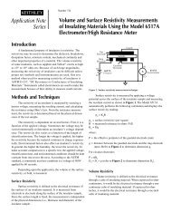
Instruction manual (155K PDF file) - Four Point Probes
Instruction manual (155K PDF file) - Four Point Probes
Instruction manual (155K PDF file) - Four Point Probes

Create successful ePaper yourself
Turn your PDF publications into a flip-book with our unique Google optimized e-Paper software.
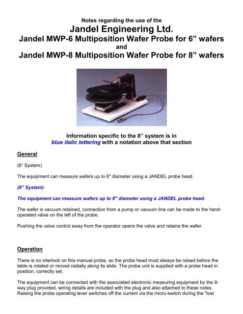
Notes regarding the use of the<br />
Jandel Engineering Ltd.<br />
Jandel MWP-6 Multiposition Wafer Probe for 6” wafers<br />
and<br />
Jandel MWP-8 Multiposition Wafer Probe for 8” wafers<br />
General<br />
(6” System)<br />
Information specific to the 8” system is in<br />
blue italic lettering with a notation above that section<br />
The equipment can measure wafers up to 6" diameter using a JANDEL probe head.<br />
(8” System)<br />
The equipment can measure wafers up to 8" diameter using a JANDEL probe head.<br />
The wafer is vacuum retained, connection from a pump or vacuum line can be made to the handoperated<br />
valve on the left of the probe.<br />
Pushing the valve control away from the operator opens the valve and retains the wafer.<br />
Operation<br />
There is no interlock on this <strong>manual</strong> probe, so the probe head must always be raised before the<br />
table is rotated or moved radially along its slide. The probe unit is supplied with a probe head in<br />
position, correctly set.<br />
The equipment can be connected with the associated electronic measuring equipment by the 9-<br />
way plug provided, wiring details are included with the plug and also attached to these notes.<br />
Raising the probe operating lever switches off the current via the micro-switch during the "lost
motion" and then raises the probe head mounting slide, so that the wafer can be loaded, after<br />
pulling the table towards the operator, to the limit of its travel. The table has a "tweezer notch" for<br />
convenience of centring the wafer relative to the rings on the table.<br />
Measurement at Wafer Center<br />
The table should be pushed to the limit of its travel away from the operator - at this position the<br />
centre of the wafer is immediately below the probe points and if the operating lever is lowered fully,<br />
the needles make contact with the wafer, and are fully compressed while the micro-switch switches<br />
the current on. Measurement can thus be made at the centre. The operating lever should then be<br />
raised so that the wafer can be removed, or measurements made at other radial positions.<br />
(6” System)<br />
Measurement at Radial Settings<br />
On the right hand side of the moving table slide are seven screws which blank off holes at 15, 20,<br />
25, 30, 35, 50 and 60mm from the "central" position. Any one, or all screws, can be removed so<br />
that the slide can be set at the appropriate radial distance dependent on the wafer diameter. There<br />
are four radial settings at 90° intervals denoted on the rotating table by "click" position, so that by<br />
raising and lowering the operating lever at each 90° position, four measurements can be made at<br />
any set radial distance.<br />
(8” System)<br />
Measurement at Radial Settings<br />
On the right hand side of the moving table slide are seven screws which blank off holes at<br />
32, 38, 50, 57, 68, and 94mm from the "central" position.<br />
Wafer ½ R 6mm from edge<br />
5" 32mm 57mm<br />
6" 38mm 68mm<br />
8" 50mm 94mm<br />
(ASTM F81-89 Sampling plan C)<br />
Any one, or all screws, can be removed so that the slide can be set at the appropriate radial<br />
distance dependent on the wafer diameter. There are four radial settings at 90° intervals denoted<br />
on the rotating table by "click" position, so that by raising and lowering the operating lever at each<br />
90° position, four measurements can be made at any set radial distance.<br />
Adjustments
1. The operating lever should be sufficiently stiff in its functioning to hold the probe head fully<br />
raised. Adjust the socket set screw in the probe head support immediately above the operating<br />
lever shaft, clockwise makes the operation more stiff.<br />
2. Check that when the lever is pulled fully down the micro-switch has operated. The probe<br />
needles should make contact with the wafer before the switch operates, if in doubt proceed as for:<br />
Exchanging Probe Head<br />
1. Remove the probe head by slackening the red clamp screw on the left hand side of the probe<br />
head mounting, lift out the probe head, unplug the lead.<br />
2. Check the micro-switch setting by pulling down the operating lever so that the slide is fully down,<br />
observe that the micro-switch has just operated, if not, correct by adjusting the screw and locking<br />
it.<br />
3. Fit a probe head into the mounting, ensuring that the bellows slide up the probe head body.<br />
Rotate the probe head so that the needles lie parallel to the front face of the mounting (use the two<br />
screws in the probe head as a guide). Position a wafer on the table because its thickness is<br />
significant. Pull down the operating handle completely, and then push the probe head down on the<br />
wafer until the insulating pad lies on the wafer surface, i.e. the needles are fully compressed, then<br />
clamp the probe head firmly with the red clamp screw, do not tighten excessively. Ensure that the<br />
micro-switch has just operated. This can be observed by slackening the adjusting screw<br />
completely until the switch is obviously not operative, then screw the screw clockwise (down) until<br />
the switch clicks. Lock the screw with the hexagon nut. RECHECK.<br />
Note that the range of thicknesses that can be accommodated is at least 0 - 1.5mm. The extra<br />
movement of the micro-switch actuator when measuring thinner wafers is absorbed by flexing of<br />
the leaf spring.<br />
Verify, once more, the setting of the micro-switch, the alignment of the probe needles, position of<br />
bellows, etc. Remove the test wafer.<br />
NB<br />
The probe head can normally be positioned with no wafer on the table, the micro-switch has<br />
already been set so that it will function correctly for wafers or specimens up to 1.5mm thick. BE<br />
CAREFUL THAT THE PROBE HEAD NEEDLES DO NOT ENTER A GROOVE OR THE<br />
CENTRAL HOLE IN THE TABLE.<br />
To Remove Light Shield from Multiposition Probe<br />
Slacken clamp screw on left hand side of probe head mounting block. Unplug the probe head and pull it out<br />
from the plastic bellows.<br />
Slacken and remove the two 6BA cheesehead screws which are holding the hinge to the column. (The right<br />
hand screw also earths the screen)<br />
Pull the screen forward and remove the two 8BA socket cap screws which secure the lower end of the lifting<br />
linkage to the screen. Access to the screws is best through the probe head mounting block using the long<br />
end of the key.
Remove the screen and also unhook the small block from the linkage.<br />
Note that the link chain can be left to hang, or taped to the underside of the column.<br />
To Replace Light Shield<br />
Reverse 1 - 5 above.<br />
P.T.F.E. No. on 9-way P.V.C.<br />
White 9 Blue<br />
Green 8 Green<br />
Red 7 Yellow<br />
Black 6 Red<br />
Screen 5 Screen<br />
1.<br />
Lemo with P.V.C. with P.T.F.E.<br />
1 Blue White<br />
2 Green Green<br />
3 Yellow Red<br />
4 Red Black<br />
5 Screen Screen<br />
Choice of Probe Head<br />
Nearly all 4-point measurements are made using a probe head which may be of various shapes and sizes,<br />
but all comprising four pointed probes spring loaded and electrically connected to the electronic equipment<br />
which supplies a constant DC measuring current and displays the measured output voltage. JANDEL probe<br />
heads offer very high precision needle spacing (±10µ) or a special execution (±5µ), checked on an<br />
interferometer microscope. The probes are precision ground tungsten carbide with 45º included angle tips<br />
and polished tip radii optically checked from 12.5 to 500 microns. The spring loading is checked<br />
electronically and can be from 10g to 250g preset. Spacings can be from 0.5mm to 1.59mm in a linear or<br />
square array. The needle guidance is by precision ruby jewel bearings at two levels.
The choice of probe head characteristics is dependent on the material to be probed. Note the following four<br />
point selection guide refers to the various possibilities, and the published ASTM Standards and<br />
recommendations can be used as a guide. Most materials can be probed with the three basic sets of<br />
characteristics viz. 1.00mm spacing, 25 micron tip radius, 100g load linear can be used to measure<br />
homogenous wafers (substrates), epitaxial layers, diffused layers, silicon on sapphire metallic films<br />
OR<br />
1.00mm spacing, 100 micron tip radius, 100g load linear for medium and high dose ion-implanted wafers,<br />
metallic films.<br />
For low dose ion implants and shallow junctions it may be necessary to use tip radii between 200 and 500<br />
microns.<br />
Conditioning<br />
All JANDEL probe head needles with a radius of greater than 25 microns are polished to an optical finish. In<br />
some situations the smooth finish does not furnish the best possible contact, so 'conditioning' may be<br />
necessary. This is effected by raising and lowering the mounted probe head on to a ceramic plate a number<br />
of times. This process produces both a cleansing action and creates microscopic asperities to promote<br />
good electrical contact with less noise without excessive penetration.<br />
Sophisticated Resistivity Mapping Systems often incorporate software programmes to determine the<br />
standard deviation of a group of measurements on a representative wafer. In this way the enhancement of<br />
the probe head performance by conditioning can be studied and the appropriate programme of conditioning<br />
undertaken.<br />
Notes on <strong>Four</strong> <strong>Point</strong> Resistivity Measuring With Jandel Equipment<br />
General<br />
Before attempting measurement one needs to know something of the sample or the wafer - is it<br />
silicon (Germanium is easier to contact and measure). Metallic and other layers are also<br />
deposited on semiconductor, sapphire or ceramic wafers.<br />
First, is the sample clean and fresh<br />
If the sample is old it may be etched, washed and dried which will remove oxide that can impede<br />
ohmic contact.<br />
Secondly, is the sample homogenous i.e. is it uniformly doped or does it have a layer on its surface<br />
e.g. by epitaxy, diffusion, ion-implantation, or sputtering etc<br />
If the sample has a layer it must be of the opposite conductivity type to the substrate i.e. electrically<br />
insulated from the substrate. A layer of the same conductivity type cannot be measured by the four<br />
point method because the substrate offers an easier path for the current, and the measured<br />
resistivity is effectively that of the substrate.<br />
If the layer is thin, meaning sub-micron, one must avoid puncturing the layer by excessive needle<br />
loading, by sharp or rough needle tips, or too rapid descent velocity of the probes, excessive<br />
current can also inject minority carriers.
All these effects cause some leakage into the substrate, so that the measuring current in the layer<br />
is reduced, and the resistivity measured is too low.<br />
Limits of Measurement Capability<br />
1. The material must be capable of being probed, i.e. the probes must be able to make ohmic<br />
contact with the material e.g. Germanium, Silicon and metals. Materials such as Gallium Arsenide<br />
cannot normally be probed unless it is doped and measured with special measuring techniques<br />
such as that in the <strong>Four</strong> Dimensions Inc. GaAs probe.<br />
2. Very low resistivity material e.g. aluminium, gold, platinum may require the maximum current<br />
from the current source to achieve a readng on the digital voltage display.<br />
Calculation of Resistivity<br />
A selection of correction factors are published by various authorities, covering the modifications to<br />
be made according to the specimen size and shape being measured, we show two examples for<br />
measurement of circular samples in the centre with a linear probe of spacing 's'.<br />
Basically, bulk resistivity (for a semi-infinite volume) = 2 x pi x s x (V/I) ohm.cm where s is the<br />
spacing of the probe in cm, I the test current, and V the measured voltage.<br />
Sheet resistance for wafers and films R S = 4.532 x V / I ohms per square.<br />
Bulk resistivity for wafers and films q = R S x t = 4.532 x V x t / I where t is the thickness in cm.<br />
General Comments<br />
1. Most wafers and films approximate to 'infinite sheets' at the present time, but if the thickness is<br />
greater than 5% of the probe spacing (normally 1.00mm) i.e. 5mm then the semi-infinite solid<br />
formula is within less than 1%.<br />
2. From the other point of view a reasonable sized wafer may be measured with a four point probe<br />
using the above sheet resistance formula. Provided the wafer thickness does not exceed 0.625 of<br />
the probe spacing the calculation is within 1%.<br />
Please see table below.
FPP Correction Factors for Sample<br />
Thickness t<br />
FPP Correction Factors for sample<br />
diameter d<br />
t/s C 1 (t/s) d/s C 2 (d/s)<br />
0.3 1.0000 10 4.1712<br />
0.4 0.9995 20 4.4364<br />
0.5 0.9974 30 4.4892<br />
0.6 0.9919 40 4.5080<br />
0.7 0.9816 50 4.5167<br />
0.8 0.9662 60 4.5215<br />
0.9 0.9459 70 4.5244<br />
1.0 0.9215 80 4.5262<br />
1.2 0.8643 90 4.5275<br />
1.4 0.8026 100 4.5284<br />
1.6 0.7419 200 4.5314<br />
1.8 0.6852 4.5320<br />
2.0 0.6337<br />
3. Remember that other geometrical effects affect the result if the wafer is not measured at the<br />
centre because the number of possible current paths is limited.<br />
We recommend study of the following original papers:<br />
a) Linear Array <strong>Probes</strong><br />
Circular wafers at centre:<br />
1. D. E. Vaughan, Br.J. Appl. Phys., 12, 414 (1961)<br />
2. M. A. Logan, Bell Sys. Tech. J., 40, 885 (1961) Off centre but on radius:<br />
3. L. J. Swartzendruber, National Bureau of Standards Technical Note 199 (1964) Perpendicular to<br />
radius:<br />
4. M. P. Albert and J. F. Combs, IEEE Trans. Electron Devices, ED-11, 148 (1964)<br />
5. L. J. Swartzendruber, Solid State Electronics, 7, 413 (1964)<br />
Rectangular sample at centre and off centre:<br />
6. M. A. Logan, Bell Sys. Tech. J., 46, 2277 (1967)<br />
Half cylinder:<br />
7. E. B. Hansen, Appl. Sci. Res., 8B, 93 (1960)<br />
Circular rod:<br />
8. H. H. Gegenwarth, Solid State Electronics, 11, 787 (1968)<br />
Rectangular bar:<br />
9. A. Marcus and J. J. Oberly, IEEE Trans. Electron. Devices, ED-3, 161 (1956)<br />
Note: All the foregoing is based on measurement using a four point linear probe, the current being<br />
passed between the outer probes and the voltage measured across the inner two probes.
) Square Array <strong>Probes</strong><br />
Small slice at centre:<br />
as 9 above<br />
Small slice along a radius:<br />
as 3 above<br />
Square sample:<br />
10. M. G. Buehler, Solid State Electronics, 10, 801 (1967)<br />
Thick sample near boundary:<br />
11. S. B. Catalano, IEEE Trans. Electron. Devices, ED-10, 185 (1963)<br />
thin infinite sheet:<br />
as 10 above<br />
Note: Square array probes have the current passed between two adjacent probes and the voltage<br />
measured across the two opposite when used for resistivity measurement. The voltage signal for a<br />
square array probe head is 50% of a linear probe head.