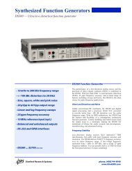
DS335 Synthesized Function Generator
DS335 Synthesized Function Generator
DS335 Synthesized Function Generator

You also want an ePaper? Increase the reach of your titles
YUMPU automatically turns print PDFs into web optimized ePapers that Google loves.
5-6 Circuitry<br />
<strong>Function</strong> Selection (<strong>DS335</strong>M6)<br />
The DPDT relay (U603, an HS212) selects between the filtered (and perhaps attenuated) waveform DAC<br />
output, and the output of the square wave generator. If the square wave output is not being used, then the<br />
square wave amplitude will be set to zero (SW_AMPL=-5 Vdc) so as to reduce crosstalk in the function select<br />
relay. The selected function is passed to the differential output amplifier.<br />
Output Amplifier (<strong>DS335</strong>M7)<br />
The output amplifier is a high speed, low distortion, discrete transistor differential amplifier. The gain is x-10<br />
for the inverting input, and x12 for the non-inverting input, and the 3 dB bandwidth is 35 MHz, it has a phase<br />
linear response to about 175 MHz, and a THD of about 0.05% to 50 kHz. The amplifier has a very low offset<br />
drift, as its dc characteristics are stabilized by an external compensated op-amp.<br />
The amplifier has a very symmetric design. This, together with it class A operation and high open loop<br />
bandwidth, keeps it distortion very low. In this circuit description, only the 'top-half' will be described, as the<br />
'bottom-half' of the amplifier operates in a completely symmetrical and complimentary manner.<br />
The signal is applied to the input differential pair (Q701 and Q702, 2N5770's). The input pair run in a constant<br />
current configuration, with the constant current source (Q706 with R741 and D701). The pnp transistor (Q700)<br />
provides an ac current to absorb the feedback current from R705. Since the input differential pair runs at<br />
constant current, independent of the input signal, their base-emitter voltages are constant, and so are not a<br />
source of distortion.<br />
To understand the operation of the amplifier, consider events when a positive input signal is applied. The<br />
base of Q701 goes up, while Q702's base goes down. This increases Q701's collector current, pulling down<br />
the base of the emitter follower, Q709, which pulls the base of Q710 and Q711 down, increasing their<br />
collector currents. This current will cause the collector voltage of Q710 to slew very quickly, and with lots of<br />
gain, because the collector load is a very high impedance. The Darlington pair, Q712 and Q713, buffer this<br />
node to drive the output, which is a 100 Ohm load. The current imbalance at the high impedance node will<br />
cause the output to continue to slew until the feedback current (though R703 and R747) brings the input<br />
differential pair back into balance.<br />
The ac gain is adjusted by setting R703. The ac gain is adjusted to match the dc gain (which is controlled by<br />
the op-amp and its feedback resistor network.) The ac gain is determined by the ratio of the feedback<br />
resistors to the emitter resistors.<br />
The op-amp (U700, a CA3140) and its feedback resistors (R700,701,702 and R723) stabilize the dc<br />
characteristics. The op-amp is externally compensated so that it will only correct low frequency errors, and so<br />
will not affect high frequency performance. The output of U700 is buffered (for extra current drive) by U701A<br />
and U701B.<br />
Output Attenuator (<strong>DS335</strong>M8)<br />
The output attenuator is a relay controlled, 50 Ohm attenuator, which allows attenuation in a binary sequence<br />
of 2 dB steps. When the power is removed (or on RESET) all of the attenuators are switched 'in'. The relays<br />
are controlled by bits written to the 8 bit latch, U800, a 74HC273. Outputs from the latch are buffered by npn<br />
emitter followers (U801, a CA3082), which drive the relay coils. Each 2 dB attenuator can reduce the output<br />
by a factor of 0.794. Output levels between these steps are obtained by adjusting the reference level to the<br />
waveform DAC. The total attenuation is 30 dB, or a factor of 0.0316, which will reduce the 7.94 Vpp level from<br />
the output amplifier to 0.25 Vpp. For ac levels below this, the pre-attenuator will be used (Sheet FG6) to<br />
provide up to 14 dB additional attenuation (for levels down to 50 mVpp).<br />
<strong>DS335</strong> <strong>Synthesized</strong> <strong>Function</strong> <strong>Generator</strong>