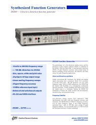
DS335 Synthesized Function Generator
DS335 Synthesized Function Generator
DS335 Synthesized Function Generator

You also want an ePaper? Increase the reach of your titles
YUMPU automatically turns print PDFs into web optimized ePapers that Google loves.
5-4 Circuitry<br />
To set an output frequency, Fout, the PIR is set to:<br />
PIR = Fout x 2^48 / Fclk<br />
where Fclk is the 10 MHz ASIC clock. Math operations to compute the PIR must be done to 48 bit precision,<br />
so, a 48x48 bit multiply is required to compute a PIR value.<br />
The ASIC registers are loaded by providing an op-code ( which tells which and how many registers to load )<br />
and data ( which is loaded into the target registers ). These op-codes and data may be provided directly by<br />
the CPU after a -HOST_REQ is issued and a HOST_ACK received. Or, a series of op-codes and data may<br />
be stored in the 32K x 8 modulation RAM (U400, a 62256). The modulation RAM is used to store data for<br />
frequency sweeps. Sweeps can consist of up to 4000 different frequencies together with amplitude leveling<br />
data.<br />
The modulation RAM is addressed by the ASIC. To load modulation op-codes and data, the start address for<br />
the modulation program is written to the ASIC's MODSTRT registers, and loaded into the modulation address<br />
counters. Op-codes and data are written sequentially to the modulation RAM as outputs to -MOD_RAM port.<br />
The -MOD_RAM port strobe writes data to the modulation RAM and increments the modulation address.<br />
There is one eight-bit DAC which is loaded as if it were an ASIC register. The DAC (U402, a AD7524)<br />
controls the reference voltage to the waveform DAC, and so the output amplitude. DAC values from 0 to 255<br />
control the reference from minus 0.75 to minus 1.25 Vdc. This DAC is used to level the output amplitude<br />
during frequency sweeps.<br />
There is a 74HC273 (U413) that is also loaded as if it were an ASIC register; its output goes directly to the<br />
SWEEP/FSK rear panel BNC. When the <strong>DS335</strong> is performing a sweep, this output provides a pulse that is<br />
synchronous with the sweep rate. When the <strong>DS335</strong> is performing internal FSK, the SWEEP/FSK ouptut<br />
voltage toggles at the FSK rate.<br />
The waveform addresses generated by the ASIC access one of four 8k long tables in waveform ROMs (U409,<br />
U411). These tables contain sine, ramp, saw and noise data. The tables are selected by the two MSB’s of the<br />
ASIC_CTL latch, (U404, a 74HC273). Data from the ROMs is latched into two 8-bit latches (U410 and U412,<br />
74F374's).<br />
Waveform DAC (<strong>DS335</strong>M5)<br />
Latched waveform data (WD0 to WD11) is filtered by 470 Ohm resistor networks before being latched into the<br />
12-bit waveform DAC (U500, a TDC1012) by the rising edge of the 10 MHz CONV clock. The differential<br />
current outputs from the DAC have a range from 0 to -40 mA:<br />
Value +OUT -OUT<br />
0 0 -40.000 mA<br />
1 -.01 -39.990<br />
7FF -19.995 -20.005<br />
800 -20.005 -19.995<br />
FFE -39.990 -00.010<br />
FFF -40.000 0<br />
Because the DAC outputs can only sink current, part of the output termination network is connected to a<br />
positive voltage source which tracks the DAC reference input. This arrangement keeps both outputs centered<br />
on 0 Vdc. This improves the performance of the DAC and eliminates any dc current from the output filters.<br />
<strong>DS335</strong> <strong>Synthesized</strong> <strong>Function</strong> <strong>Generator</strong>