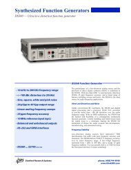
DS335 Synthesized Function Generator
DS335 Synthesized Function Generator
DS335 Synthesized Function Generator

You also want an ePaper? Increase the reach of your titles
YUMPU automatically turns print PDFs into web optimized ePapers that Google loves.
Introduction 2-1<br />
Introduction to Direct Digital Synthesis<br />
Introduction<br />
Traditional <strong>Generator</strong>s<br />
DDS<br />
Direct Digital Synthesis (DDS) is a method of generating very pure<br />
waveforms with extraordinary frequency resolution, low frequency switching<br />
time, crystal clock-like phase noise, and flexible sweeping capabilities. As an<br />
introduction to DDS let's review how traditional function generators work.<br />
Frequency synthesized function generators typically use a phase-locked loop<br />
(PLL) to lock an oscillator to a stable reference. Wave-shaping circuits are<br />
used to produce the desired function. It is difficult to make a very high<br />
resolution PLL so the frequency resolution is usually limited to about 1:10 6<br />
(some sophisticated fractional-N PLLs do have much higher resolution). Due<br />
to the action of the PLL loop filter, these synthesizers typically have poor<br />
phase jitter and frequency switching response. In addition, a separate waveshaping<br />
circuit is needed for each type of waveform desired, and these often<br />
produce large amounts of waveform distortion.<br />
DDS works by generating addresses to a waveform ROM to produce data for<br />
a DAC. However, unlike earlier techniques, the clock is a fixed frequency<br />
reference. Instead of using a counter to generate addresses, an adder is<br />
used. On each clock cycle, the contents of a Phase Increment Register are<br />
added to the contents of the Phase Accumulator. The Phase Accumulator<br />
output is the address to the waveform ROM (see diagram below). By<br />
changing the Phase Increment the number of clock cycles needed to step<br />
through the entire waveform ROM changes, thus changing the output<br />
frequency.<br />
Frequency changes now can be accomplished phase continuously in only<br />
one clock cycle. And the fixed clock eliminates phase jitter, requiring only a<br />
simple fixed frequency anti-aliasing filter at the output.<br />
The <strong>DS335</strong> uses a custom Application Specific Integrated Circuit (ASIC) to<br />
implement the address generation in a single component. The frequency<br />
resolution is equal to the resolution with which the Phase Increment can be<br />
set. In the <strong>DS335</strong>, the phase registers are 48 bits long, resulting in an<br />
impressive 1:10 14 frequency resolution. The ASIC also contains a modulation<br />
control CPU that operates on the Phase Accumulator, Phase Increment, and<br />
external circuitry to allow digital synthesis and control of waveform sweeps.<br />
The Modulation CPU uses data stored in the Modulation RAM to produce<br />
frequency sweeps. All modulation parameters, such as rate, and frequency<br />
deviation, are digitally programmed.<br />
Figure 1:<br />
Block diagram of SRS<br />
DDS ASIC<br />
<strong>DS335</strong> <strong>Synthesized</strong> <strong>Function</strong> <strong>Generator</strong>