Microchip Manufacturing
Microchip Manufacturing
Microchip Manufacturing

You also want an ePaper? Increase the reach of your titles
YUMPU automatically turns print PDFs into web optimized ePapers that Google loves.
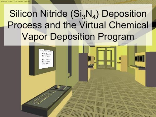
Silicon Nitride (Si 3 N 4 ) Deposition<br />
Process and the Virtual Chemical<br />
Vapor Deposition Program
Chemical Vapor Deposition A Closer Look: Si 3 N 4<br />
Overall Reaction:<br />
3 SiCl 2 H 2 (g) + 10 NH 3 (g) Si 3 N 4 (s)<br />
Dichlorosilane<br />
(DCS)<br />
Ammonia<br />
Silicon<br />
nitride<br />
+<br />
6 NH 4 Cl (g) +<br />
Ammonium chloride<br />
6 H 2 (g)<br />
Hydrogen<br />
NH 3 (gas)<br />
NH 4 Cl (gas)<br />
H 2 (gas) SiCl 2 H 2 (gas)<br />
Silicon<br />
nitride<br />
SiCl 2 H 2 (gas)<br />
NH 3 (gas)<br />
Graphics copy-write Pro. Milo Koretsky, Chemical Engineering Department at OSU<br />
Photo Courtesy of Silicon Run Educational Video
Chemical Vapor Deposition A Closer Look:<br />
Factors that Effect Film Thickness and Uniformity<br />
• Absolute flow rates of ammonia<br />
to DCS<br />
• Ratio of ammonia to DCS (fixed)<br />
• Temperature (5 zones)<br />
• Reaction time<br />
• Pressure (fixed)<br />
We’ll explore the results of changing<br />
some of these factors.<br />
DCS (gas)<br />
NH 3 (gas)<br />
NH 4 Cl (gas)<br />
H 2 (gas)<br />
NH 3 (gas)<br />
DCS (gas)<br />
Thickness<br />
Film<br />
Substrate
Virtual CVD Overview<br />
Choosing the Virtual CVD reactor parameters<br />
Pressure<br />
is Fixed<br />
Each run costs $
Film Thickness [A]<br />
Film Thickness [A]<br />
Measurement – Thickness & Uniformity<br />
• Film thickness is determined by the amount of material<br />
that reacts and is grown on the wafer<br />
• Uniformity describes the evenness of film thickness on<br />
the wafer<br />
45% Uniformity 100% Uniformity<br />
1000<br />
1000<br />
800<br />
600<br />
400<br />
200<br />
0<br />
-150 -50 50 150<br />
x position<br />
800<br />
600<br />
400<br />
200<br />
0<br />
-150 -50 50 150<br />
x position
Wafer #<br />
Measurement – Thickness & Uniformity<br />
• Film thickness is determined by the amount of material<br />
that reacts and is grown on the wafer<br />
• Uniformity describes the evenness of film thickness on<br />
the wafer<br />
NH 4 Cl (gas)<br />
H 2 (gas)<br />
NH 3 (gas)<br />
200<br />
150<br />
50% Overall Efficiency<br />
SiCl 2 H 2 (gas)<br />
0<br />
100<br />
50<br />
SiCl 2 H 2 (gas)<br />
NH 3 (gas)<br />
79% Overall Efficiency<br />
0 2000 4000 6000 8000 10000<br />
Thickness [A]
Measurement via Ellipsometer<br />
• The ellipsometer is used to measure the<br />
thickness and refractive index of<br />
transparent films.<br />
• It is made of a light source and polarizer<br />
on one side and a analyzer and detector<br />
on the other side.<br />
Detector<br />
Analyzing<br />
Polarizer<br />
Substrate<br />
Light Control<br />
Light Source<br />
Polarizing<br />
Sheet<br />
Analyzer &<br />
Detector<br />
Light Source,<br />
Control &<br />
Polarizing<br />
Sheet<br />
• Light from the source is polarized<br />
and reflected off the film.<br />
• The analyzer is rotated till no light<br />
passes through it.<br />
• The angle of rotation depends on the<br />
thickness of the film.
Virtual CVD Overview<br />
Choosing the locations on the wafer to measure<br />
Each measurement costs $
Virtual Chemical Vapor Deposition<br />
(VCVD) Program<br />
VCVD Program<br />
Semiconductor <strong>Manufacturing</strong> Fab<br />
Photo Courtesy of http://webmedia.national.com/gallery/06/06_rgb.jpg
Your Objectives:<br />
•Optimize “Recipe”<br />
◦high uniformity (within wafer and between wafers)<br />
◦meets a target thickness of 1000 Angstroms<br />
•Minimize Cost
Let’s Get Started<br />
•Open VCVD Program...