Three - University of Arkansas Physics Department
Three - University of Arkansas Physics Department
Three - University of Arkansas Physics Department

Create successful ePaper yourself
Turn your PDF publications into a flip-book with our unique Google optimized e-Paper software.
ELSEVIER Physica C 282-287 (1997) 683684<br />
Fabrication and characterization <strong>of</strong> vias for contacting YBa,Cu,O,-, rnultilayers<br />
J. W. Cooksey, S. Afonso, W. D. Brown, L. W. Schaper, S. S. Ang, R. K. Ulrich, G. J. Salamo, and F. T. Chan<br />
High Density Electronics Center, <strong>University</strong> <strong>of</strong> <strong>Arkansas</strong>, 600 W. 20th Street, Fayetteville, AR 72701 USA<br />
la order to connect multiple layers <strong>of</strong> high temperature superconductor (HTS) interconnects, low contact<br />
resistance vias must be used to maintain high signal propagation speeds and to minimize signal losses. In this work,<br />
40 pm via contacts through YBqCu,O,, /S~T~O,/S~OJYSZIYB~CU~O~~~ multilayers utilizing dry etching techniques<br />
and sputter deposited Au for contacting through the vias have been successfully fabricated and characterized. The<br />
vias connect two laser ablated YBqCu307, (YBCO) signal lines through thick (4-5 pm) SiO, insulating layers. This<br />
approach to making multilayer superconductor vias provides a low resistance contact between the YBCO layers<br />
while maintaining space efficiency and fabrication compatibility with the superconductor.<br />
1. INTRODUCTION<br />
Since the discovery <strong>of</strong> high temperature<br />
superconductivity (HTS), researchers have utilized<br />
their low resistance behavior in many applications.<br />
One such application is that <strong>of</strong> multichip modules<br />
(MCMs.) Unlike that <strong>of</strong> VLSI technologies where<br />
smaller feature sizes in successive generations allow<br />
interconnect lengths and power dissipation to be<br />
reduced, MCMs will not have that same luxury. As<br />
the complexity <strong>of</strong> ICs advances, pinout count per IC<br />
increases, and operating frequencies increase, MCM<br />
normal metal interconnections will have to grow in<br />
length and will not be allowed to reduce in crosssectional<br />
area. On MCM-D substrates, typical copper<br />
or aluminum interconnection dimensions are about 2<br />
challenge for attaining multiple layers <strong>of</strong> high density,<br />
high performance HTS interconnects appears to be in<br />
fabricating compact, low resistance vias.<br />
The work presented here focuses on this problem<br />
and describes a method <strong>of</strong> fabricating noble metal vias<br />
for use in an HTS MCM prototype.<br />
2. EXPERIMENTAL DETAILS AND RESULTS<br />
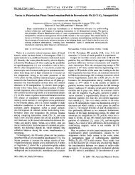
A cross-section <strong>of</strong> our multilayer YBCO structure<br />
utilizing Au vias is shown in Figure 1.<br />
Pmn PhoMbI lor VL. Ho* Etch<br />
PhoUlrL.1<br />
la UlllTlw~T~p U-r<br />
to 5 pm in thickness and between 15 and 30 pm wide ,--.<br />
with corresponding via sizes. By cooling the metal to<br />
77 K (liquid nitrogen temperature), the resistivity <strong>of</strong><br />
iuacan Im Bsh 8% U.I~SCF. PLlm. tmun-smurrwnu,<br />
copper decreases by a factor <strong>of</strong> about 7 which allows<br />
a corresponding decrease in the interconnect's crosssectional<br />
area. In order to increase the wiring density<br />
8vbb-a. 8ubeWI<br />
beyond that <strong>of</strong> cryo-cooled MCMs and improve the /. .<br />
chip-to-chip bottleneck at high frequencies,<br />
alternatives to conventional metal interconnects must<br />
be considered [I].<br />
HTS interconnections, with negligible resistivity at<br />
operating frequencies <strong>of</strong> several tens <strong>of</strong> GHz and<br />
lower, have great potential to reduce an interconnect's<br />
cross-sectional area with typical thicknesses <strong>of</strong> less<br />
than 1 pm and widths <strong>of</strong> less than 2 pm for MCM<br />
applications with similar spacings. The main<br />
0921~5~4/97/$17.00 O Elsevier Science B.V All rights re~e~ed.<br />
Pi1 S09214534(97)00495-4<br />
aub8tmw<br />
.- ._-.<br />
Figure 1. HTS via process.<br />
VaZ