Three - University of Arkansas Physics Department
Three - University of Arkansas Physics Department
Three - University of Arkansas Physics Department

You also want an ePaper? Increase the reach of your titles
YUMPU automatically turns print PDFs into web optimized ePapers that Google loves.
APPLIED PllYSICS LETTERS VOLUME 75. NUMBER 3<br />
Morphology <strong>of</strong> lnAs self-organized islands on AlAs surfaces<br />
P. ~allet,~) J. B. Smathers, and G. J. Salamob)<br />
<strong>Department</strong> <strong>of</strong> <strong>Physics</strong>, Uriiversi@ oj'drkansas, Fnyelteville, Arknrtsas 72701<br />
(Received 19 April 1999; accepted for publication 21 May 1999)<br />
We report an in situ n~olecular-bean1 epitaxy-scanning tunneling microscopy study <strong>of</strong><br />
three-dimensional (3D) sclf-organizcd lnAs islands on AlAs surfaces. The evolution <strong>of</strong> thc density<br />
and n~orphology <strong>of</strong> these islands is investigated as a function <strong>of</strong> the InAs coverage and substrate<br />
temperature. It is shown that the 2D island density is already high just prior to 3D island formation<br />
and remains constant for 3D structures as the InAs coverage is increased. This observation contrasts<br />
with the InAsJGaAs systein and makes possible the growth <strong>of</strong> very high densities <strong>of</strong> sinall quantum<br />
dots. O 1999 Anlerican Institute <strong>of</strong> <strong>Physics</strong>. [S0003-6951(99)00329-01<br />
The use <strong>of</strong> the heteroepitaxy <strong>of</strong> highly nlisn~atched inaterials<br />
to produce coherent self-assembled three-diinensional<br />
(3D) islands lying on a two-dimensional (2D) wetting layer<br />
has lead the way to a new generation <strong>of</strong> quantum functional<br />
devices.'-3 These devices are based on the extraordinary bchavior<br />
that results from carrier confinenlent in all three dimensions<br />
and are called quantum dots. Quantuin dot lasers,<br />
for example, have lower thresholds, increased modulation<br />
speed, and larger differential gain, while quanhlm dot detectors<br />
can be used at normal incidence.<br />
While the quantum dot concept sounds like there are<br />
many exciting applications, in practice, there arc some serious<br />
probleins that limit its possibilities. Onc challenge is to<br />
achieve fabrication <strong>of</strong> a large nuinber <strong>of</strong> dot structures without<br />
significant size fluctuations. Size fluctuation leads to inhon~ogeneous<br />
broadening or a shifted energy level structure<br />
for each dot, preventing formation <strong>of</strong> states that are concentrated<br />
in k space. Applications will clearly depend on the<br />
development <strong>of</strong> fabrication techniques that can control the<br />
quality, size, and uniformity <strong>of</strong> dots. For this reason, the<br />
structural characterization <strong>of</strong> self-assembled InAsIGaAs islands<br />
has been extensively pursued in the past few years.4"<br />
These investigations indicate a growth inode that is strongly<br />
depcndent on deposition conditions and interface inte~niixing.<br />
Despite the intense investigation <strong>of</strong> this system, however,<br />
many questions remain about the nature <strong>of</strong> the 2D to<br />
3D transition.<br />
While the growth <strong>of</strong> InAs islands inside a GaAs matrix<br />
has been the center <strong>of</strong> attention, careful studies have also<br />
been made in 1n~b/CJa~s,~ I~G~AS/G~AS,'~ I~G~PII~P,"<br />
~i~e/~i,'~ and 1n~sJ~l~s.l~ The InAsIAlAs quantum dots<br />
provide an especially attractive system for optical and electronic<br />
devices due to their significantly higher barrier energy.<br />
For example, the higher barrier makes possible greater tunability<br />
<strong>of</strong> the intersubband infrared transitions as well as enhanced<br />
stability at high temperatures.14<br />
In this letter, we investigate the 2D to 3D transition during<br />
the molecular-bean1 epitaxy (MBE) <strong>of</strong> InAs on AIAs. We<br />
also investigated the density and morphology <strong>of</strong> the 3D islands<br />
as a function <strong>of</strong> InAs coverage and substrate tempera-<br />
ture. We carried out our investigation using a MBE facility<br />
with an in sit11 scanning tunneling microscope (STM). Substrate<br />
ternpcratures during the growth wcre measured using<br />
an optical technique based on the wavelength dependence <strong>of</strong><br />
the band edge as a hnction <strong>of</strong> temperature. Details about the<br />
experimental apparatus can be found in Ref. 15. Samples<br />
were grown on n-type GaAs wafers. After the growth <strong>of</strong> a<br />
0.5 pm GaAs buffer layer at 580 "C, a flat GaAs surface is<br />
prcpared by annealing under an As4 flux. Thc growth <strong>of</strong><br />
AlAs is initiated at 580 OC and the substrate temperature is<br />
ramped and stabilized at 500 OC while depositing AIAs. InAs<br />
is then deposited with an As4 flux <strong>of</strong> 6.OX Torr. The<br />
growth rate is chosen to be 0.1 nionolayer per second (MLI<br />
s). We exposed the surface to both In and As fluxes during 3<br />
s following by 17 s <strong>of</strong> As only. This sequence is repeated<br />
until the desired coverage is reached. The sample is then<br />
cooled to room temperature while an As4 flux is maintained<br />
until the temperature falls below 350°C. After the sample<br />
reaches 200°C, it is transferred under vacuum to the STM<br />
chamber. Interestingly, our investigation <strong>of</strong> InAsIAlAs 3D<br />
structures shows behavior that is remarkably different from<br />
that <strong>of</strong> InAsIGaAs 3D structures, despite the fact that both<br />
AlAs and GaAs have the same lattice mismatch <strong>of</strong> 7% with<br />
InAs. This difference begins with the nature <strong>of</strong> the wetting<br />
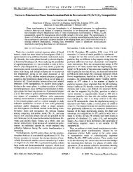
layer. Figure l(a) shows STM images <strong>of</strong> the InAs wetting<br />
layer on GaAs after the deposition <strong>of</strong> 2.1 MLs at 500 OC. The<br />
"meandering chains" indicate a highly cormgatcd surfacc<br />
due to intennixing between indium and galliurn atoms.'"<br />
Meanwhile, under the exact same conditions, STM images<br />
")~lcch.onic mail: pbalIct@comp.uark.edu<br />
b'~lectronic ruarl: sala~no(~comp.uaik.edu<br />
FIG. I. High-resolution 35X 35 nm STM imagcs <strong>of</strong> 2.1 ML <strong>of</strong> I ds dcpositcd<br />
on (a) GaAs and (b) A1As. Thc whitc rcgions on both imagcs arc onc<br />
~nionolayer high, 2D features.<br />
0003-6951/99/75(3)/337/3/$15.00 337 0 1999 American Institute <strong>of</strong> <strong>Physics</strong><br />
Downloaded 09 Mar 2008 to 130.184.237.6. Redistribution subject to AIP Ilcense or copyright; see http://apl.aip.org/apl/copyright.jsp