Three - University of Arkansas Physics Department
Three - University of Arkansas Physics Department
Three - University of Arkansas Physics Department

You also want an ePaper? Increase the reach of your titles
YUMPU automatically turns print PDFs into web optimized ePapers that Google loves.
IEEE TRANSACTIONS ON APPLIED SUPERCONDUCTIVITY, VOL. 9, NO. 2, JUNE 1999<br />
Effect <strong>of</strong> Planarization <strong>of</strong> the Bottom Superconducting<br />
Yttrium-Barium-Copper-Oxide Layer in the Multilayer Structure<br />
W. A. Luo, H. 1. Yao, S. Afonso, S. I. Qin*, S. H. Yoo, S. Ang,<br />
W. D. Brown, G. J. Salamo, and F. T. Chan<br />
<strong>University</strong> <strong>of</strong> <strong>Arkansas</strong>, Fayetteville, AR 72701<br />
ABSTRACT - YBCO/YSZ/S~OZ/YSZ/YBCO multi-layer<br />
structures have been successful~y grown on single crystal YSZ<br />
substrates. The YBCO superconducting layers (300 nm thick)<br />
were deposited using pulsed laser deposition (PLD). The YSZ<br />
layers (300 nm thick) which are biaxially aligned were deposited<br />
using PLD and the ion beam assisted deposition (IBAD). A<br />
thick silicon dioxide layer (2-4 microns) was sandwiched<br />
between the YSZ layers to meet the low dielectric constant<br />
requirement for multi-chip module applications. However, if the<br />
bottom superconducting layer was patterned into<br />
interconnecting lines as required in device applications, the<br />
surface <strong>of</strong> the YSZISiO2NSZ on top <strong>of</strong> the patterned bottom<br />
superconducting layer had a roughness <strong>of</strong> about 500 nm. As a<br />
result, the top YBCO was no longer superconducting. Thus,<br />
planarization <strong>of</strong> the patterned bottom superconducting layer<br />
becomes a key issue. We have developed a "fill-in and lift-<strong>of</strong>f'<br />
process to fill the gap between the patterned bottom<br />
superconducting lines with YSZ. As a result, we were able to<br />
reduce the surface roughness <strong>of</strong> the bottom YBCO layer to<br />
about 10 nm so the top layer was superconducting with a critical<br />
temperature <strong>of</strong> 87 K.<br />
One potential application <strong>of</strong> high temperature<br />
superconducting (HTS) films is for signal interconnects<br />
between integrated circuit chips on a muki-chip module<br />
(MCM) substrate. A typical HTS MCM needs at least four<br />
layers: power plane, ground plane, and two or more signal<br />
planes [I]. Using a new approach, called the Interconnected<br />
Mesh Power System (IMPS) 121, a superconducting MCM<br />
can be realized with only two superconducting layers. This<br />
reduction makes the JMPS approach to fabricating a<br />
superconducting MCM very attractive since it significantly<br />
reduces material and technological demands as well as cost.<br />
Even with only two superconducting layers required,<br />
however, several problems have prevented the realization <strong>of</strong><br />
a practical MCM. For example, using Yttrium-Barium-<br />
Copper-Oxide (YBCO) as the superconducting material, S.<br />
Afonso et al. have successfully fabricated YBCONSZI<br />
Si0,IYSZNBCO multi- layer structures [3]. In order to<br />
keep the distributed capacitance low, a thick SiO, layer (1-<br />
2pm) whose dielectric constant is less than four was chosen<br />
to isolate the two superconducting interconnects, and h o<br />
biaxially aligned Yttrium Stabilized Zirconia (J'SZ) layers<br />
were deposited on top and underneath the SiO, as buffer<br />
layers to prevent diffusion <strong>of</strong> the amorphous SiO, into the<br />
YBCO layers. However, when the bottom YBCO layer is<br />
patterned into interconnecting lines, the surfilce <strong>of</strong> the<br />
YSZ/SiO,/YSZ is no longer flat. The rough~less <strong>of</strong> the<br />
surface is usually greater than the thickness <strong>of</strong> the bottom<br />
YBCO layer due to over etching in the patterning process.<br />
Since the top YBCO layer is found not to be superconducting<br />
when fabricated on a rough surface, the planarization <strong>of</strong> such<br />
a rough surface becomes a key issue. In this paper we report<br />
on a "fill-in and lift-<strong>of</strong>f" planarization procedure and the<br />
effect <strong>of</strong> planarization <strong>of</strong> the bottom superconducting YBCO<br />
layer on the performance <strong>of</strong> the top YHCO layzr<br />
superconducting layer in the multi-layer structure.<br />
JJ. EXPERIMENTAL DETAILS AND RESULTS<br />
A. Patterned Multilayer Structure<br />
We fabricated a YBCO/YSZ/SiO,NSZNBCOIYSZ<br />
(substrate) multi-layer structure via a procedure described in<br />
[3]. Both the top and bottom YBCO layers were patterned<br />
into meander lines which were 19 cm long. The line widths<br />
<strong>of</strong> the bottom and top YBCO interconnect lines were 2011m<br />
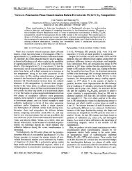
and 30pm, respectively, as shown in Fig. 1. The resistance<br />
Manuscript received September 15, 1-998.<br />
This work was supported in part by DARPA (Contract No. 972-93-1- (a) Bottom YBCO pattern (b) Top YBCO pattern<br />
0036) Ulrough HiDEC at the <strong>University</strong> <strong>of</strong> <strong>Arkansas</strong>, U.S. Army research<br />
Office DAAH04-96-1-0455, and NSF DMR 9318946. Fig. I. Schematic diagram <strong>of</strong> the meander line patterns in<br />
*Permanent address: Guizhou <strong>University</strong>, Guiyang 550025, P. R. China, YBCONSWSiO,NSZNBCO multi-layers: (a) bottm YBCO; (b) top<br />
Work partially supported by the Science and Technology Council <strong>of</strong> YBCO. (The diagram is not drawn to scale, line widths in (a) and (b) are<br />
Guizhou Province. P. R. China.<br />
2Ovm and 30um respectively, each 19 cm long).