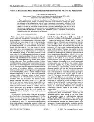
Three - University of Arkansas Physics Department
Three - University of Arkansas Physics Department
Three - University of Arkansas Physics Department

You also want an ePaper? Increase the reach of your titles
YUMPU automatically turns print PDFs into web optimized ePapers that Google loves.
Proceedings <strong>of</strong> SPIE - v 4217, p 235-238,2002<br />
2000 International Conference on High-Density Interconnect and Systems packaging<br />
Creating Optical Interconnects in Strontium Barium Niobate<br />
Matthew Klotz and Gregory J. Salamo<br />
<strong>Physics</strong> <strong>Department</strong>. <strong>University</strong> <strong>of</strong> <strong>Arkansas</strong>, Fayetteville, AR 7270 1<br />
(501) 575-2506<br />
salarno@comp.uark.edu<br />
Mordechai Segev<br />
<strong>Department</strong> <strong>of</strong> Electrical Engineering and Center for Photonics and Opto-Electronic<br />
Materials (POEM), Princeton <strong>University</strong>, Princeton, New Jersey 08544<br />
segev@ee.princeton.edu<br />
ABSTRACT<br />
In this paper we report on the use <strong>of</strong> soliton formation to create permanent waveguides by selectively reorienting<br />
ferroelectric domains within the propagating light beam. For the experiment, the output <strong>of</strong> an argon-ion laser is<br />
collimated andfocused to a spot size <strong>of</strong> I2 pm on the front face <strong>of</strong> a I cm cubic SBN:75 crystal. When a 3 kV/cm<br />
electric field is applied to the crystal along the direction <strong>of</strong>the spontaneous polarization. the beam selffocuses 10 its<br />
input diameter. The externalfield is then removed and a unifarm background beam that fills the crystal is swilched<br />
on. The space charge field due to photoinduced screening charges is larger than the coercive field <strong>of</strong>' the<br />
ferroelectric domains and causes the domains in the area <strong>of</strong> the incident beam to reverse their orientation. At<br />
equilibrium, a new space charge field, due to the bound charge at the domain boundaries is locked in place. This<br />
new field increases the index <strong>of</strong> refraction in only the area <strong>of</strong>the original soliton, so that a waveguide is formed<br />
The waveguides are observed to have the same size as the original soliton, exhibit single mode behavior and last<br />
indeI;nirely.<br />
In oddition to crealing single and multiple waveguides, a coherent collision <strong>of</strong> two solitons was used 10<br />
create several y-junctions in the crystal. Two mutually coherent, in phase beams were focused on the entrance face<br />
<strong>of</strong>the crystal with a peak to peak separation <strong>of</strong>33 pm. As the applied electric field wus increased, the two beams<br />
fused into one output beam, forming a yjunction. Following the procedure outlined above, several y-junctions were<br />
fixed in the ctystal.<br />
Key Words: Optical Interconnect, self-induced waveguides<br />
Introduction<br />
Optical spatial solitons [I] in photorefiactive crystals<br />
[2] have shown potential to form graded index<br />
waveguides which-can guide other beams [3,4]. A<br />
soliton forms when a photoinduced index change in<br />
the material exactly compensates for the difiaction <strong>of</strong><br />
the beam; i.e. the beam creates its own waveguide. In<br />
photorefiactive materials, a screening soliton is<br />
formed by the screening <strong>of</strong> an externally applied<br />
electric field through the transport <strong>of</strong> photoinduced<br />
carries [5]. The picture to the right ( Fig.l) is a top<br />
view <strong>of</strong> a photorefractive crystal showing a lop<br />
diameter incident laser beam difiacting as it<br />
propagates from the entrance face to the exit face <strong>of</strong> an<br />
unbiased crystal. Just below the difhcting picture, is a<br />
top view when the crystal is biased and the laser beam<br />
Fig.1. Top view showing an optical wire