DSP Selection Guide
DSP Selection Guide
DSP Selection Guide

Create successful ePaper yourself
Turn your PDF publications into a flip-book with our unique Google optimized e-Paper software.
System Solutions<br />
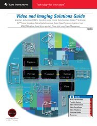
Video and Imaging<br />
35<br />
➔<br />
Power Management Products for the TMS320DM64x <strong>DSP</strong> Generation<br />
Get samples, datasheets, Evaluation Modules (EVMs) and app reports at: power.ti.com<br />
Suggested Texas Instuments Power Management Solutions for Battery-Powered TMS320DM644x/TMS320DM643x Processors<br />
Core and I/O Voltages<br />
Synchronous Non-Synchronous Synchronous Non-Synchronous PMU<br />
Input Controller Controller Integrated FET Integrated FET Multiple-Output<br />
Voltage LDO (External FETs) (External FET and Diode) Converter Converter Controller<br />
3.3 V TPS75401 TPS40041 TPS64200 TPS62040 TPS65023<br />
5 V TPS75401 TPS40042 TPS64200 TPS62040 TPS54350 TPS65023<br />
12 V TPS40190 TPS40200 TPS5420 TPS5124<br />
24 V TPS40200* TPS5420*<br />
*Due to Vout/Vin ratio core voltage may have to be stepped down from I/O voltage.<br />
I/O supply 3.3 V, current up to 1 A<br />
Core supply down to 1.0 V, current up to 2 A<br />
Suggested Texas Instuments Power Management Solutions for Line-Powered TMS320DM644x/DM643x/DM64x Processors<br />
Core and I/O Voltages<br />
Synchronous Non-Synchronous Synchronous Non-Synchronous Non-Isolated Isolated PMU<br />
Input Controller Controller Integrated FET Integrated FET Power Power Multiple-Output<br />
Voltage LDO (External FETs) (External FET and Diode) Converter Converter Module Module Controller<br />
3.3 V TPS75401 TPS40041 TPS64200 TPS54317 PTH04070 TPS65023<br />
5 V TPS75401 TPS40042 TPS40200 TPS54317 TPS54350 PTH04070 TPS65023<br />
12 V TPS40190 TPS40200 TPS54350 TPS54350 PTH08080 TPS5124<br />
24 V TPS40057 TPS40200* TPS5430* PTN78000* PTB78560*<br />
48 V TPS40061 TPS40200* PTMA403033*<br />
*Due to Vout/Vin ratio core voltage may have to be stepped down from I/O voltage.<br />
I/O supply 3.3 V, current up to 1 A<br />
Core supply down to 1.0 V, current up to 2 A<br />
V IN<br />
<strong>DSP</strong>_EN<br />
V IN<br />
10 Ω<br />
1 F<br />
V CC<br />
TPS65023<br />
4.7 kΩ<br />
4.7 kΩ<br />
DaVinci<br />
TMS320DM644x<br />
VDCDC3<br />
V IN<br />
VDCDC3<br />
EN<br />
V IN<br />
1 F<br />
4.7 F<br />
10 F<br />
10 F<br />
10 F<br />
100 kΩ<br />
1 nF<br />
100 kΩ<br />
100 kΩ<br />
VINDCDC1<br />
VINDCDC2<br />
VINDCDC3<br />
VIN_LDO<br />
LOW_BATT<br />
PWRFAIL_SNS<br />
LOWBAT_SNS<br />
HOT_RESET<br />
TRESPWRON<br />
DEFLDO1<br />
DEFLDO2<br />
LDO_EN<br />
VSYSIN<br />
VBACKUP<br />
VRTC<br />
PWRFAIL<br />
DCDC2_EN<br />
DCDC1_EN<br />
DCDC3_EN<br />
DEFDCDC3<br />
DEFDCDC2<br />
DEFDCDC1<br />
SCLK<br />
SDAT<br />
INT<br />
VDCDC1<br />
L1<br />
VDCDC2<br />
L2<br />
LDO1<br />
LDO2<br />
VDCDC3<br />
L3<br />
RESPWRON<br />
AGND1<br />
AGND2<br />
PGND1<br />
PGND2<br />
PGND3<br />
2.2 H<br />
100 kΩ<br />
2.2 H<br />
2.2 H<br />
22 F<br />
22 F<br />
2.2 F<br />
2.2 F<br />
22 F<br />
100 kΩ<br />
SCLK<br />
SDAT<br />
CVDD<strong>DSP</strong><br />
USB_VDD1P2LDO<br />
CVDD<br />
APLLREFV<br />
VDDA_1P1V<br />
DVD18<br />
DVDDR2<br />
VDDA_1P8V<br />
USB_VDD1P8<br />
M24VDD<br />
PLLVDD18<br />
DDR_VDDDL<br />
MXVDD<br />
USB_VDDA3P3<br />
DVDD33<br />
1.2-V<br />
Domain<br />
1.8-V<br />
Domain<br />
3.3-V<br />
Domain<br />
Texas Instruments 1Q 2007<br />
<strong>DSP</strong> <strong>Selection</strong> <strong>Guide</strong>