Smart Non-Default Routing for Clock Power Reduction - UCSD VLSI ...
Smart Non-Default Routing for Clock Power Reduction - UCSD VLSI ...
Smart Non-Default Routing for Clock Power Reduction - UCSD VLSI ...

Create successful ePaper yourself
Turn your PDF publications into a flip-book with our unique Google optimized e-Paper software.
<strong>Smart</strong> <strong>Non</strong>-<strong>Default</strong> <strong>Routing</strong> <strong>for</strong> <strong>Clock</strong> <strong>Power</strong> <strong>Reduction</strong><br />
Andrew B. Kahng †‡ , Seokhyeong Kang † and Hyein Lee †<br />
† ECE and ‡ CSE Departments, University of Cali<strong>for</strong>nia at San Diego<br />
abk@ucsd.edu, shkang@vlsicad.ucsd.edu, hyeinlee@ucsd.edu<br />
ABSTRACT<br />
At advanced process nodes, non-default routing rules (NDRs) are<br />
integral to clock network synthesis methodologies. NDRs apply<br />
wider wire widths and spacings to address electromigration constraints,<br />
and to reduce parasitic and delay variations.<br />
However,<br />
wider wires result in larger driven capacitance and dynamic power.<br />
In this work, we quantify the potential <strong>for</strong> capacitance and power<br />
reduction through the application of “smart” NDR (SNDR) that<br />
substitute narrower-width NDRs on selected clock network segments,<br />
while maintaining skew, slew, delay and EM reliability criteria.<br />
We propose a practical methodology to apply smart NDRs<br />
in standard clock tree synthesis flows. Our studies with a 32/28nm<br />
library and open-source benchmarks confirm substantial (average<br />
of 9.2%) clock wire capacitance reduction and an average of 4.9%<br />
clock switching power savings over the current fixed-NDR methodology,<br />
without loss of QoR in the clock distribution.<br />
Categories and Subject Descriptors<br />
B.7.2 [Hardware]: INTEGRATED CIRCUITS—Design Aids; J.6<br />
[Computer Applications]: COMPUTER-AIDED ENGINEERING<br />
General Terms<br />
Algorithms, Design, Per<strong>for</strong>mance<br />
Keywords<br />
<strong>Clock</strong> Network Synthesis, <strong>Clock</strong> Network Optimization, <strong>Power</strong> Minimization<br />
1. INTRODUCTION<br />
<strong>Clock</strong> distribution is well-known to have a large impact on integratedcircuit<br />
per<strong>for</strong>mance, area and power consumption. From the 40nm<br />
node onward, non-default routing rules (NDRs) have become an<br />
integral element of clock tree synthesis (CTS) methodology, as a<br />
means of reducing electromigration (EM) violations and delay variations.<br />
NDRs specify per-net, per-layer requirements <strong>for</strong> the router<br />
to use wiring geometries that differ from the default single-width,<br />
single-spacing (1W1S) configuration. Example NDRs might include<br />
(2W2S) (double-width, double-spacing), (1W3S), (4W2S),<br />
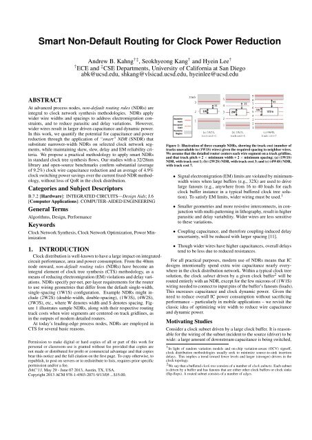
(3W3S), etc., where W denotes width and S denotes spacing. Figure<br />
1 illustrates sample NDRs, along with their respective routing<br />
track costs when wire segments are centered on track gridlines, as<br />
in the outputs of modern detailed routers.<br />
At today’s leading-edge process nodes, NDRs are employed in<br />
CTS <strong>for</strong> several basic reasons.<br />
Permission to make digital or hard copies of all or part of this work <strong>for</strong><br />
personal or classroom use is granted without fee provided that copies are<br />
not made or distributed <strong>for</strong> profit or commercial advantage and that copies<br />
bear this notice and the full citation on the first page. To copy otherwise, to<br />
republish, to post on servers or to redistribute to lists, requires prior specific<br />
permission and/or a fee.<br />
DAC’13, May 29 - June 07 2013, Austin, TX, USA.<br />
Copyright 2013 ACM 978-1-4503-2071-9/13/05 ...$15.00.<br />
Figure 1: Illustration of three example NDRs, showing the track cost (number of<br />
tracks unavailable to (1W1S) wires) given the required spacing to neighbor wires.<br />
We assume that the detailed router centers each wire segment on a track gridline,<br />
and that track pitch = 2 × minimum width = 2 × minimum spacing; (a) (1W1S)<br />
NDR, with track cost 1; (b) (2W2S) NDR, with track cost 3; and (c) (4W4S) NDR,<br />
with track cost 7.<br />
• Signal electromigration (EM) limits are violated by minimumwidth<br />
wires when large buffers (e.g., 32X) are used to drive<br />
large fanouts (e.g., anywhere from 16 to 40 loads <strong>for</strong> each<br />
clock buffer instance in a typical buffered clock tree solution).<br />
To satisfy EM limits, wider wiring must be used. 1<br />
• Smaller geometries and more resistive interconnects, in conjunction<br />
with multi-patterning in lithography, result in higher<br />
parasitic and delay variability. Wider wires are less sensitive<br />
to these variations.<br />
• Coupling capacitance, and there<strong>for</strong>e coupling-induced delay<br />
uncertainty, will be reduced with larger spacing [11].<br />
• Though wider wires have higher capacitances, overall delays<br />
tend to be less due to reduced resistances.<br />
For all practical purposes, modern use of NDRs means that IC<br />
designs intentionally spend extra wire capacitance nearly everywhere<br />
in the clock distribution network. Within a typical clock tree<br />
solution, the clock subnet driven by a given clock buffer 2 will be<br />
routed entirely with an NDR, except <strong>for</strong> the few microns of (1W1S)<br />
wiring needed to connect to input pins of the buffer’s fanouts (loads).<br />
This increases capacitance and clock dynamic power. Given the<br />
need to reduce overall IC power consumption without sacrificing<br />
per<strong>for</strong>mance – particularly in mobile applications – we revisit the<br />
classic idea of optimizing wire width to reduce wire capacitance<br />
and dynamic power.<br />
Motivating Studies<br />
Consider a clock subnet driven by a large clock buffer. It is reasonable<br />
<strong>for</strong> the wiring of the subnet incident to the source (driver) to be<br />
wide: a large amount of downstream capacitance is being switched,<br />
1 In light of random variation models and on-chip variation-aware (OCV) signoff,<br />
clock distribution methodologies usually seek to minimize source-to-sink insertion<br />
delays. This implies a trend toward fewer levels and larger (stronger) drivers in the<br />
clock topology.<br />
2 We say that a buffered clock tree consists of a number of clock subnets. Each subnet<br />
is driven by a buffer and has fanouts that are either other clock buffers or clock sinks<br />
(flip-flops). A routed subnet consists of a number of edges.
Normalized Max WL, Wire Cap (%)<br />
and this takes more time (with more current flow) with more downstream<br />
load. However, as we follow the subnet’s wiring topology<br />
away from the source, the number of downstream loads continues<br />
to decrease with every branching of the topology, until each leaf<br />
segment in the subnet’s routing tree has only one downstream load.<br />
Figure 2 summarizes statistics <strong>for</strong> 64-sink clock subnets routed by<br />
Cadence Encounter DIS V10.1 [24]. The number of downstream<br />
loads (reflecting the average current) is highest near the source<br />
(driver) buffer, but rapidly decreases <strong>for</strong> the overwhelming majority<br />
of the clock subnet wirelength. Thus, there is no (electromigrationreliability)<br />
reason <strong>for</strong> a 2W or 3W NDR to persist <strong>for</strong> the entire<br />
routing topology of a given clock subnet.<br />
ogy used to generate the figure are from a public-domain 32/28nm<br />
PDK [26]; 32X buffers are used <strong>for</strong> driver and sinks. In this case,<br />
application of the SNDR can reduce wire capacitance by 27% “<strong>for</strong><br />
free” - that is, with zero decrease in maximum driven wirelength, at<br />
r = 0.9. Alternatively, wire capacitance can be reduced by 34% at<br />
the cost of 5% decrease in maximum driven wirelength, at r = 1.0.<br />
With the above studies as our starting point, we explore the dichotomy<br />
between today’s fixed NDR methodology and a possible<br />
smart NDR methodology. The cartoon of Figure 4 shows that<br />
fixed NDRs on clock subnets result in larger driven capacitance,<br />
potentially leading to larger currents, larger drivers, and increased<br />
dynamic power. (Indeed, if the larger drivers violate signal EM<br />
limits, even the larger (wider) NDRs may be required.) By contrast,<br />
smart NDRs taper wire widths as the number of downstream loads<br />
decreases, reducing driven capacitance, dynamic power, and the<br />
number and size of buffers.<br />
larger<br />
capacitance<br />
smaller<br />
capacitance<br />
FixedNDR<br />
(wider wire)<br />
<strong>Smart</strong>NDR<br />
(tapering)<br />
fewer/smaller<br />
clock buffers, power<br />
more/larger<br />
buffers, power<br />
Figure 2: Study of 64-sink subnets routed by Cadence Encounter DIS V10.1 [24].<br />
Approximately 80% of clock subnet wirelength is in the lower levels of the tree,<br />
with few downstream loads and lower currents. The wire segment incident to the<br />
source has highest current but on average is only a small fraction of a subnet’s<br />
total wirelength.<br />
140%<br />
120%<br />
100%<br />
80%<br />
60%<br />
40%<br />
20%<br />
0%<br />
Maximum Wirelength<br />
Capacitance<br />
0 0.1 0.2 0.3 0.4 0.5 0.6 0.7 0.8 0.9 1<br />
SNDR Ratio (r = SNDR length / total length)<br />
(a)<br />
1-r<br />
r<br />
(b)<br />
3W3S<br />
1W4S<br />
Figure 3: (a) Electrical per<strong>for</strong>mance when an equivalent-pitch SNDR (1W4S)<br />
is applied to a fraction r of a wire with a given original NDR (3W3S). Shown<br />
are maximum wirelength possible while satisfying a prescribed slew constraint,<br />
and total wire capacitance (both values normalized, and plotted against the y-<br />
axis). The ratio r = 0.9 achieves 27% capacitance reduction without incurring<br />
any reduction of maximum wirelength. (b) Illustration of tapering of wire from<br />
the original NDR (blue color) to the SNDR (red color). SPICE simulation is used<br />
to determine delay and slew with different SNDR ratios r.<br />
Further motivation is obtained from SPICE experiments that evaluate<br />
the potential <strong>for</strong> SNDR-based capacitance reduction without<br />
loss of electrical per<strong>for</strong>mance. We study a symmetric H-tree [1]<br />
with a large buffer as driver, and 16 identical buffers as sinks. We<br />
sweep an SNDR ratio, r (i.e., wirelength with a given SNDR, divided<br />
by total wirelength – see Figure 3 (b)), to observe the impacts<br />
of SNDR wire tapering from different fixed original NDR widths<br />
and spacings. We assume that the signal transition at the input pin<br />
of the driver cell has 50ps slew time, and we find the maximum<br />
wirelength which maintains the same slew time at the end of the<br />
wire (i.e., at sink input pins), as well as the corresponding total wire<br />
capacitance. 3 For example, Figure 3 shows maximum wirelength<br />
under the 50ps maximum slew time constraint, and wire capacitance<br />
(both values normalized and plotted against the y-axis), when<br />
a (1W4S) SNDR is applied to save capacitance from an equivalentpitch<br />
(3W3S) original NDR. The library and interconnect technol-<br />
3 Because the H-tree is symmetric, greater wirelength means that the sinks of the H-<br />
tree are spaced farther apart.<br />
EM violations<br />
Figure 4: Intuitive dichotomy between today’s “fixed NDR” methodology and a<br />
potential “smart NDR” methodology.<br />
This Work<br />
In this work, we assess the potential <strong>for</strong> capacitance and power<br />
reductions through use of “smart” NDRs (SNDRs) that substitute<br />
narrower-width NDRs <strong>for</strong> selected clock net segments while maintaining<br />
skew, slew, delay and EM reliability criteria. We <strong>for</strong>mulate<br />
the optimal application of SNDRs <strong>for</strong> a given clock subnet as a<br />
quadratically constrained program. We also demonstrate the practicality<br />
of a flow that applies SNDRs at the end of the CTS phase<br />
in a commercial place-and-route tool.<br />
The main contributions of our work are summarized as follows.<br />
• We per<strong>for</strong>m studies of practical clock routing instances and<br />
NDRs to establish the potential <strong>for</strong> substantial dynamic power<br />
reductions using SNDRs.<br />
• We <strong>for</strong>mulate optimal application of SNDRs as a quadratically<br />
constrained program to minimize wire capacitance under<br />
skew, slew, delay and EM constraints, and we efficiently<br />
solve this problem <strong>for</strong> each subnet of a given clock tree.<br />
• We extend our SNDR solution approach to the entire clock<br />
tree by propagating skew constraints from downstream subnets<br />
to upstream subnets.<br />
• We also propose a practical flow to apply SNDRs transparently<br />
post-CTS within a standard commercial place-and-route<br />
tool.<br />
• We empirically confirm an average of 16% clock wire capacitance<br />
reduction, and 5% total clock power reduction, achieved<br />
by our proposed technique, as compared to traditional CTS<br />
approaches with fixed NDRs.<br />
The remainder of this paper is organized as follows. In Section<br />
2, we give an overview of related literature. Section 3 <strong>for</strong>mulates<br />
the SNDR problem, and Section 4 describes our wire-tapering approach.<br />
Section 5 provides experimental results and analysis. We<br />
give conclusions and ongoing research directions in Section 6.
2. RELATED WORK<br />
Wire width optimization (tapering) <strong>for</strong> clock and signal distribution<br />
has been extensively studied since the early 1990s. In this<br />
section, we survey related literature according to three main categories:<br />
(1) works on wire width optimization in clock trees; (2)<br />
electromigration-constrained wire sizing methods; and (3) coupling<br />
noise-driven wire sizing methods.<br />
(1) Wire sizing in clock trees. Many works ( [19], [9], [23], [15],<br />
[14], [17]) have applied wire sizing to minimize skew in clock<br />
trees. Tsai et al. [19] propose a dynamic programming method <strong>for</strong><br />
simultaneous buffer insertion and wire sizing to optimize delay and<br />
power of a given zero-skew or useful-skew clock tree. They calculate<br />
a feasible delay-capacitance region <strong>for</strong> all nodes in a bottomup<br />
phase, then determine buffer locations/widths and wire widths.<br />
Guthaus et al. [9] propose sequential linear programming as well<br />
as quadratic programming based clock buffer/wire sizing to minimize<br />
skew. The <strong>for</strong>mer technique uses first-order sensitivities <strong>for</strong><br />
a small region of buffer/wire size solutions to represent a nonlinear<br />
objective using a set of linear functions. Zhu et al. [23] per<strong>for</strong>m<br />
wire sizing to minimize skew using Gauss-Marquardt leastsquares<br />
minimization. Pullela et al. [15] use wire width widening<br />
to reduce clock skew, delay and process variability impact.<br />
Their method starts with a minimum-delay tree and then optimizes<br />
skew by widening wires based on a delay sensitivity to wire width<br />
derived from Elmore delay [8]. In subsequent work [17], they<br />
suggest an analytical moment-sensitivity based methodology, using<br />
the moments of the transfer function of an RC tree circuit, to<br />
simultaneously reduce skew and slew. Liu et al. [14] also propose<br />
simultaneous clock routing, wire sizing and buffer insertion based<br />
on the Deferred-Merge Embedding algorithm [2] [3].<br />
To our understanding, previous literature on clock tree wire sizing<br />
emphasizes timing optimization; exceptions are [19] and [9],<br />
the latter of which incorporates a power constraint. 4 In contrast to<br />
previous works, use of NDRs in clock routing is now largely driven<br />
by signal EM reliability limits. Moreover, previous works have<br />
various limitations such as continuous sizing that limit application<br />
within conventional physical design methodologies.<br />
(2) Electromigration-constrained wire sizing. The literature on<br />
EM-constrained wire sizing has centered on power/ground networks.<br />
Tan et al. [20] suggest sequential linear programming-based wire<br />
sizing that considers IR drop, EM and other design constraints<br />
while minimizing area. A nonlinear function of constraints is relaxed<br />
to a sequence of linear programs which always enables convergence<br />
to an optimum solution. Wu et al. [22] propose a power/<br />
ground wire sizing algorithm with IR drop, EM and minimumwidth<br />
constraints. A penalty method is used to solve the nonlinear<br />
problem so as to achieve area minimization of the power/ground<br />
network. For clock trees, Pullela et al. [16] consider an EM constraint<br />
in their low-power clock tree design methodology. They<br />
optimize a clock tree with buffer insertion by decreasing wire width<br />
while satisfying bounds on process variation-dependent skew and<br />
current density. Among all previous works of which we are aware,<br />
the work of [16] is the closest to our present target; however, buffer<br />
insertion is not our objective as it potentially draws more power and<br />
causes more EM violations in a vicious cycle (recall Figure 4).<br />
(3) Noise-driven wire sizing. Last, wire sizing has been analyzed<br />
in conjunction with spacing to address coupling noise sensitivity.<br />
Cong et al. [5] propose symmetric and asymmetric wire sizing and<br />
spacing to minimize the weighted sum of coupling capacitanceinduced<br />
delay at all sinks. Lagrangian relaxation is used to solve<br />
4 Of separate interest is the literature on wire sizing in general signal routing trees.<br />
These works are exemplified by Chen et al. [4], which targets signal routing and does<br />
not consider skew. The authors of [4] apply Lagrangian relaxation <strong>for</strong> gate and wire<br />
sizing to minimize area subject to a maximum delay bound.<br />
the same problem as in [4], but it is shown that proper wire sizing<br />
can further reduce delay when coupling capacitance is considered.<br />
In a subsequent work, Cong et al. [6] study a simultaneous wire<br />
spacing problem <strong>for</strong> multiple nets, to deal with crosstalk noise. In<br />
our methodology, although we do not address the noise problem<br />
directly, by increasing wire spacing, we reduce the coupling capacitance<br />
(and coupling-induced delay variation) as well.<br />
3. PROBLEM FORMULATION<br />
We seek to apply different NDRs (i.e., smart NDRs) to each<br />
wire segment of a given routed clock net, to reduce total wire capacitance<br />
and dynamic power subject to reliability and electrical<br />
requirements. More specifically, we want to minimize tree capacitance<br />
without violating slew, skew, clock source-to-sink insertion<br />
delay, and EM reliability constraints. Our focus is on an “isoarea”<br />
use model that is transparent to existing CTS flows: we<br />
start with a routed CTS solution, then identify a set of wire segment<br />
width reductions that save power without affecting any (skew,<br />
slew, etc.) solution metric. 5 Below, we describe such a transparent<br />
flow, which imports implemented SNDRs back into the P&R tool<br />
as DRC-clean modified DEF (Design Exchange Format, [30]) <strong>for</strong><br />
extraction and per<strong>for</strong>mance analysis, with no ECO routing needed<br />
<strong>for</strong> any other nets.<br />
Table 1 presents the notations that we use to describe our problem<br />
<strong>for</strong>mulation and algorithm. Upper bounds on slew (transition)<br />
time, skew, and insertion delay are respectively denoted by U S , U K ,<br />
and U L . We use e to indicate an edge (between clock buffers,<br />
clock sinks, or Steiner points) in the clock tree. Given a clock<br />
tree T with edges e ∈ T , a set N of allowed SNDRs (indexed as<br />
n) with maximum current limit E e,n <strong>for</strong> edge e with SNDR n ∈<br />
N, and electrical per<strong>for</strong>mance bounds U S , U K and U L , our SNDR<br />
optimization seeks to map each edge width w e to an SNDR n ∈ N<br />
while minimizing total wire capacitance, subject to the constraints<br />
E e,n , U S , U K and U L .<br />
Minimize: ∑ C e<br />
e∈T<br />
Subject to:<br />
S v ≤ U S , I e ≤ E e,we , L v ≤ U L , K u,v ≤ U K ,<br />
w e ∈ N, w e > w desc(e) , (∀v,e ∈ T ) (1)<br />
Table 1: Notation<br />
Notation<br />
Meaning<br />
C e<br />
capacitance of edge e<br />
S v<br />
slew at the node v<br />
I e<br />
average current of edge e<br />
w e<br />
NDR of edge e, w e ∈ N<br />
x e the alternative NDR variable, x e = ln(w e )<br />
D u,v<br />
delay from node u to node v<br />
K u,v<br />
skew between node u and node v<br />
L v<br />
clock latency at sink v<br />
T<br />
given clock tree<br />
N<br />
set of NDRs<br />
E e,we maximum current limit <strong>for</strong> edge e with NDR w e ∈ N<br />
U S<br />
maximum slew constraint<br />
U K<br />
maximum skew constraint<br />
U L<br />
maximum clock latency constraint<br />
desc(e)<br />
set of all downstream sinks of e<br />
We conclude this section with two comments on the extensibility<br />
of our SNDR problem <strong>for</strong>mulation. First, the benefits of SNDR<br />
optimization can encompass area, routing congestion, and/or coupling<br />
between routes, since the use of SNDRs decreases the track<br />
consumption of the clock routing. Realizing these reductions requires<br />
ECO routing, and possibly ECO placement as well; we do<br />
not implement such a flow in our present work. However, we do report<br />
results in Section 5.2 suggesting that a “reduced-area” SNDR<br />
5 Section 5.2 also considers a use model where track usage is allowed to decrease as a<br />
result of SNDR application.
Wire Res. per um<br />
(ohm/um)<br />
Wire Cap. per um (Ff/um)<br />
EM Limit (Irms,mA)<br />
optimization, where wire widths are reduced and spacings can take<br />
on any value that does not result in wire capacitance exceeding<br />
that of the original fixed NDRs, can also significantly reduce track<br />
consumption. Second, analysis and en<strong>for</strong>cement of electrical constraints<br />
readily extend to include coupling noise, noise-induced delay<br />
variation, process variation, and a number of other concerns.<br />
However, the basic optimization will remain the same as what we<br />
study, and we leave such extensions to future work.<br />
4. SNDR WIRE SIZING<br />
4.1 Wire RC Delay Model <strong>for</strong> SNDR<br />
RC modeling of wire is given by Equation (2), where l e , w e and<br />
s e are the length, width and spacing of edge e, respectively.<br />
R e = ρ · le<br />
w e<br />
, C e = ε · lew e<br />
s e<br />
(2)<br />
We assume w e + s e is a constant Y equal to a fixed track pitch.<br />
Then, s e = Y −w e . To obtain linear <strong>for</strong>mulations in w e , we approximate<br />
R per µm and C per µm as functions of x e = ln(w e ) 6 . Then,<br />
R e and C e can be approximated as<br />
R e = (α R · x e + β R ) · l e , C e = (α C · x e + β C ) · l e (3)<br />
where α R , β R , α C and β C are fitting coefficients which we obtain<br />
by linear regression. Figure 5 shows that our suggested model is<br />
fairly accurate with measurements 7 . If the range of wire width<br />
increases, our model may not be applicable. However, these models<br />
are reasonable <strong>for</strong> the general wire width range limited by recent<br />
process technologies.<br />
We use the Elmore delay model [8] to calculate the delay of clock<br />
tree. The delay between node u and v is<br />
D u,v = ∑ (R e · ∑ C i ) (4)<br />
e∈P u→v i∈desc(e)<br />
where P u→v is the path from node u to v.<br />
By substituting clock source s to u in Equations (3) and (4), we<br />
get the clock latency at node v as<br />
L v = ∑ ((α R · x i + β R ) · l i ∑ (α C · x j + β C ) · l j ) (5)<br />
i∈P s→v j∈desc(i)<br />
For wire slew calculation, we apply the PERI model [10]. The<br />
slew at node v, where s is the clock source, is<br />
√<br />
S v = S 2 s + ln9 · D 2 s,v (6)<br />
where S s is the output slew of clock buffer at the clock source.<br />
The output slew of clock buffers depends on the input slew and<br />
the output capacitances. Since the input slew of clock buffer is the<br />
output slew of the upstream net which is constrained by U S , we can<br />
assume U S to be the worst case value. With a constant input slew<br />
U S , we use a piecewise linear model to approximate the output slew<br />
as a function of the total output capacitance.<br />
∑<br />
S s = α S · C e + β S (7)<br />
e∈desc(s)<br />
where α S and β S are fitting coefficients. We assume the total output<br />
capacitance be<strong>for</strong>e optimization as the initial capacitance. This<br />
assumption is pessimistic since the total output capacitance will<br />
be minimized after applying SNDR. However, <strong>for</strong> large sizes of<br />
buffers, which are typically used in clock trees, the output slew is<br />
not very sensitive to the output capacitance. Thus, with reasonable<br />
6 We note that R and C are respectively proportional to, and inversely proportional to,<br />
w e . Taking logs trans<strong>for</strong>ms multiplier and divider into first-order terms.<br />
7 The maximum errors that we have seen are -22% <strong>for</strong> R and -4% <strong>for</strong> C, <strong>for</strong> the SNDR<br />
sets that we study.<br />
pessimism, we obtain a constant S s with given U S and the initial<br />
total capacitance. 8 K u,v = |D s,u − D s,v | (8)<br />
The skew constraint should be checked <strong>for</strong> all pairs of source-tosink<br />
timing paths with the upper bound U K .<br />
2.00<br />
1.50<br />
1.00<br />
0.50<br />
y = -0.9814x + 1.7098<br />
R² = 0.9674<br />
0.00<br />
0.0 0.5 1.0 1.5<br />
SNDR variable x e = ln(w e )<br />
0.15<br />
0.10<br />
0.05<br />
y = 0.0319x + 0.0866<br />
R² = 0.9439<br />
0.00<br />
0.0 0.5 1.0 1.5<br />
SNDR variable x e = ln(w e )<br />
y = 0.6681x + 0.5475<br />
R² = 0.9723<br />
0.00<br />
0.0 0.5 1.0 1.5<br />
SNDR variable x e = ln(w e )<br />
(a) (b) (c)<br />
Figure 5: (a) Wire resistance per unit length (b) wire capacitance per unit length,<br />
and (c) EM limit (I RMS ); each is fitted as a linear function of x e = ln(w e ), where w e<br />
is the wire width in the limited range that we are using.<br />
4.2 EM Current Model and EM Rule<br />
For EM constraints, we use a simplified I RMS model derived from<br />
Black’s Equation [12]. If V dd is the operating voltage, F is the<br />
operating frequency and sw is the switching activity on the net,<br />
∑<br />
I RMS (e) = C i ·V dd · F · √sw (9)<br />
i∈desc(e)<br />
where I RMS (e) is the root mean square current of the edge e. We<br />
use Synopsys 32/28nm PDK [26], where the I RMS limit is defined<br />
as a polynomial function of wire width and the metal layer,<br />
EMLimit(w) = α E w 2 + β E w + γ E (10)<br />
where α E , β E and γ E are fitting coefficients. We obtain a linear<br />
function of x e as shown in Equation (11), where α ′ E and β′ E are fitting<br />
coefficients. For the ranges of SNDRs considered, this model<br />
accurately captures characterized values as shown in Figure 5.<br />
E e,we = α ′ E x e + β ′ E (11)<br />
4.3 Iterative Linear Programming (LP)<br />
To avoid quadratic constraints arising from the Elmore delay<br />
model, we separate the sizing problem into two (alternating) linear<br />
programs by fixing the R values and the C values in alternation.<br />
Our method recalls the rescaled simple iteration of [21], and has<br />
the following steps.<br />
Delay constraints are <strong>for</strong>mulated based on Equation (5). First,<br />
we fix x i with a constant x e,0 (= initial NDR value) and <strong>for</strong>mulate<br />
a linear function of x j (Constr C ). In a similar way, we fix x j<br />
with a constant x 0 and <strong>for</strong>mulate a linear function of x i (Constr R ).<br />
And then, we solve the problem with both the constraints (Constr R<br />
and Constr C ) simultaneously using the objective function (Equation<br />
(1)). Second, we <strong>for</strong>mulate the constraints in the same way<br />
as the first step, but with different initial values x e,1 , which are the<br />
solutions derived from the previous step. We iteratively solve the<br />
problem until all x e <strong>for</strong> each edge e are determined. In our experiments,<br />
our approach obtained results that are essentially identical<br />
to those of the QCP-based method, but with runtime reductions of<br />
6× to 30× 9 .<br />
4.4 Applying SNDR to an Entire <strong>Clock</strong> Tree<br />
In subsections (Section 4.1 ∼ 4.3), we have <strong>for</strong>mulated the SNDR<br />
problem, and proposed an iterative method to optimize a subtree of<br />
clock (a single net). To optimize the entire clock tree, we per<strong>for</strong>m<br />
our SNDR method from the downstream to upstream subnets of<br />
clock tree. Algorithm 1 presents pseudocode of our SNDR flow <strong>for</strong><br />
8 We do not per<strong>for</strong>m buffer sizing since it can lead to larger delay variations and<br />
degrade EM when buffers are upsized.<br />
9 We have compared the runtime with testcase wb_dma_top; the overall runtimes of the<br />
QCP-based method and LP-based method are 170 minutes and 29 minutes respectively<br />
with a similar quality of solution.<br />
2.00<br />
1.50<br />
1.00<br />
0.50
Normalized Capacitance<br />
[%]<br />
the entire clock tree. We apply SNDR to each subtree with EM,<br />
slew constraints, skew constraints and delay margin to generate a<br />
tapered clock tree. D init(u,v) is the initial delay from node u to v be<strong>for</strong>e<br />
applying SNDR. We collect the set of delay constraints (Line<br />
6) with the wire delays. To calculate clock skew, we define D min(u)<br />
and D max(u) , which are the minimum and maximum path delay<br />
from node u to its leaf nodes (flip-flops). path_delay min (u,v) and<br />
path_delay max (u,v) are the minimum and maximum path delay<br />
from u to leaf nodes through node v, and they are used <strong>for</strong> the skew<br />
constraints (Line 17). After collecting the delay and skew constraints<br />
<strong>for</strong> each subtree, we apply SNDR (SNDR sub ) to the subtree<br />
t (Line 22). SNDR sub finds an optimal NDR <strong>for</strong> each wire segment<br />
in the subtree by solving the problem of Equation (1) using the Iterative<br />
LP described in Section 4.3. Then, we update the D min(u) and<br />
D max(u) , which are calculated recursively from downstream subnets<br />
to upstream subnets (Line 23-26). For cell_delay(v), we get the<br />
worst buffer delay which is calculated with the initial capacitances<br />
be<strong>for</strong>e optimization. EM and slew constraints are checked net by<br />
net independently in SNDR sub .<br />
Algorithm 1 SNDR Wire Sizing <strong>for</strong> <strong>Clock</strong> Tree<br />
Procedure SNDR(T,{E},U K ,U S ,M)<br />
Input : clock tree T , a set of EM constraints {E}, skew constraints U K , slew<br />
constraints U S and delay margin M;<br />
Output : tapered clock tree with SNDR<br />
1: T n ← all subtrees (= routed subnets) in T ;<br />
2: while T n ≠ /0 do<br />
3: Pick a subtree t with maximum level;<br />
4: u ← source node of t;<br />
5: <strong>for</strong> all sink nodes v of t do<br />
6: DelayConst n ← DelayConst n ∪ {D u,v < D init(u,v) + M};<br />
7: SlewConst n ← SlewConst n ∪ {S v < U S };<br />
8: if v is a clock port of flip-flop then<br />
9: path_delay max (u,v) ← D u,v ;<br />
10: path_delay min (u,v) ← D u,v ;<br />
11: else<br />
12: path_delay max (u,v) ← D max(v) + cell_delay(v) + D u,v ;<br />
13: path_delay min (u,v) ← D min(v) + cell_delay(v) + D u,v ;<br />
14: end if<br />
15: end <strong>for</strong><br />
16: <strong>for</strong> all two sink nodes v and w pair of t do<br />
17: SkewConst n ← SkewConst n ∪ {path_delay max (u,v) −<br />
path_delay min (u,w) < S};<br />
18: end <strong>for</strong><br />
19: <strong>for</strong> all edges e of t do<br />
20: EMConst n ← EMConst n ∪ {I e < E e,we };<br />
21: end <strong>for</strong><br />
22: SNDR sub (t,DelayConst n ,SkewConst n ,SlewConst n ,EMConst n );<br />
23: <strong>for</strong> all sink nodes v of t do<br />
24: D max(u) ← max(D max(u) , path_delay max (u,v));<br />
25: D min(u) ← min(D min(u) , path_delay min (u,v));<br />
26: end <strong>for</strong><br />
27: T n ← T n −t;<br />
28: end while<br />
4.5 Further Optimization with More SNDRs<br />
Recall that our proposed methodology focuses on transparency<br />
to existing CTS flows, i.e., we per<strong>for</strong>m the wire sizing after routing,<br />
potentially just be<strong>for</strong>e design closure and signoff. Thus, we limit<br />
our selection of SNDRs to constant track cost, so as not to harm<br />
the original design with noise coupling or with routing ECOs. This<br />
being said, if we allow additional options <strong>for</strong> NDRs, <strong>for</strong> example,<br />
smaller spacing rules, then other optimizations such as reduction<br />
of wire congestion with ECO routing become possible. Figure 6<br />
shows the capacitance per µm with various SNDRs (the values are<br />
extracted from the capacitance tables used in Cadence Encounter<br />
DIS V10.1 [24].). Though coupling capacitance increases as spacing<br />
decreases, the total capacitance of each SNDR is below that of<br />
the original NDR (4W5S) while maintaining the original spacing<br />
without (3W3S) case. Clearly, there is an available tradeoff between<br />
area and coupling noise along with various spacing options.<br />
Given this, it is possible to tune the objective function to maximize<br />
the benefits from SNDR across a range of power-, area- and noiseconstrained<br />
designs.<br />
140%<br />
120%<br />
100%<br />
80%<br />
60%<br />
original NDR<br />
track cost=5<br />
track cost=7<br />
40%<br />
3 4 5 6 7 8 9<br />
Spacing [x minimum width]<br />
Figure 6: % reduction of capacitance per unit length with various SNDRs.<br />
4.6 Implementation Flow<br />
We propose a practical flow that implements SNDRs using a<br />
commercial place-and-route tool, as illustrated in Figure 7. For<br />
an input design, we per<strong>for</strong>m clock tree synthesis with a given fixed<br />
NDR. After routing, we extract the locations of buffers and flipflops,<br />
which are the sources and sinks of clock nets, along with all<br />
clock wire segments, from the routed DEF [30] of the implemented<br />
design. From this in<strong>for</strong>mation, we construct the optimization instances<br />
(Equation (1)) with appropriate timing (delay, skew, slew)<br />
and EM constraints. Solving each optimization instance entails (i)<br />
calculating a matrix of coefficients <strong>for</strong> the equations governing the<br />
solution of width variables (one variable <strong>for</strong> every edge in each<br />
given subnet) with timing, EM reliability and tapering constraints,<br />
and (ii) applying Iterative LP to solve these problem instances and<br />
obtain wire sizing solutions <strong>for</strong> every edge of each given subnet.<br />
We then update the original DEF file with the obtained wire sizing<br />
solutions <strong>for</strong> each subnet. The modified DEF is read back into<br />
the P&R tool, and RC values are recalculated. With the updated<br />
RC values, we check <strong>for</strong> any electrical/timing or EM reliability<br />
violations; if there are any violations caused by an SNDR on a wire<br />
segment, we revert that segment to its original NDR.<br />
4W<br />
3W<br />
2W<br />
1W<br />
Algorithm 1 can be used to minimize skew by setting the skew<br />
constraints to near zero and/or adding weights <strong>for</strong> aggressive optimization<br />
in the objective function. SNDR then finds solutions<br />
which minimize skew under given EM, slew and delay constraints.<br />
Figure 7: Overall implementation flow.<br />
5. EXPERIMENTAL SETUP AND RESULTS<br />
5.1 Experimental Setup<br />
We extract wire resistance and capacitance <strong>for</strong> different wire<br />
NDRs, starting from capacitance table, technology LEF and ITF<br />
standard inputs from the relevant PDK. For our experiments, we<br />
use nine open-source designs from the OpenCores website [29].<br />
We use the Synopsys 32/28nm PDK [26] cell library <strong>for</strong> the design<br />
implementation. We synthesize the designs using Synopsys DesignCompiler<br />
vF-2011.09 [27] and per<strong>for</strong>m place-and-route with
Cadence Encounter DIS v10.1 [24]. We solve the wire sizing problem<br />
<strong>for</strong>mulated above using Mathworks MATLAB R2012b [25].<br />
Insertion delay constraints are set by adding a small (5%) margin to<br />
the original insertion delay of each sink; this improves flexibility of<br />
the SNDR assignment with negligible impact on the final insertion<br />
delay, as shown in Table 4. We use the maximum skew of the original<br />
design as the skew constraint, and the maximum transition time<br />
of the original design with a margin (less than 5% of clock period)<br />
as the maximum transition time (slew) constraint. EM constraints<br />
are obtained from the Synopsys 32/28nm PDK. 10 For simplicity,<br />
we assume that the track constraint is a constant, i.e., we per<strong>for</strong>m an<br />
“iso-area” optimization; the corresponding set of NDRs is (4W5S),<br />
(3W6S), (2W7S) and (1W8S). We allow the optimization to use<br />
only smaller-width NDRs to replace the original NDR of the clock<br />
tree, i.e., we only taper the wire. The clock tree is initially routed<br />
with the maximum wire width NDR (4W5S). We note that in this<br />
particular technology, use of a smaller-width NDR in the initial<br />
implementation can result in EM violations after CTS.<br />
5.2 Experimental Results<br />
We have per<strong>for</strong>med the SNDR optimization on nine benchmark<br />
designs to assess capacitance and power reductions af<strong>for</strong>ded by use<br />
of SNDRs. Table 2 shows the number of instances, sinks and clock<br />
buffers <strong>for</strong> each testcase.<br />
Table 2: Testcases: number of instances, sinks and clock buffers.<br />
testcase #instances #sinks #clock buffers<br />
aes_cipher_top 21766 530 11<br />
eth_top 11342 1743 37<br />
jpeg_encoder 67185 4512 100<br />
mc_top 6525 934 27<br />
mpeg2_top 13026 2931 59<br />
tv80s 6478 359 25<br />
usbf_top 11446 1515 31<br />
wb_conmax_top 32559 770 25<br />
wb_dma_top 3035 523 15<br />
are independent of each other. Importing modified DEF back into<br />
the P&R tool never requires more than 10 seconds <strong>for</strong> any testcase.<br />
The “delta” values in the rightmost three columns of the table are<br />
reported in picoseconds, i.e., the insertion delay, slew and skew<br />
changes are negligible (moreover, negative delta values represent<br />
improvements in these parameters). We see that our SNDR flow<br />
can reduce clock wire capacitance over the conventional designs<br />
by up to 10.3% (average 9.2%) when (4W5S) is used as the fixed<br />
NDR. With the reduced wire capacitance, we achieve up to 5.7%<br />
(average 4.9%) and 4.2% (average 3.4%) clock switching power<br />
and total power savings 11 with essentially zero EM violations or<br />
timing degradations. We have also applied SNDRs <strong>for</strong> the case that<br />
(2W4S) is used as the fixed NDR. In this case, SNDRs have just<br />
two options, i.e., (2W4S) or (1W5S). Wire capacitances reduce by<br />
up to 5.9% (4.7% on average), which yields up to 2.8% (average<br />
2.2%) and 2.1% (average 1.5%) clock switching power and total<br />
power savings. We note that our results correspond to a viable flow<br />
implemented in a widely-used commercial EDA tool: all of the<br />
post-optimization SNDR-based clock routing is DRC-clean, and<br />
while the optimization is guided by our abstractions of delay and<br />
slew, all of the reported extraction and timing results, EM checks,<br />
etc. are according to the same commercial tool.<br />
Table 3: Results using SNDRs with an upper bound on track cost of 7.<br />
testcase track cost capacitance<br />
reduction (%) reduction (%)<br />
aes_cipher_top 53.8 12.15<br />
eth_top 46.8 13.14<br />
jpeg_encoder 48.1 12.37<br />
mc_top 49.1 12.45<br />
mpeg2_top 52.5 12.14<br />
tv80s 48.0 11.49<br />
usbf_top 48.1 11.11<br />
wb_conmax_top 49.7 13.16<br />
wb_dma_top 52.7 14.28<br />
Figure 8 shows the proportions of total clock wirelength routed<br />
with each NDR after applying our wire sizing optimization. From<br />
the results, we see that more than 80% of the wiring is replaced by<br />
smaller NDRs.<br />
wb_dma_top<br />
wb_conmax_top<br />
usbf_top<br />
tv80s<br />
mpeg2_top<br />
mc_top<br />
jpeg_encoder<br />
eth_top<br />
aes_cipher_top<br />
0% 20% 40% 60% 80% 100%<br />
1W8S<br />
2W7S<br />
3W6S<br />
4W5S<br />
Figure 8: Proportions of total clock tree wirelength routed with different NDRs<br />
after optimization.<br />
Table 4 shows the post-optimization implemented results and<br />
clock network power reduction versus the original (conventional)<br />
designs which use fixed NDRs of (4W5S) in Table 4(a) and (2W4S)<br />
in Table 4(b). Runtime <strong>for</strong> the MATLAB implementation of our<br />
algorithm is between 10 seconds and ∼100 minutes per subnet on a<br />
2.5GHz Intel Xeon processor; this runtime varies widely depending<br />
on the number of sinks, the number of wire segments, and the number<br />
of constraints. Each testcase requires sequential optimization of<br />
subnets, but it is simple to parallelize the solution of subnets that<br />
10 Maximum skew constraints of 3-18ps are used except <strong>for</strong> jpeg_encoder (110ps).<br />
Slew constraints of 47-100ps are used except <strong>for</strong> eth_top, jpeg_encoder, mpeg2_top<br />
(> 200ps). EM constraints are calculated using Equation (11).<br />
Last, to assess the potential <strong>for</strong> area recovery using various SNDRs,<br />
we per<strong>for</strong>m an additional study using a set of SNDRs which maintains<br />
track cost less than the original fixed NDR. That is, we explore<br />
“reduced-area” SNDRs of (1W2S), (2W4S) and (3W6S). While the<br />
original set of SNDRs all require 7 tracks, the new set of SNDRs<br />
requires ≤ 7 tracks. For example, a (1W2S) SNDR might be used<br />
where a (1W8S) SNDR was used in the previous experiment. We<br />
per<strong>for</strong>m the same optimization using characterized RC models <strong>for</strong><br />
the new set of SNDRs, with results summarized in Table 3. We see<br />
in the table that the new set of SNDRs actually achieves slightly<br />
improved capacitance reduction, while also saving up to 53.8% of<br />
routing tracks (49.9% on average), calculated as a weighted average<br />
along the entire routed wirelength of the clock tree.<br />
6. CONCLUSIONS<br />
The notion of wire tapering <strong>for</strong> clock tree (area, power, skew)<br />
optimization has been studied in the literature <strong>for</strong> nearly 20 years.<br />
However, tapering flows have not achieved traction in production<br />
IC implementation methodologies, possibly due to the lack of perceived<br />
benefit in combination with the complexity of flow development.<br />
For several reasons, we believe that wire width selection<br />
in CTS has become worth revisiting: clock power reduction<br />
is increasingly critical in a power-limited world; variability has<br />
driven CTS optimizations toward larger drivers and high-fanout<br />
clock nets; and EM reliability limits in particular (along with the<br />
desire to avoid time-consuming EM-fix steps in physical design)<br />
have motivated the widespread use of NDRs in modern CTS methodologies.<br />
11 <strong>Clock</strong> buffers and FFs are not changed. The power savings are achieved only with<br />
wire capacitance reduction.
Table 4: SNDR results: Capacitance, clock power, insertion delay, skew, and maximum slew. ∆ values < 0 are improvements.<br />
(a) With the default NDR (4W5S)<br />
wire switching total wire switching total ∆ clock ∆ clock ∆ max EM<br />
test case cap. power power cap. power power latency skew slew vio.<br />
(pF) (mW) (mW) reduction reduction reduction (ps) (ps) (ps)<br />
aes_cipher_top 0.62 0.742 0.986 8.69% 5.41% 4.22% -6.00 -3.00 0.40 1<br />
eth_top 1.26 1.883 2.589 8.88% 4.46% 3.24% -1.70 0.00 -0.30 0<br />
jpeg_encoder 4.07 5.068 6.926 9.72% 5.43% 4.16% -9.70 -19.00 -12.80 1<br />
mc_top 0.68 0.933 1.445 9.40% 4.61% 3.11% -4.80 -2.00 0.10 0<br />
mpeg2_top 2.47 4.116 5.633 7.76% 4.20% 3.18% -3.90 -2.00 0.70 0<br />
tv80s 0.36 0.403 0.821 9.31% 5.35% 2.75% -4.10 -2.00 0.80 0<br />
usbf_top 1.16 2.016 2.780 8.44% 4.37% 3.24% -1.70 -1.00 0.50 0<br />
wb_conmax_top 0.71 1.031 1.587 10.11% 5.65% 3.72% -10.10 -4.00 0.40 0<br />
wb_dma_top 0.34 0.918 1.447 10.32% 4.94% 3.25% -3.50 -2.00 0.50 0<br />
(b) With the default NDR (2W4S)<br />
wire switching total wire switching total ∆ clock ∆ clock ∆ max EM<br />
test case cap. power power cap. power power latency skew slew vio.<br />
(pF) (mW) (mW) reduction reduction reduction (ps) (ps) (ps)<br />
aes_cipher_top 0.49 0.651 0.892 4.85% 2.76% 2.10% -2.30 -2.00 3.10 0<br />
eth_top 1.24 1.866 2.657 4.13% 2.04% 1.54% -1.80 -11.00 -0.80 0<br />
jpeg_encoder 3.23 4.478 6.121 5.15% 2.57% 1.83% -6.20 -15.00 -3.30 0<br />
mc_top 0.53 0.831 1.338 4.28% 1.78% 1.12% -1.80 -1.00 0.00 0<br />
mpeg2_top 1.88 3.586 5.045 3.88% 1.84% 1.35% -2.40 -4.00 -2.10 0<br />
tv80s 0.27 0.346 0.760 3.71% 1.82% 0.88% -1.20 0.00 0.50 0<br />
usbf_top 0.89 1.773 2.537 5.88% 2.65% 1.85% -5.00 -3.00 0.30 0<br />
wb_conmax_top 0.57 0.919 1.471 4.86% 2.37% 1.56% -3.60 -2.00 -0.20 0<br />
wb_dma_top 0.27 0.829 1.354 5.10% 2.13% 1.40% -1.50 0.00 0.30 1<br />
In this work, we have assessed the potential <strong>for</strong> capacitance and<br />
power reduction from “smart NDRs” that substitute narrower-width<br />
NDRs <strong>for</strong> selected clock segments while maintaining all skew, slew,<br />
insertion delay and EM reliability criteria. We <strong>for</strong>mulate a wire<br />
sizing problem of choosing per-segment NDRs to minimize the<br />
capacitance of the clock tree subject to electrical and reliability<br />
constraints, and we propose an effective solution to this problem <strong>for</strong><br />
each subnet. We then extend the SNDR approach to the entire clock<br />
tree by propagating skew constraints from downstream to upstream<br />
subnets. We also propose a practical methodology to apply SNDRs<br />
without disruption of standard clock network synthesis flows.<br />
With a 32/28nm library and open-source benchmark netlists, an<br />
“iso-area” execution of our SNDR methodology (scripted in a widelyused<br />
commercial EDA tool, with all extraction and analysis per<strong>for</strong>med<br />
in the same tool) achieves up to 5.7% clock switching power<br />
savings (4.9% savings on average) and up to 10.3% (9.2% on average)<br />
clock network capacitance reduction versus the fixed-NDR<br />
(4W5S) methodology. A “reduced-area” execution of the SNDR<br />
methodology shows that substantial wiring resource (i.e., track usage)<br />
reductions are possible with lesser capacitance savings. Our<br />
ongoing work adds more detailed signal integrity analyses to both<br />
the optimization and validation aspects of our SNDR methodology.<br />
We are also extending our implementation to work with other commercial<br />
P&R (CTS) tools, and extending validations to additional<br />
technology libraries and design testcases. Additional research directions<br />
include the use of SNDRs not only to reduce power and<br />
routing costs, but also to control local skews at all levels of the<br />
buffered clock tree hierarchy <strong>for</strong> improved chip timing and robustness.<br />
7. REFERENCES<br />
[1] H. B. Bakoglu, Circuits, Interconnections, and Packaging <strong>for</strong> <strong>VLSI</strong>,<br />
Addison-Wesley, 1990.<br />
[2] K. D. Boese and A. B. Kahng, “Zero-Skew <strong>Clock</strong> <strong>Routing</strong> Trees With<br />
Minimum Wirelength”, Proc. ASIC Conf., 1992, pp. 17-21.<br />
[3] T.-H. Chao, Y.-C. Hsu and J.-M. Ho, "Zero Skew <strong>Clock</strong> Net <strong>Routing</strong>", Proc.<br />
DAC, 1992, pp. 518-523.<br />
[4] C.-P. Chen, C. C. N. Chu and D. F. Wong, “Fast and Exact Simultaneous Gate<br />
and Wire Sizing by Lagrangian Relaxation”, IEEE TCAD 18(7) (1999), pp.<br />
1014-1025.<br />
[5] J. Cong, L. He, C.-K. Koh and D. Z. Pan, “Interconnect Sizing and Spacing<br />
with Consideration of Coupling Capacitance”, IEEE TCAD 20(9) (2001), pp.<br />
1164-1169.<br />
[6] J. Cong, D. Z. Pan and P. V. Srinivas, “Improved Crosstalk Modeling <strong>for</strong> Noise<br />
Constrained Interconnect Optimization”, Proc. ASP-DAC, 2001, pp. 373-378.<br />
[7] M. A. El-Mousy and E. G. Friedman, “Exponentially Tapered H-tree <strong>Clock</strong><br />
Distribution Networks”, IEEE T<strong>VLSI</strong> 13(8) (2005), pp. 971-975.<br />
[8] W. C. Elmore, “The Transient Response of Damped Linear Networks with<br />
Particular Regard to Wideband Amplifiers”, J. Applied Physics 19(1) (1948),<br />
pp. 55-63.<br />
[9] M. R. Guthaus, D. Sylvester and R. B. Brown, “<strong>Clock</strong> Buffer and Wire Sizing<br />
Using Sequential Programming”, Proc. DAC, 2006, pp. 1041-1046.<br />
[10] S. Hu, C. J. Alpert, J. Hu, S. Karandikar, Z. Li, W. Shi and C. N. Sze, “Fast<br />
Algorithms For Slew Constrained Minimum Cost Buffering”, IEEE TCAD<br />
26(11) (2007), pp. 2009-2022.<br />
[11] A. B. Kahng, S. Muddu, E. Sarto and R. Sharma, “Interconnect Tuning<br />
Strategies <strong>for</strong> High-per<strong>for</strong>mance ICs”, Proc. DATE, 1998, pp. 471-478.<br />
[12] A. B. Kahng, S. Nath and T. S. Rosing, "On Potential Design Impacts of<br />
Electromigration Awareness", Proc. ASP-DAC, 2013, to appear.<br />
[13] R. Kay and L. T. Pileggi, “EWA: Efficient Wiring-sizing Algorithm <strong>for</strong> Signal<br />
Nets and <strong>Clock</strong> Nets”, IEEE TCAD 17(1) (1998), pp. 40-49.<br />
[14] I.-M. Liu, T.-L. Chou, A. Aziz and D. F. Wong, “Zero-Skew <strong>Clock</strong> Tree<br />
Construction by Simultaneous <strong>Routing</strong>, Wire Sizing and Buffer Insertion”,<br />
Proc. ISPD, 2000, pp. 33-38.<br />
[15] S. Pullela, N. Menezes and L. T. Pillage, “Reliable <strong>Non</strong>-Zero Skew <strong>Clock</strong> Tree<br />
Using Wire Width Optimization”, Proc. DAC, 1993, pp. 165-170.<br />
[16] S. Pullela, N. Menezes and L. T. Pillage, “Low <strong>Power</strong> IC <strong>Clock</strong> Tree Design”,<br />
Proc. CICC, 1995, pp. 263-266.<br />
[17] S. Pullela, N. Menezes and L. T. Pillage, “Moment-Sensitivity-Based Wire<br />
Sizing <strong>for</strong> Skew <strong>Reduction</strong> in On-Chip <strong>Clock</strong> Net”, IEEE TCAD 16(2) (1997),<br />
pp. 210-215.<br />
[18] T. Sakurai, “Approximation of Wiring Delay in MOSFET LSI”, IEEE JSSC<br />
18(4) (1983), pp. 418-426.<br />
[19] J.-L. Tsai, T.-H. Chen and C.-P. Chen, “Zero Skew <strong>Clock</strong>-Tree Optimization<br />
With Buffer Insertion/Sizing and Wire Sizing”, IEEE TCAD 23(4) (2004), pp.<br />
565-572.<br />
[20] S. X. D. Tan, C. J. R. Shi and J.-C. Lee, “Reliability-Constrained Area<br />
Optimization of <strong>VLSI</strong> <strong>Power</strong>/Ground Networks via Sequence of Linear<br />
Programmings”, IEEE TCAD 22(12) (2003), pp. 1678-1684.<br />
[21] R. A. Thisted, Elements of Statistical Computing: Numerical Computation,<br />
Chapman & Hall / CRC, 1988.<br />
[22] X. Wu, X. Hong, Y. Cai, C. K. Cheng, J. Gu and W. Dai, “Area Minimization<br />
of <strong>Power</strong> Distribution Network Using Efficient <strong>Non</strong>linear Programming<br />
Techniques”, Proc. ICCAD, 2001, pp. 153-157.<br />
[23] Q. Zhu and W. W.-M. Dai, “High-Speed <strong>Clock</strong> Network Sizing Optimization<br />
Based on Distributed RC and Lossy RLC Interconnect Models”, IEEE TCAD<br />
15(9) (1996), pp. 1106-1118.<br />
[24] Cadence Encounter DSI User’s Manual, http://www.cadence.com .<br />
[25] Mathworks MATLAB User’s Manual, http://www.mathworks.com .<br />
[26] Synopsys 32/28nm Open PDK, http://www.synopsys.com .<br />
[27] Synopsys DesignCompiler User’s Manual, http://www.synopsys.com .<br />
[28] Synopsys HSPICE User’s Manual, http://www.synopsys.com .<br />
[29] OpenCores: Open Source IP-Cores, http://www.opencores.org .<br />
[30] LEF DEF Guide, http://www.si2.org.openeda.si2.org/projects/lefdef .