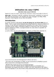
Using CQPIC Soft Processor - s.moutou@wanadoo.fr ou serge ...
Using CQPIC Soft Processor - s.moutou@wanadoo.fr ou serge ...
Using CQPIC Soft Processor - s.moutou@wanadoo.fr ou serge ...

You also want an ePaper? Increase the reach of your titles
YUMPU automatically turns print PDFs into web optimized ePapers that Google loves.
<strong>Using</strong> <strong>CQPIC</strong> <strong>Soft</strong> <strong>Processor</strong><br />
Last update : 2010-09-10<br />
Serge M<strong>ou</strong>t<strong>ou</strong><br />
System on Chip PIC16F84 on FPGA Xilinx<br />
Institut Universitaire de Technologie - Genie Électrique et Informatique Industrielle<br />
9, rue de Québec - BP 396 - 10026 TROYES cedex France<br />
(<strong>serge</strong>.m<strong>ou</strong>t<strong>ou</strong>@univ-reims.<strong>fr</strong>)<br />
Key words : softcore processor, SoC (System On Chip), C programming language and<br />
FPGA, FPGA Spartan3, Digilent Starter Board, VGA monitor, PIC®16F84<br />
Introduction<br />
The starting VHDL core and its last modifications are in :<br />
"http://m<strong>ou</strong>t<strong>ou</strong>.pagesperso-orange.<strong>fr</strong>/ER2/<strong>CQPIC</strong>Start.zip".<br />
The goal of this project is to construct a pong game interfaced to a VGA<br />
monitor with FPGA as a target chip. The pong game on VGA and on a FPGA is<br />
a classical subject and y<strong>ou</strong> can find a lot of examples on the Internet. But <strong>ou</strong>r<br />
goal is to use a <strong>fr</strong>ee 8-bit soft processor interacting with external hardware<br />
described in VHDL. The soft core which we refer to as <strong>CQPIC</strong> in this document,<br />
is compatible with the Microchip fam<strong>ou</strong>s PIC®16F84. We expect to program this<br />
soft core with C language.<br />
The target board is a digilent Board with a Xilinx FPGA, more exactly the<br />
1
Spartan-3 Starter Board see :<br />
System on Chip PIC16F84 on FPGA Xilinx<br />
http://www.digilentinc.com/Products/Catalog.cfm?NavPath=2,400&Cat=10<br />
Integrated Development Environment (IDE) used are then :<br />
- ISE Xilinx for VHDL programs or the <strong>fr</strong>ee WebPack<br />
(http://www.xilinx.com/support/download/).<br />
- MPLAB (http://www.microchip.com/stellent/idcplg?<br />
IdcService=SS_GET_PAGE&nodeId=1406&dDocName=en019469) for<br />
developing 8-bit PIC1657 applications in Windows NT/2000/XP/Vista/7<br />
environments and using assembler or Hi-Tech C (http://www.htsoft.com/). Hi-<br />
Tech C is <strong>fr</strong>ee for a lite version when installing MPLAB.<br />
This project is intended for two undergraduate students in third semester<br />
during 80 h<strong>ou</strong>rs.<br />
The <strong>CQPIC</strong> is a <strong>fr</strong>ee soft core (or soft processor) able to run the same<br />
instructions as microchip PIC® 16F84. Because this project is removed <strong>fr</strong>om<br />
OpenCores.org and then difficult to find, y<strong>ou</strong> can download my new version in<br />
the internet "http://perso.wanadoo.<strong>fr</strong>/m<strong>ou</strong>t<strong>ou</strong>/ER2/<strong>CQPIC</strong>Start.zip".<br />
It was developped by Sumio Morioka (Japan) and published in December 1999<br />
in "Transistor Gijutsu Magazine" (its last update was in 2004)<br />
Where do we start or choosing a Core<br />
At means three versions of compatible PIC® 16F84 soft processor can be f<strong>ou</strong>nd<br />
in the internet. The most recent is probably a Verilog project available at<br />
opencores : "http://opencores.org/project,risc16f84" with recent updates<br />
(2006). But with undergraduate students who have only skills on VHDL, I intend<br />
to use <strong>CQPIC</strong>, older, but at the origin of this verilog core.<br />
Last academic year, I have used and programmed a soft processor 16C57 and<br />
the corresponding report of the project is also available in the Internet<br />
"http://perso.wanadoo.<strong>fr</strong>/m<strong>ou</strong>t<strong>ou</strong>/ER2/SiliCore1657_en.pdf". This old project,<br />
which we refer to as silicore1657 in the following, allows me to acquire<br />
experience useful for choosing the core. An other VHDL core is also available<br />
which we refer to as PPX in the following (http://opencores.org/project,ppx16)<br />
<strong>fr</strong>om Daniel Wallner, used and debugged by Patrice N<strong>ou</strong>el, Maître de<br />
Conférence in ENSIERB (now retired). But my choice is the <strong>CQPIC</strong> core because<br />
it doesn't use bidirectional PORTs but three PORTs as explained further in this<br />
document.<br />
We first present the hardware core starting <strong>fr</strong>om Microchip documentation.<br />
PIC® 16F84 Architecture<br />
It is a 8-bit processor with a 14-bit wide instruction set. The original PIC 16F84<br />
has a only 68 bytes wide RAM. An other limitation is its stack : only eight levels.<br />
It's probably very hard to program a C compiler with this architecture but we<br />
have one for <strong>fr</strong>ee.<br />
2
System on Chip PIC16F84 on FPGA Xilinx<br />
This processor manage interrupts (only one interrupt vector but many s<strong>ou</strong>rces<br />
of interrupts).<br />
We begin with the more difficult part : the Register File. I use the word<br />
"difficult" only because of the memory banking, a microchip particularity even<br />
with more recent 8-bit microcontroller (till 18FXXX series) which only disapears<br />
with the new 16/32-bit architectures (24FXXX and others)<br />
The register File<br />
The register file is broken up into two banks as presented below.<br />
The register bank is selected by modifying the one bank selection bit RP0 of<br />
the STATUS register. The lower thirdteen registers in each bank are sometimes<br />
different sometimes identical. The sixtyheight SRAM registers in each bank all<br />
map back to BANK 0.<br />
General banked memory starts at 0x50 address and was not used in the 16F84.<br />
File<br />
Address<br />
Banque 0 Banque 1 File<br />
Address<br />
00h Indirect addr. Indirect addr. 80h<br />
bcf status,rp0 01h TMR0 OPTION_REG 81h bsf status,rp0<br />
passe en 02h PCL PCL 82h passe en<br />
banque 0 03h STATUS STATUS 83h banque 1<br />
04h FSR FSR 84h<br />
05h PORTA TRISA 85h<br />
06h PORTB TRISB 86h<br />
07h --- --- 87h<br />
08h EEDATA EECON1 88h<br />
09h EEADR EECON2 89h<br />
0Ah PCLATH PCLATH 8Ah<br />
0Bh INTCON INTCON 8Bh<br />
0Ch 68 cases<br />
mémoires<br />
... SRAM<br />
correspond à<br />
la banque 0<br />
8Ch<br />
4Fh CFh<br />
3
not used not used<br />
7Fh FFh<br />
System on Chip PIC16F84 on FPGA Xilinx<br />
Y<strong>ou</strong> can also see the addresses 07h and 87h are not used in 16F84 but we will<br />
use them in <strong>ou</strong>r core as explained further.<br />
Instructions Set<br />
The 35 instructions of PIC® 16F84 are now presented.<br />
Operands :<br />
- f : register file address <strong>fr</strong>om 00 to 7F<br />
- W : Working register (accumulator)<br />
- d : destination selection : d=0 store result in W , d=1 store result in f<br />
- bbb : Bit address within an 8-bit file register (3 bits)<br />
- k : Literal field, constant data or label (8, or 9 bits)<br />
- PC program c<strong>ou</strong>nter<br />
- TO Time Out bit<br />
- PD Power Down bit<br />
BYTE-ORIENTED FILE REGISTER OPERATIONS<br />
Mnemonic<br />
Operand<br />
Description Cycles 14 bits Opcode status<br />
affected<br />
ADDWF f,d Add W and f 1 00 0111 dfff ffff C,DC,Z 1,2<br />
ANDWF f,d AND W with f 1 00 0101 dfff ffff Z 1,2<br />
CLRF f Clear f 1 00 0001 1fff ffff Z 2<br />
CLRW - Clear W 1 00 0001 0xxx xxxx Z<br />
COMF f,d Complement f 1 00 1001 dfff ffff Z 1,2<br />
DECF f,d Decrement f 1 00 0011 dfff ffff Z 1,2<br />
notes<br />
DECFSZ f,d Decrement f (skip if 0) 1,(2) 00 1011 dfff ffff Z 1,2,3<br />
INCF f,d Increment f 1 00 1010 dfff ffff Z 1,2<br />
INCFSZ f,d Increment f (skip if 0) 1,(2) 00 1111 dfff ffff Z 1,2,3<br />
IORWF f,d Inclusive OR W with f 1 00 0100 dfff ffff Z 1,2<br />
MOVF f,d Move f 1 00 1000 dfff ffff Z 1,2<br />
MOVWF Move W to f 1 00 0000 1fff ffff<br />
4
System on Chip PIC16F84 on FPGA Xilinx<br />
NOP - No operation 1 00 0000 0xx0 0000<br />
RLF f,d Rotate left f thr<strong>ou</strong>gh Carry 1 00 1101 dfff ffff C 1,2<br />
RRF f,d Rotate right f thr<strong>ou</strong>gh Carry 1 00 1100 dfff ffff C 1,2<br />
SUBWF f,d subtract W <strong>fr</strong>om f 1 00 0010 dfff ffff C,DC,Z 1,2<br />
SWAPW f,d Swap f 1 00 1110 dfff ffff 1,2<br />
XORWF f,d Inclusive OR W with f 1 00 0110 dfff ffff Z 1,2<br />
BIT-ORIENTED FILE REGISTER OPERATIONS<br />
Mnémonic,<br />
Opérands<br />
Description Cycles 14 bits Opcode status<br />
affected<br />
BCF f,b Bit Clear f 1 01 00bb bfff ffff 1,2<br />
BSF f,b Bit Set f 1 01 01bb bfff ffff 1,2<br />
BTFSC f,b Bit Test f, Skip if Clear 1,(2) 01 10bb bfff ffff 1,2<br />
BTFSS f,b Bit Test f, Skip if Set 1,(2) 01 11bb bfff ffff 1,2<br />
LITERAL AND CONTROL OPERATIONS<br />
Mnémonic,<br />
Opérands<br />
Description Cycles 14 bits Opcode status<br />
affected<br />
ADDLW k Addition de W et k 1 11 111x kkkk kkkk C,DC,Z<br />
ANDLW k AND literal with W 1 11 1001 kkkk kkkk Z<br />
CALL k Call subr<strong>ou</strong>tine 2 10 0kkk kkkk kkkk<br />
CLRWDT - Clear Watchdog Timer 1 00 0000 0110 0100 /TO,/PD<br />
GOTO k Unconditional branch 2 10 1kkk kkkk kkkk<br />
IORLW inclusive OR literal with W 1 11 1000 kkkk kkkk Z<br />
MOVLW Move Literal to W 1 11 00xx kkkk kkkk<br />
RETFIE Return <strong>fr</strong>om interrupt 2 00 0000 0000 1001<br />
RETLW k Return, place Literal in W 2 11 01xx kkkk kkkk<br />
RETURN return <strong>fr</strong>om subprogram 2 00 0000 0000 1000<br />
5<br />
notes<br />
notes
System on Chip PIC16F84 on FPGA Xilinx<br />
SLEEP Go into standby mode 1 00 0000 0110 0011 /TO,/PD<br />
SUBLW k Go into standby mode 1 11 110x kkkk kkkk C,DC,Z<br />
XORLW exclusive OR literal with W 1 11 1010 kkkk kkkk Z<br />
Note 1: When an I/O register is modified as a function of itself ( e.g., MOVF PORTB, 1), the value<br />
used will be that value present on the pins themselves. For example, if the data latch is ’1’ for a<br />
pin configured as input and is driven low by an external device, the data will be written back<br />
with a ’0’.<br />
2: If this instruction is executed on the TMR0 register (and, where applicable, d = 1), the<br />
prescaler will be cleared if assigned to the Timer0 Module.<br />
3: If Program C<strong>ou</strong>nter (PC) is modified or a conditional test is true, the instruction requires<br />
two cycles. The second cycle is executed as a NOP.<br />
Create y<strong>ou</strong>r own microcontroller with the <strong>CQPIC</strong>.<br />
The <strong>CQPIC</strong> is delivered as a VHDL soft core module, and is intended for use in<br />
both ASIC and FPGA type devices.<br />
The Core<br />
The core is presented as a schematic and as a VHDL program.<br />
6
progdata(13:0)<br />
progadr(12:0)<br />
ramdtin(7:0)<br />
ramdt<strong>ou</strong>t(10:0)<br />
existeeprom<br />
ramadr(8:0)<br />
readram<br />
epdtin(7:0)<br />
writeram<br />
readeepack<br />
epdt<strong>ou</strong>t(7:0)<br />
writeepack<br />
eepadr(7:0)<br />
porta_in(7:0)<br />
readeepreq<br />
portb_in(7:0)<br />
rwriteepreq<br />
portc_in(7:0)<br />
porta_<strong>ou</strong>t(7:0)<br />
int0<br />
porta_dir(7:0)<br />
int4<br />
portb_<strong>ou</strong>t(7:0)<br />
int5<br />
portb_dir(7:0)<br />
int6<br />
portc_<strong>ou</strong>t(7:0)<br />
int7<br />
t0cki<br />
wdtena<br />
wdtclk<br />
ponrst_n<br />
mclr_n<br />
clkin<br />
portc_dir(7:0)<br />
portc_strobe<br />
wdtfull<br />
powerdown<br />
startclkin<br />
clk<strong>ou</strong>t<br />
System on Chip PIC16F84 on FPGA Xilinx<br />
entity piccore is<br />
generic (<br />
Y<strong>ou</strong> can change the following parameters as y<strong>ou</strong> w<strong>ou</strong>ld like<br />
STACK_SIZE : integer := 8;<br />
Size of PC stack<br />
WDT_SIZE : integer := 255<br />
Size of watch dog timer (WDT)<br />
);<br />
port (<br />
program ROM data bus/address bus<br />
progdata : in std_logic_vector(13 downto 0); ROM read data<br />
progadr : <strong>ou</strong>t std_logic_vector(12 downto 0); ROM address<br />
data RAM data bus/address bus/control signals<br />
ramdtin : in std_logic_vector(7 downto 0); RAM read data<br />
ramdt<strong>ou</strong>t : <strong>ou</strong>t std_logic_vector(7 downto 0); RAM write data<br />
ramadr : <strong>ou</strong>t std_logic_vector(8 downto 0);<br />
RAM address; ramadr(8..7) indicates RAMBANK<br />
readram : <strong>ou</strong>t std_logic; RAM read strobe (H active)<br />
writeram : <strong>ou</strong>t std_logic; RAM write strobe (H active)<br />
EEPROM data bus/address bus<br />
existeeprom : in std_logic; Set to '1' if EEPROM is implemented.<br />
eepdtin : in std_logic_vector(7 downto 0); EEPROM read data<br />
eepdt<strong>ou</strong>t : <strong>ou</strong>t std_logic_vector(7 downto 0); EEPROM write data<br />
eepadr : <strong>ou</strong>t std_logic_vector(7 downto 0); EEPROM address<br />
readeepreq : <strong>ou</strong>t std_logic; EEPROM read request (H active)<br />
readeepack : in std_logic; EEPROM read acknowledge (H active)<br />
writeeepreq : <strong>ou</strong>t std_logic; EEPROM write request (H active)<br />
writeeepack : in std_logic; EEPROM write acknowledge (H active)<br />
I/O ports<br />
porta_in : in std_logic_vector(7 downto 0); PORTA input data<br />
porta_<strong>ou</strong>t : <strong>ou</strong>tstd_logic_vector(7 downto 0); PORTA <strong>ou</strong>tput data<br />
TRISA: PORTA signal direction (H:input, L:<strong>ou</strong>tput)<br />
porta_dir : <strong>ou</strong>t std_logic_vector(7 downto 0);<br />
portb_in : in std_logic_vector(7 downto0); PORTB input data<br />
portb_<strong>ou</strong>t : <strong>ou</strong>t std_logic_vector(7 downto0); PORTB <strong>ou</strong>tput data<br />
TRISB: PORTB signal direction (H:input, L:<strong>ou</strong>tput)<br />
portb_dir : <strong>ou</strong>tstd_logic_vector(7 downto0);<br />
rbpu : <strong>ou</strong>tstd_logic; PORT_B pullup enable (usually not used)<br />
PORTB interrupt input<br />
int0 : in std_logic; PORTB(0) INT<br />
int4 : in std_logic; PORTB(4) INT<br />
int5 : in std_logic; PORTB(5) INT<br />
int6 : in std_logic; PORTB(6) INT<br />
int7 : in std_logic; PORTB(7) INT<br />
portc_in : in std_logic_vector(7downto0); PORTC input data<br />
portc_<strong>ou</strong>t : <strong>ou</strong>tstd_logic_vector(7downto0); PORTC <strong>ou</strong>tput data<br />
portc_dir : <strong>ou</strong>t std_logic_vector(7downto0); TRISC: PORTC signal direction<br />
portc_strob e: <strong>ou</strong>t std_logic; PORT_C strobe<br />
TMR0 Control<br />
t0cki : in std_logic; T0CKI (PORTA(4))<br />
Watch Dog Timer Control<br />
wdtena : in std_logic; WDT enable (H active)<br />
wdtclk : in std_logic; WDT clock<br />
wdtfull : <strong>ou</strong>tstd_logic; WDTfull indicator (H active)<br />
CPU clock stop/start indicators<br />
powerdown : <strong>ou</strong>t std_logic; SLEEPmode; if H, y<strong>ou</strong> can stop system clock clkin<br />
WAKEUP; if H, y<strong>ou</strong> sh<strong>ou</strong>ld turn on clock for waking up <strong>fr</strong>om sleepmode<br />
startclkin : <strong>ou</strong>t std_logic;<br />
CPU reset<br />
ponrst_n : in std_logic; Poweron reset (L active)<br />
mclr_n : in std_logic; Normal reset (L active)<br />
CPU clock<br />
clkin : in std_logic; Clock input<br />
clk<strong>ou</strong>t : <strong>ou</strong>t std_logic Clock <strong>ou</strong>tput (clkin/4)<br />
);<br />
end piccore;<br />
For this core, "progadr" is the ROM address bus, while "progdata" is the<br />
corresponding data bus of this ROM. The RAM is managed with "ramadr" as<br />
address bus and "ramdt<strong>ou</strong>t/ramdtin" as data bus.<br />
Please note that in the contrary of PIC® 16F84, the <strong>CQPIC</strong> use a dedicated<br />
7
System on Chip PIC16F84 on FPGA Xilinx<br />
entry TMRCLK for timer0 clock (for PIC® it's the b4 bit T0CKl of PORTA).<br />
Before going further with peripherals we will explore how the I/O ports are<br />
working in the next section.<br />
The two ports of <strong>CQPIC</strong><br />
I have modified the original core particularly PORTs managment. But they are<br />
presented further. Only generalities are presented in this section.<br />
Normally ports are bidirectional entities in a microcontroller. How to synthetize<br />
a bidirectional port is FPGA dependent and y<strong>ou</strong> cannot find a general working<br />
way. Then, no bidirectional ports can be f<strong>ou</strong>nd in the <strong>CQPIC</strong> core.<br />
In principle, a dedicated register manage bidirectionality. The corresponding<br />
registers are present in the core with the names PORTA and PORTB. They are<br />
all 8-bit wide in the contrary of original PIC® 16F84 where PORTA and TRISA<br />
are a 5-bit register. The I/O ports are in fact in ports named porta_in and<br />
portb_in, and <strong>ou</strong>t ports named porta_<strong>ou</strong>t and portb_<strong>ou</strong>t while directional<br />
commands are porta_dir and porta_dir.<br />
porta_dir(7:0)<br />
porta_in(7:0)<br />
porta_<strong>ou</strong>t(7:0)<br />
Input/Output bidirectional PORT<br />
In the opposite Figure, y<strong>ou</strong> see on the<br />
left three ports (of the <strong>CQPIC</strong>) and on<br />
the right one bidirectional port. Y<strong>ou</strong><br />
can use the three ports in this way or<br />
keep the ports with<strong>ou</strong>t any change :<br />
we will keep the three ports in <strong>ou</strong>r<br />
project.<br />
Remark : for compatibility reasons we write in the porti_dir port in a particular<br />
way. If i=A, writing in porta_dir is done with the C assertion :<br />
// C language<br />
PORTA(7:0)<br />
TRISA=0xFF; // 1 input<br />
and in assembly language we c<strong>ou</strong>ld write :<br />
; assembly language<br />
bsf STATUS,5 ; select memory bank 1<br />
movlw 255 ;1:input<br />
movwf TRISA ;<br />
As a second remark I w<strong>ou</strong>ld say that in original core the PORTA register was 5-<br />
8
System on Chip PIC16F84 on FPGA Xilinx<br />
bit wide. I have modified the core in <strong>CQPIC</strong>.VHD file to extend this port as a 8bit<br />
register (see in folder "\<strong>CQPIC</strong>Start\PORTA8"of <strong>CQPIC</strong>Start.zip file).<br />
The last remark is if we write a statement like :<br />
PORTA = PORTA; // une seule diode allumee<br />
in a C program it has the signification : porta_<strong>ou</strong>t
end if;<br />
end process;<br />
data<strong>ou</strong>t
use IEEE.std_logic_1164.all;<br />
use IEEE.numeric_std.all;<br />
entity progrom is<br />
port(<br />
Clk : in std_logic;<br />
romaddr : in std_logic_vector(12 downto 0);<br />
rom<strong>ou</strong>t : <strong>ou</strong>t std_logic_vector(13 downto 0)<br />
);<br />
end progrom;<br />
System on Chip PIC16F84 on FPGA Xilinx<br />
architecture rtl of progrom is<br />
signal A_r : std_logic_vector(12 downto 0);<br />
begin<br />
process (Clk)<br />
begin<br />
if Clk'event and Clk = '1' then<br />
A_r rom<strong>ou</strong>t rom<strong>ou</strong>t rom<strong>ou</strong>t rom<strong>ou</strong>t rom<strong>ou</strong>t rom<strong>ou</strong>t rom<strong>ou</strong>t rom<strong>ou</strong>t rom<strong>ou</strong>t rom<strong>ou</strong>t rom<strong>ou</strong>t rom<strong>ou</strong>t rom<strong>ou</strong>t rom<strong>ou</strong>t rom<strong>ou</strong>t
C with Assembly Language<br />
Let's begin with a C program with assembly.<br />
#include <br />
//#include serait-il mieux ?<br />
main(void)<br />
{<br />
#asm<br />
Start: bcf _STATUS,5 ; select memory bank 0<br />
movf _PORTA, W ;read PORTA<br />
bsf _STATUS,5 ; select memory bank 1<br />
movwf _TRISA ;Recopie de PORTA<br />
goto Start<br />
#endasm<br />
}<br />
System on Chip PIC16F84 on FPGA Xilinx<br />
This program is given as a demonstration. It doesn't do anything interesting<br />
and particularly not what stand in comments.<br />
Our first C program<br />
A simple C program is presented : recopy PORTA in PORTB.<br />
#include <br />
//#include w<strong>ou</strong>ld be better ?<br />
main(void)<br />
{ // La gestion de TRISA et TRISB semble importante dans ce coeur<br />
TRISA = 0xFF; // 8 inputs for A<br />
TRISB = 0x00; // 8 <strong>ou</strong>tputs for B<br />
while(1)<br />
PORTB = PORTA; // recopy of PORTA in PORTB which switch LEDs on<br />
}<br />
In the contrary of Silicore1657 already mentionned (last academic year), the<br />
<strong>CQPIC</strong> manage interrupts to which we turn with a simple example.<br />
Adding an interrupt<br />
Going further with <strong>ou</strong>r core means explore the interrupt mechanism. The<br />
simpler interrupt is probably the timer0 interrupt. We turn to the corresponding<br />
documentation.<br />
Timer0 Documentation<br />
Below is a block diagram which explain every thing y<strong>ou</strong> need to know for<br />
timer0.<br />
The OPTION register is the heart of the working options y<strong>ou</strong> select. For<br />
instance, only the three LSB bits are set to 1 for a division by 256. Because we<br />
want <strong>ou</strong>r eyes see the LEDs switch, this division is not great en<strong>ou</strong>gh : we will<br />
add a 16 division in the interrupt subprogram.<br />
12
Timer0<br />
b .................................. b<br />
7 0 OPTION<br />
Timer0<br />
Overflow (8 bits)<br />
b 7<br />
b 6<br />
b 5<br />
b 4<br />
b 3<br />
b 2<br />
b 1<br />
b 0<br />
TMR0IF<br />
INTCON<br />
b 7<br />
b 6<br />
b 5<br />
b 4<br />
b 3<br />
b 2<br />
b 1<br />
b 0<br />
T0CS<br />
T0SE<br />
PSA<br />
Timer0 in 16FXXX<br />
System on Chip PIC16F84 on FPGA Xilinx<br />
To make the timer0 working is easy but thr<strong>ou</strong>ghing an interrupt is something<br />
else. Again a block diagram will explain how interrupts work..<br />
INTCON<br />
0x0B Banque<br />
0 et 1<br />
GIE<br />
b 7<br />
b 6<br />
b 5<br />
b 4<br />
b 3<br />
b 2<br />
b 1<br />
b 0<br />
EEIE<br />
T0IE<br />
INTE<br />
RBIE<br />
T0IF<br />
INTF<br />
RBIF<br />
MUX 0<br />
1<br />
RBPU<br />
INTEDG<br />
T0PS2<br />
T0PS1<br />
T0PS0<br />
13<br />
MUX 0<br />
1<br />
2, 4, ...,256<br />
=2 (n+1)<br />
Interruption timer0<br />
Timer0<br />
&<br />
&<br />
&<br />
&<br />
Overflow<br />
b 8 ..................................... b 0<br />
4<br />
MCU<br />
Clock<br />
b 7<br />
b 6<br />
b 5<br />
b 4<br />
b 3<br />
b 2<br />
b 1<br />
b 0<br />
=1<br />
T0SE : S<strong>ou</strong>rce Edge select<br />
PORTA<br />
RA4/T0CKI
System on Chip PIC16F84 on FPGA Xilinx<br />
To realize the interrupt is done when a rising edge is present in the ellipse : we<br />
immediately deduce we have to set 1 in INTCON, exactly in T0IE and GIE.<br />
The Correponding Program<br />
Here is <strong>ou</strong>r first program with an interrupt.<br />
#include <br />
void interrupt decalage(void);<br />
unsigned char nb;<br />
main(void)<br />
{<br />
TRISA = 0xF9; // 6 entrees, 2 sorties p<strong>ou</strong>r A<br />
TRISB = 0x00; // 8 sorties p<strong>ou</strong>r B<br />
OPTION = 0x07; // prescaler 256 , entree sur quartz<br />
INTCON = 0xA0; // autorise l'interruption timer<br />
PORTB = 0x01; // une seule diode allumee<br />
TMR0 = 0x00 ;<br />
nb=0;<br />
while(1)<br />
{<br />
// on ne fait rien que recopier sur 2 segments la valeur de SW1<br />
if ((PORTA & 0x01) == 1) PORTA = 0x06;<br />
}<br />
}<br />
void interrupt decalage(void)<br />
{<br />
nb++;<br />
//TMR0 = 0x00; //c'est fait car overflow<br />
if (!(nb % 16))<br />
PORTB = (PORTB
1<br />
2<br />
3<br />
4<br />
5<br />
Horizontal and Vertical synchronization<br />
System on Chip PIC16F84 on FPGA Xilinx<br />
Horizontal and vertical synchronization timings are presented in the Figure<br />
below for a 640 by 480 resolution. To meet these times, we only use two<br />
c<strong>ou</strong>nters.<br />
Pixels RGB<br />
3,8 us<br />
64 us<br />
DB15<br />
Connector<br />
6<br />
11<br />
7<br />
12<br />
8<br />
13<br />
9<br />
14<br />
10<br />
15<br />
GND<br />
Figure 5-1: VGA Connections <strong>fr</strong>om Spartan-3 Starter Kit Board<br />
1,54 us<br />
1,02 ms<br />
Red<br />
Green<br />
Blue<br />
Horizontal Sync<br />
Vertical Sync<br />
Une ligne<br />
25,6 us<br />
480 lignes<br />
31,75 us<br />
15,24 ms<br />
16,6 ms<br />
15<br />
270?<br />
270?<br />
270?<br />
0,64 us<br />
0,35 ms<br />
(<strong>fr</strong>ont view)<br />
R<br />
G<br />
B<br />
HS<br />
VS<br />
(R12)<br />
(T12)<br />
(R11)<br />
(R9)<br />
(T10)<br />
(xx) = FPGA pin number<br />
UG130_c5_01_042604<br />
hsynch<br />
vsynch
System on Chip PIC16F84 on FPGA Xilinx<br />
Here is how things are working with two c<strong>ou</strong>nters (it's the "My_vga_synch.vhd"<br />
File content) :<br />
clock_25MHz<br />
T9<br />
0 -> 799<br />
h_c<strong>ou</strong>nt =699<br />
0 -> 524<br />
My_vga_synch.vhd<br />
h_c<strong>ou</strong>nt<br />
10<br />
10<br />
v_c<strong>ou</strong>nt<br />
658
clock_25MHz<br />
T9<br />
0 -> 799<br />
h_c<strong>ou</strong>nt =699<br />
0 -> 524<br />
10<br />
h_c<strong>ou</strong>nt<br />
10<br />
v_c<strong>ou</strong>nt<br />
System on Chip PIC16F84 on FPGA Xilinx<br />
Before coming back into programming subjects we present the top architecture<br />
with all the previ<strong>ou</strong>s components connected together.<br />
Assembly of Core, Memories and VGA Controller<br />
As shown in the above figure we need 2x10=20 bits to modify <strong>ou</strong>r<br />
ball/rectangle position. Because ports are 8 bits, we need f<strong>ou</strong>r ports only to<br />
manage the X and Y positions of the ball. But we have only two 8-bit <strong>ou</strong>tput<br />
PORTs (only because I extend the original PORTA).<br />
Why only two Output PORTs<br />
658
TRISA = PORTA ;<br />
System on Chip PIC16F84 on FPGA Xilinx<br />
A connection between PORTA (ra_<strong>ou</strong>t) and switchs is done in VHDL (with ucf<br />
file in fact) and TRISA (ra_dir) is connected to LEDs. If PORTA is set to OxFF<br />
(with external switch) before the core starts, every set of a switch to 0 will<br />
correctly switch off the corresponding LED. But y<strong>ou</strong> will be unable to switch<br />
back the LED on.<br />
Conclusion : Both PORTs TRIS (externally porta_dir and portb_dir) of the<br />
<strong>CQPIC</strong> core sh<strong>ou</strong>ld never be used as a general purpose <strong>ou</strong>tput<br />
PORT.<br />
How can we get r<strong>ou</strong>nd this difficulty ?<br />
Adding a PORTC in the <strong>CQPIC</strong><br />
(The correponding core is available in the folder"\<strong>CQPIC</strong>Start\PORTC" of<br />
<strong>CQPIC</strong>Start.zip file in http://perso.wanadoo.<strong>fr</strong>/m<strong>ou</strong>t<strong>ou</strong>/ER2/<strong>CQPIC</strong>Start.zip).<br />
After spending many h<strong>ou</strong>rs to extend the 5-bit PORTA to 8-bit, I have seen<br />
every code places where I can easily add a PORTC to the <strong>CQPIC</strong>. Is this<br />
extension a solution for finding 20-bit in ports ? Not at all because as already<br />
explained, adding a PORTC will only gives us three <strong>ou</strong>tput ports. I finally make<br />
this change in the core... and add also a corresponding strobe signal. With this<br />
strobe signal, I am able to add easily as many ports as I want.<br />
Please also note this solution lead us to declare the new PORTC and TRISC in<br />
<strong>ou</strong>r C programs. Because it's a bad idea to modify pic1684.h file, the snippet<br />
below shows the way directly in the C program :<br />
#include // <strong>ou</strong> #include <br />
volatile unsigned char PORTC @ 0x07;<br />
volatile unsigned char TRISC @ 0x87;<br />
It's very simple but not useful for particular bits access (we don't use bit access<br />
in <strong>ou</strong>r project).<br />
Let's turn now to the complete solution.<br />
Adding a "strobe" to PORTC and managing more ports<br />
A "strobe" signal is an <strong>ou</strong>tput which indicates when we write in the PORTC.<br />
With this signal it is easy to extend the number of ports untill 256. We give an<br />
example below showing how to extend to eight the nomber of PORTs. PORTA<br />
is used to select where is the final destination and PORTC is used to give the<br />
value. A block diagram will help for explanations.<br />
18
7<br />
b 6<br />
b 5<br />
b 4<br />
b 3<br />
b 2<br />
b 1<br />
b 0<br />
PORTC<br />
portc_strobe<br />
b 7<br />
b 6<br />
b 5<br />
b 4<br />
b 3<br />
b 2<br />
b 1<br />
b 0<br />
PORTA<br />
OUT_PORTA[7:0]<br />
Decoding<br />
Logic<br />
PORT_ID[2:0]<br />
System on Chip PIC16F84 on FPGA Xilinx<br />
How things work is easy to follow with this block diagram. The PORTC (on the<br />
left) is connected to every added ports (on the right) and the decoding logic<br />
will send the strobe signal to the port selected with PORTA for a recopy of the<br />
value of PORTC.<br />
Conclusion : The lack of one (or more) "strobe" signal in the original core is<br />
annoying when interfacing external hardware. Even if this<br />
doesn't lead to an interfacing impossibility, I think it's a good<br />
thing to add a PORTC and the corresponding strobe.<br />
The corresponding VHDL program of the above block diagram is given below. It<br />
uses two inputs PORTA and PORTC to realize f<strong>ou</strong>r <strong>ou</strong>tput ports pA, pB, pC, pD in<br />
a little different way : f<strong>ou</strong>r LSB bits of PORTA are used for the selection.<br />
-- increase the number of available ports with the new portC and<br />
its strobe<br />
-- ver1.10b, 2010/05/22 (Serge M<strong>ou</strong>t<strong>ou</strong>)<br />
library ieee;<br />
use ieee.std_logic_1164.all;<br />
19<br />
d q<br />
rd<br />
d<br />
rd<br />
d<br />
rd<br />
d<br />
rd<br />
8 bits<br />
q<br />
8 bits<br />
q<br />
8 bits<br />
q<br />
8 bits
System on Chip PIC16F84 on FPGA Xilinx<br />
entity ports is<br />
port(<br />
clk : in std_logic;<br />
strobeC_in : in std_logic;<br />
portA : in std_logic_vector(7 downto 0);<br />
portC : in std_logic_vector(7 downto 0);<br />
pA,pB,pC,pD : <strong>ou</strong>t std_logic_vector(7 downto 0) --new ports<br />
);<br />
end ports;<br />
architecture BehPorts of ports is<br />
signal Internal_strobes : std_logic_vector(7 downto 0);<br />
begin<br />
dmux_Strobe:process(portA,strobeC_in) begin<br />
case portA is<br />
when "00000001" => Internal_strobes(0) Internal_strobes(1) Internal_strobes(2) Internal_strobes(3) internal_strobes '0');<br />
end case;<br />
end process;<br />
port_A:process(clk)begin<br />
if clk'event and clk='1' then<br />
if Internal_strobes="00000001" then<br />
pA
System on Chip PIC16F84 on FPGA Xilinx<br />
means it's now possible to move a rectangle a ball with a program.<br />
C Programming<br />
Let's begin with a subprogram which write a 16-bit value in two new PORTs.<br />
The "setX" function<br />
With C language it c<strong>ou</strong>ld be done like as follow :<br />
void set(unsigned int x){<br />
TRISA=0x00;TRISC=0x00;<br />
PORTA=1;<br />
PORTC=x; //poids faible<br />
PORTA=2;<br />
PORTC=x>>8;//poids fort<br />
}<br />
The hardware completly determines the content of this subr<strong>ou</strong>tine.<br />
A horizontal B<strong>ou</strong>ncing Ball<br />
Here is <strong>ou</strong>r first program which shows a continu<strong>ou</strong>sly horizontal b<strong>ou</strong>ncing ball.<br />
#include <br />
volatile unsigned char PORTC @ 0x07;<br />
volatile unsigned char TRISC @ 0x87;<br />
void setX(unsigned int x);<br />
void setY(unsigned int y);<br />
void wait(int tempo);<br />
void main(){<br />
int i;<br />
while(1){<br />
setY(321);<br />
for(i=0;i>8;<br />
}<br />
void setY(unsigned int y){<br />
TRISA=0x00;TRISC=0x00;<br />
PORTA=4; //poids faible<br />
21
PORTC=x;<br />
PORTA=8;//poids fort<br />
PORTC=x>>8;<br />
}<br />
void wait(unsigned char tempo){<br />
OPTION=0x07; // div 256 et s<strong>ou</strong>rce=quartz<br />
TMR0 =0;<br />
while(TMR0=620) && (deltaX>0)) deltaX= -deltaX;<br />
if ((posX0)) deltaY= -deltaY;<br />
if ((posY8;<br />
}<br />
void setY(unsigned int y){<br />
TRISA=0x00;TRISC=0x00;<br />
PORTA=4; //poids faible<br />
PORTC=x;<br />
PORTA=8;//poids fort<br />
PORTC=x>>8;<br />
}<br />
22<br />
System on Chip PIC16F84 on FPGA Xilinx
void wait(unsigned char tempo){<br />
OPTION=0x07; // div 256 et s<strong>ou</strong>rce=quartz<br />
TMR0 =0;<br />
while(TMR0srow, col=>scol,r ed1=>sred, green1=>sgreen, blue1=>sblue,<br />
colorRGB=>"111", delta_x=>"0000001010", delta_y=>"0000001100",<br />
x_rec => x_rect, y_rec => y_rect);<br />
raquetteG:rect port map(row=>srow, col=>scol, red1=>sred1, green1=>sgreen1,<br />
blue1=>sblue1, colorRGB=>"100", delta_x=>"0000001010",<br />
delta_y=>"0000111010", x_rec => "0000010110",<br />
y_rec(8 downto 1) => y_raquG, y_rec(9)=>'0',y_rec(0)=>'0');<br />
23
aquetteD:rect port map(row=>srow, col=>scol, red1=>sred2, green1=>sgreen2,<br />
blue1=>sblue2,colorRGB=>"100", delta_x=>"0000001010",<br />
delta_y=>"0000111010", x_rec => "1001001000",<br />
y_rec(8 downto 1) => y_raquD,y_rec(9)=>'0',y_rec(0)=>'0');<br />
red
System on Chip PIC16F84 on FPGA Xilinx<br />
As can be easily seen, we choose sw0,sw1,sw6 and sw7 switchs of the board<br />
connected to input PORTB to move up and down the rackets and sw2 (RC2) for<br />
the start.<br />
What y<strong>ou</strong>r Work consists of ?<br />
The complete understanding of hardware (project<br />
preparation)<br />
Y<strong>ou</strong> have to be able to draw all the components and their connections starting<br />
<strong>fr</strong>om the given VHDL files ("\<strong>CQPIC</strong>Start\VGA_Pong" folder of <strong>CQPIC</strong>Start.zip<br />
file).<br />
Extend the Hardware (project preparation)<br />
Y<strong>ou</strong> have to extend the harware and then manage the rackets positions. Y<strong>ou</strong><br />
can choose to manage both the Y coordinates of each racket with one 8-bit port<br />
(leading then the hardware with 6 ports) or with 10-bit (leading then the<br />
hardware with 8 ports)<br />
Developping in C language<br />
Design a C program for managing rackets move with first the switchs and<br />
second the joysticks.<br />
Bresenham Line Algorithm<br />
Explore if it is possible to use Bresenham's line algorithm for trajectories and so<br />
enlarge considerably the number of them. This algorithm is explain in WIKI :<br />
http://en.wikipedia.org/wiki/Bresenham's_line_algorithm<br />
Y<strong>ou</strong> can directly find a C version in the Internet : google Bresenham in C.<br />
Managing Scores<br />
Use the bottom of the VGA monitor to print scores in character mode.Every<br />
time a ball is lost a new score is printed.<br />
Acknowledgements<br />
Thanks to Xilinx University Program for giving us gracefully five Digilent S3<br />
Starter Board used in <strong>ou</strong>r students projects and practices.<br />
Written with OpenOffice 2.4.1 under Linux<br />
25
System on Chip PIC16F84 on FPGA Xilinx<br />
APPENDIX I (transforming a HEX into VHDL)<br />
The complete C++ program to transform the hex file into a VHDL file is not<br />
given here because its size. Y<strong>ou</strong> can find it in "\<strong>CQPIC</strong>Start\ROM" folder of<br />
"http://perso.wanadoo.<strong>fr</strong>/m<strong>ou</strong>t<strong>ou</strong>/ER2/<strong>CQPIC</strong>Start.zip" file.<br />
Attention : I have not used the original hex2vhd.c file we can find in <strong>CQPIC</strong><br />
core because it never works correctly. I have taken the C++ hex2rom.cpp file<br />
y<strong>ou</strong> can find in the concurent PPX project. This file is slightly modified to fit<br />
directly in <strong>ou</strong>r VHDL project.<br />
When compiled the binary executable is named hex2rom.exe (under Windows)<br />
or hex2rom under Linux.<br />
Use the command line :<br />
hex2rom demo16F84.hex progrom 13l14s >progrom.vhd<br />
if the starting file is demo16F84.hex.<br />
The destination file is progrom.vhd with "progrom" as entity.<br />
13 means 13-bit address,<br />
l means little indian convention (b w<strong>ou</strong>ld be big indian)<br />
14 means 14-bit data ROM.<br />
26
System on Chip PIC16F84 on FPGA Xilinx<br />
Appendix II VHDL module to manage VGA<br />
Here is a complete VHDL module to manage completly VGA synchronization<br />
with a ball and two rackets (see "\<strong>CQPIC</strong>Start\VGA_Pong" folder of<br />
<strong>CQPIC</strong>Start.zip file).<br />
-- ************* My_vga_synch.vhd ***********<br />
library IEEE;<br />
use IEEE.STD_LOGIC_1164.all;<br />
use IEEE.STD_LOGIC_ARITH.all;<br />
use IEEE.STD_LOGIC_UNSIGNED.all;<br />
ENTITY VGA_SYNC IS<br />
PORT( clock_25Mhz : IN STD_LOGIC;<br />
horiz_sync_<strong>ou</strong>t, vert_sync_<strong>ou</strong>t : OUT STD_LOGIC;<br />
pixel_row, pixel_column: OUT STD_LOGIC_VECTOR(9 DOWNTO 0));<br />
END VGA_SYNC;<br />
ARCHITECTURE a OF VGA_SYNC IS<br />
SIGNAL horiz_sync, vert_sync : STD_LOGIC;<br />
SIGNAL h_c<strong>ou</strong>nt, v_c<strong>ou</strong>nt :STD_LOGIC_VECTOR(9 DOWNTO 0);<br />
BEGIN<br />
--Generate Horizontal and Vertical Timing Signals for Video Signal<br />
-- H_c<strong>ou</strong>nt c<strong>ou</strong>nts pixels (640 + extra time for sync signals)<br />
--<br />
-- Horiz_sync ------------------------------------__________--------<br />
-- H_c<strong>ou</strong>nt 0 640 659 755 799<br />
--<br />
gestion_H_C<strong>ou</strong>nt:PROCESS(clock_25Mhz) BEGIN<br />
IF(clock_25Mhz'EVENT) AND (clock_25Mhz='1') THEN<br />
IF (h_c<strong>ou</strong>nt = 799) THEN<br />
h_c<strong>ou</strong>nt '0');<br />
ELSE<br />
h_c<strong>ou</strong>nt = 524) AND (h_c<strong>ou</strong>nt >= 699) THEN<br />
v_c<strong>ou</strong>nt '0');<br />
ELSIF (h_c<strong>ou</strong>nt = 699) THEN<br />
27
v_c<strong>ou</strong>nt hsynch,<br />
vert_sync_<strong>ou</strong>t=>vsynch, pixel_row=>srow, pixel_column=>scol);<br />
balle:rect port map(row=>srow, col=>scol, red1=>sred, green1=>sgreen,<br />
blue1=>sblue,colorRGB=>"111",<br />
delta_x=>"0000001010",delta_y=>"0000001100",<br />
x_rec => x_rect, y_rec => y_rect);<br />
raquetteG:rect port map(row=>srow, col=>scol, red1=>sred1, green1=>sgreen1,<br />
blue1=>sblue1,colorRGB=>"100",<br />
delta_x=>"0000001010",delta_y=>"0000111010",<br />
28
System on Chip PIC16F84 on FPGA Xilinx<br />
x_rec => "0000010110", y_rec(8 downto 1) => y_raquG,<br />
y_rec(9)=>'0',y_rec(0)=>'0');<br />
raquetteD:rect port map(row=>srow, col=>scol, red1=>sred2, green1=>sgreen2,<br />
blue1=>sblue2, colorRGB=>"100",<br />
delta_x=>"0000001010",delta_y=>"0000111010",<br />
x_rec => "1001001000", y_rec(8 downto 1) => y_raquD,<br />
y_rec(9)=>'0',y_rec(0)=>'0');<br />
red
Appendix III (ucf File)<br />
#PORTB sur leds<br />
net "rb0_<strong>ou</strong>t" loc="K12";<br />
net "rb1_<strong>ou</strong>t" loc="P14";<br />
net "rb2_<strong>ou</strong>t" loc="L12";<br />
net "rb3_<strong>ou</strong>t" loc="N14";<br />
net "rb4_<strong>ou</strong>t" loc="P13";<br />
net "rb5_<strong>ou</strong>t" loc="N12";<br />
net "rb6_<strong>ou</strong>t" loc="P12";<br />
net "rb7_<strong>ou</strong>t" loc="P11";<br />
#PORTB sur interrupteurs<br />
net "rb_in" loc="k13";<br />
net "rb_in" loc="k14";<br />
net "rb_in" loc="j13";<br />
net "rb_in" loc="j14";<br />
net "rb_in" loc="h13";<br />
net "rb_in" loc="h14";<br />
net "rb_in" loc="g12";<br />
net "rb_in" loc="f12";<br />
#sept segments<br />
#net "sorties" loc="E14";<br />
#net "sorties" loc="G13";<br />
#net "sorties" loc="N15";<br />
#net "sorties" loc="P15";<br />
#net "sorties" loc="R16";<br />
#net "sorties" loc="F13";<br />
#net "sorties" loc="N16";<br />
#selection afficheurs<br />
#net "affpdsfaible" loc="D14";<br />
#net "affpdsfort" loc="G14";<br />
# clock<br />
net "clkin" loc="T9";<br />
net "clkin" TNM_NET = "clkin";<br />
TIMESPEC "TS_mclk" = PERIOD "clkin" 20 ns HIGH 50 %;<br />
# reset<br />
net "mclr_n" loc="M13";<br />
net "ponrst_n" loc="M14";<br />
#VGA<br />
net "hsynch" loc="R9";<br />
net "vsynch" loc="T10";<br />
net "red" loc="R12";<br />
net "blue" loc="R11";<br />
net "green" loc="T12";<br />
30<br />
System on Chip PIC16F84 on FPGA Xilinx
Appendix IV (pong.vhd File)<br />
System on Chip PIC16F84 on FPGA Xilinx<br />
Here is the VHDL file at the top of the hierarchy describing then how<br />
components are connected (see "\<strong>CQPIC</strong>Start\VGA_Pong" folder of<br />
<strong>CQPIC</strong>Start.zip file) :<br />
library IEEE;<br />
use IEEE.STD_LOGIC_1164.all;<br />
entity pong is<br />
PORT (<br />
rb_in : in std_logic_vector(7 downto 0);<br />
ponrst_n : in std_logic;<br />
mclr_n : in std_logic;<br />
clkin : in std_logic;<br />
hsynch,vsynch,red,green,blue : <strong>ou</strong>t STD_LOGIC<br />
);<br />
end pong;<br />
architecture beh_pong of pong is<br />
component cqpic<br />
port (<br />
ra_in : in std_logic_vector(7 downto 0);<br />
rb_in : in std_logic_vector(7 downto 0);<br />
ponrst_n : in std_logic;<br />
mclr_n : in std_logic;<br />
clkin : in std_logic;<br />
wdtena : in std_logic;<br />
wdtclk : in std_logic;<br />
ra_<strong>ou</strong>t : <strong>ou</strong>t std_logic_vector(7 downto 0);<br />
rb_<strong>ou</strong>t : <strong>ou</strong>t std_logic_vector(7 downto 0);<br />
ra_dir : <strong>ou</strong>t std_logic_vector(7 downto 0);<br />
rb_dir : <strong>ou</strong>t std_logic_vector(7 downto 0);<br />
rc_<strong>ou</strong>t, rc_dir : <strong>ou</strong>t std_logic_vector(7 downto 0); --<br />
PORT-C data<br />
rc_in : in std_logic_vector(7 downto 0);<br />
rd_<strong>ou</strong>t : <strong>ou</strong>t std_logic_vector(7 downto 0); -- (added PORT-D<br />
data)<br />
re_<strong>ou</strong>t : <strong>ou</strong>t std_logic_vector(7 downto 0); -- (added PORT-E<br />
data)<br />
clk<strong>ou</strong>t : <strong>ou</strong>t std_logic;<br />
wdtfull : <strong>ou</strong>t std_logic;<br />
powerdown : <strong>ou</strong>t std_logic;<br />
startclkin : <strong>ou</strong>t std_logic<br />
);<br />
end component;<br />
component VGAtop<br />
PORT (clk_50 : in STD_LOGIC;<br />
x_rect, y_rect: IN STD_LOGIC_VECTOR(9 DOWNTO 0);<br />
y_raquG, y_raquD: IN STD_LOGIC_VECTOR(7 DOWNTO 0);<br />
hsynch,vsynch,red,green,blue : <strong>ou</strong>t STD_LOGIC);<br />
END component;<br />
signal s_x_rect, s_y_rect : STD_LOGIC_VECTOR(9 DOWNTO 0);<br />
signal s_rb, s_re : STD_LOGIC_VECTOR(5 DOWNTO 0);<br />
begin<br />
core : cqpic port map(<br />
ra_in => "00000000",<br />
rb_in => rb_in,<br />
rc_in => "00000000",<br />
ponrst_n => ponrst_n,<br />
mclr_n => mclr_n,<br />
clkin => clkin,<br />
31
wdtena => '0',<br />
wdtclk => '0',<br />
ra_<strong>ou</strong>t => s_x_rect(7 downto 0),<br />
rb_<strong>ou</strong>t(1 downto 0) => s_x_rect(9 downto 8),<br />
rb_<strong>ou</strong>t(7 downto 2) => s_rb,<br />
rd_<strong>ou</strong>t => s_y_rect(7 downto 0),<br />
re_<strong>ou</strong>t(1 downto 0) => s_y_rect(9 downto 8),<br />
re_<strong>ou</strong>t(7 downto 2) => s_re<br />
);<br />
vga:VGATop port map (<br />
clk_50 => clkin,<br />
x_rect => s_x_rect,<br />
y_rect => s_y_rect,<br />
y_raquG => "00000000",<br />
y_raquD => "00000000",<br />
hsynch => hsynch,<br />
vsynch => vsynch,<br />
red => red,<br />
green => green,<br />
blue => blue<br />
);<br />
end beh_pong;<br />
32<br />
System on Chip PIC16F84 on FPGA Xilinx