Current Mode PWM Controller (Rev. A)
Current Mode PWM Controller (Rev. A) Current Mode PWM Controller (Rev. A)
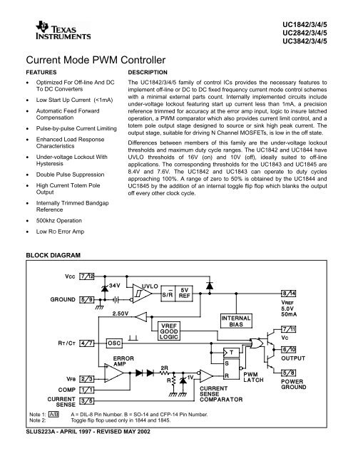
Current Mode PWM Controller FEATURES • Optimized For Off-line And DC To DC Converters • Low Start Up Current (
- Page 2 and 3: ABSOLUTE MAXIMUM RATINGS(Note 1) Su
- Page 4 and 5: UC1842/3/4/5 UC2842/3/4/5 UC3842/3/
- Page 6 and 7: UC1842/3/4/5 UC2842/3/4/5 OUTPUT SA
- Page 8 and 9: PACKAGE OPTION ADDENDUM www.ti.com
- Page 10 and 11: PACKAGE OPTION ADDENDUM www.ti.com
- Page 13 and 14: MECHANICAL DATA MLCC006B - OCTOBER
- Page 16: MECHANICAL DATA MPLC004A - OCTOBER
<strong>Current</strong> <strong>Mode</strong> <strong>PWM</strong> <strong>Controller</strong><br />
FEATURES<br />
• Optimized For Off-line And DC<br />
To DC Converters<br />
• Low Start Up <strong>Current</strong> (
ABSOLUTE MAXIMUM RATINGS(Note 1)<br />
Supply Voltage (Low Impedance Source) ..............30V<br />
Supply Voltage (ICC < 30mA) .................Self Limiting<br />
Output <strong>Current</strong>. ..................................±1A<br />
Output Energy (Capacitive Load) ....................5µJ<br />
Analog Inputs (Pins 2, 3). ..................-0.3V to +6.3V<br />
Error Amp Output Sink <strong>Current</strong> ....................10mA<br />
Power Dissipation at TA ≤ 25°C (DIL−8).................1W<br />
Power Dissipation at TA ≤ 25°C (SOIC-14) .........725mW<br />
Storage Temperature Range. .............-65°C to +150°C<br />
Junction Temperature Range .............-55°C to +150°C<br />
Lead Temperature (soldering, 10 seconds) ...........300°C<br />
Note 1: All voltages are with respect to Pin 5.<br />
All currents are positive into the specified terminal.<br />
Consult Packaging Section of Databook for thermal<br />
limitations and considerations of packages.<br />
UC1842/3/4/5<br />
UC2842/3/4/5<br />
UC3842/3/4/5<br />
CONNECTION DIAGRAMS<br />
DIL-8, SOIC-8 (TOP VIEW)<br />
N or J Package, D8 Package<br />
PLCC-20 (TOP VIEW)<br />
Q Package<br />
SOIC-14, CFP-14. (TOP VIEW)<br />
D or W Package<br />
PACKAGE PIN FUNCTION<br />
FUNCTION<br />
PIN<br />
N/C 1<br />
COMP 2<br />
N/C 3<br />
N/C 4<br />
VFB 5<br />
N/C 6<br />
ISENSE 7<br />
N/C 8<br />
N/C 9<br />
RT/CT 10<br />
N/C 11<br />
PWR GND 12<br />
GROUND 13<br />
N/C 14<br />
OUTPUT 15<br />
N/C 16<br />
VC 17<br />
VCC 18<br />
N/C 19<br />
VREF 20<br />
DISSIPATION RATING TABLE<br />
Package TA ≤ 25°C Derating Factor TA ≤ 70°C<br />
TA ≤ 85°C TA ≤ 125°C<br />
Power Rating Above TA ≤ 25°C Power Rating Power Rating Power Rating<br />
W 700 mW 5.5 mW/°C 452 mW 370 mW 150 mW<br />
2
ELECTRICAL CHARACTERISTICS:<br />
UC1842/3/4/5<br />
UC2842/3/4/5<br />
UC3842/3/4/5<br />
Unless otherwise stated, these specifications apply for -55°C ≤ TA ≤ 125°C for the<br />
UC184X; -40°C ≤ TA ≤ 85°C for the UC284X; 0°C ≤ TA ≤ 70°C for the 384X; VCC = 15V<br />
(Note 5); RT = 10k; CT = 3.3nF, TA=TJ.<br />
UC1842/3/4/5 UC3842/3/4/5 UNITS<br />
PARAMETER<br />
TEST CONDITIONS<br />
UC2842/3/4/5<br />
MIN TYP MAX MIN TYP MAX<br />
Reference Section<br />
Output Voltage TJ = 25°C, IO = 1mA 4.95 5.00 5.05 4.90 5.00 5.10 V<br />
Line Regulation 12 ≤ VIN ≤ 25V 6 20 6 20 mV<br />
Load Regulation 1 ≤ I0 ≤ 20mA 6 25 6 25 mV<br />
Temp. Stability (Note 2) (Note 7) 0.2 0.4 0.2 0.4 mV/°C<br />
Total Output Variation Line, Load, Temp. (Note 2) 4.9 5.1 4.82 5.18 V<br />
Output Noise Voltage 10Hz ≤ f ≤ 10kHz, TJ = 25°C (Note2) 50 50 µV<br />
Long Term Stability TA = 125°C, 1000Hrs. (Note 2) 5 25 5 25 mV<br />
Output Short Circuit -30 -100 -180 -30 -100 -180 mA<br />
Oscillator Section<br />
Initial Accuracy TJ = 25°C (Note 6) 47 52 57 47 52 57 kHz<br />
Voltage Stability 12 ≤ VCC ≤ 25V 0.2 1 0.2 1 %<br />
Temp. Stability TMIN ≤ TA ≤ TMAX (Note 2) 5 5 %<br />
Amplitude VPIN 4 peak to peak (Note 2) 1.7 1.7 V<br />
Error Amp Section<br />
Input Voltage VPIN 1 = 2.5V 2.45 2.50 2.55 2.42 2.50 2.58 V<br />
Input Bias <strong>Current</strong> -0.3 -1 -0.3 -2 µA<br />
AVOL 2 ≤ VO ≤ 4V 65 90 65 90 dB<br />
Unity Gain Bandwidth (Note 2) TJ = 25°C 0.7 1 0.7 1 MHz<br />
PSRR 12 ≤ VCC ≤ 25V 60 70 60 70 dB<br />
Output Sink <strong>Current</strong> VPIN 2 = 2.7V, VPIN 1 = 1.1V 2 6 2 6 mA<br />
Output Source <strong>Current</strong> VPIN 2 = 2.3V, VPIN 1 = 5V -0.5 -0.8 -0.5 -0.8 mA<br />
VOUT High VPIN 2 = 2.3V, RL = 15k to ground 5 6 5 6 V<br />
VOUT Low VPIN 2 = 2.7V, RL = 15k to Pin 8 0.7 1.1 0.7 1.1 V<br />
<strong>Current</strong> Sense Section<br />
Gain (Notes 3 and 4) 2.85 3 3.15 2.85 3 3.15 V/V<br />
Maximum Input Signal VPIN 1 = 5V (Note 3) 0.9 1 1.1 0.9 1 1.1 V<br />
PSRR 12 ≤ V CC ≤ 25V (Note 3) (Note 2) 70 70 dB<br />
Input Bias <strong>Current</strong> -2 -10 -2 -10 µA<br />
Delay to Output VPIN 3 = 0 to 2V (Note 2) 150 300 150 300 ns<br />
Note 2: These parameters, although guaranteed, are not 100% tested in production.<br />
Note 3: Parameter measured at trip point of latch with VPIN 2 =0.<br />
Note 4: Gain defined as<br />
∆ VPIN 1<br />
A = ≤VPIN<br />
≤ V<br />
∆ VPIN 3 , 0 3 08 .<br />
Note 5: Adjust VCC above the start threshold before setting at 15V.<br />
Note 6: Output frequency equals oscillator frequency for the UC1842 and UC1843.<br />
Output frequency is one half oscillator frequency for the UC1844 and UC1845.<br />
Note 7: Temperature stability, sometimes referred to as average temperature coefficient, is described by the equation:<br />
VREF<br />
( max) − VREF ( min)<br />
Temp Stability =<br />
TJ ( max) − TJ ( min)<br />
VREF (max) and VREF (min) are the maximum and minimum reference voltages measured over the appropriate<br />
temperature range. Note that the extremes in voltage do not necessarily occur at the extremes in temperature.<br />
3
UC1842/3/4/5<br />
UC2842/3/4/5<br />
UC3842/3/4/5<br />
ELECTRICAL CHARACTERISTICS: Unless otherwise stated, these specifications apply for −55°C ≤ TA ≤ 125°C for the<br />
UC184X; −40°C ≤ TA ≤ 85°C for the UC284X; 0°C ≤ TA ≤ 70°C for the 384X; VCC =<br />
15V (Note 5); RT = 10k; CT = 3.3nF, TA=TJ.<br />
UC1842/3/4/5 UC3842/3/4/5 UNITS<br />
PARAMETER<br />
TEST CONDITION<br />
UC2842/3/4/5<br />
MIN TYP MAX MIN TYP MAX<br />
Output Section<br />
Output Low Level ISINK = 20mA 0.1 0.4 0.1 0.4 V<br />
ISINK = 200mA 1.5 2.2 1.5 2.2 V<br />
Output High Level ISOURCE = 20mA 13 13.5 13 13.5 V<br />
ISOURCE = 200mA 12 13.5 12 13.5 V<br />
Rise Time TJ = 25°C, CL = 1nF (Note 2) 50 150 50 150 ns<br />
Fall Time TJ = 25°C, CL = 1nF (Note 2) 50 150 50 150 ns<br />
Under-voltage Lockout Section<br />
Start Threshold X842/4 15 16 17 14.5 16 17.5 V<br />
X843/5 7.8 8.4 9.0 7.8 8.4 9.0 V<br />
Min. Operating Voltage X842/4 9 10 11 8.5 10 11.5 V<br />
After Turn On<br />
X843/5 7.0 7.6 8.2 7.0 7.6 8.2 V<br />
<strong>PWM</strong> Section<br />
Maximum Duty Cycle X842/3 95 97 100 95 97 100 %<br />
X844/5 46 48 50 47 48 50 %<br />
Minimum Duty Cycle 0 0 %<br />
Total Standby <strong>Current</strong><br />
Start-Up <strong>Current</strong> 0.5 1 0.5 1 mA<br />
Operating Supply <strong>Current</strong> VPIN 2 =VPIN 3 = 0V 11 17 11 17 mA<br />
VCC Zener Voltage ICC = 25mA 30 34 30 34 V<br />
Note 2: These parameters, although guaranteed, are not 100% tested in production.<br />
Note 3: Parameter measured at trip point of latch with VPIN 2 =0<br />
.<br />
Note 4:<br />
∆ VPIN 1<br />
Gain defined as: A = ≤VPIN<br />
≤ V<br />
∆ VPIN 3 0 3 08 Note 5: Adjust VCC above the start threshold before setting at 15V.<br />
Note 6: Output frequency equals oscillator frequency for the UC1842 and UC1843.<br />
Output frequency is one half oscillator frequency for the UC1844 and UC1845.<br />
ERROR AMP CONFIGURATION<br />
Error Amp can Source or Sink up to 0.5mA<br />
4
UC1842/3/4/5<br />
UC2842/3/4/5<br />
UC3842/3/4/5<br />
UNDER-VOLTAGE LOCKOUT<br />
During under-voltage lock-out, the output driver is<br />
biased to sink minor amounts of current. Pin 6 should<br />
be shunted to ground with a bleeder resistor to prevent<br />
activating the power switch with extraneous leakage<br />
currents.<br />
CURRENT SENSE CIRCUIT<br />
OSCILLATOR SECTION<br />
Peak <strong>Current</strong> (IS) is Determined By The Formula<br />
ISMAX ′ 1.0V<br />
RS<br />
A small RC filter may be required to suppress switch transients.<br />
5
UC1842/3/4/5<br />
UC2842/3/4/5<br />
OUTPUT SATURATION CHARACTERISTICS<br />
ERROR AMPLIFIER OPEN-LOOP<br />
FREQUENCY RESPONSE<br />
OPEN-LOOP LABORATORY FIXTURE<br />
High peak currents associated with capacitive loads necessitate<br />
careful grounding techniques. Timing and bypass<br />
capacitors should be connected close to pin 5 in a<br />
single point ground. The transistor and 5k potentiometer<br />
are used to sample the oscillator waveform and apply<br />
an adjustable ramp to pin 3.<br />
SHUT DOWN TECHNIQUES<br />
Shutdown of the UC1842 can be accomplished by two<br />
methods; either raise pin 3 above 1V or pull pin 1 below<br />
a voltage two diode drops above ground. Either method<br />
causes the output of the <strong>PWM</strong> comparator to be high<br />
(refer to block diagram). The <strong>PWM</strong> latch is reset dominant<br />
so that the output will remain low until the next<br />
clock cycle after the shutdown condition at pin 1 and/or<br />
3 is removed. In one example, an externally latched<br />
shutdown may be accomplished by adding an SCR<br />
which will be reset by cycling VCC below the lower<br />
UVLO threshold. At this point the reference turns off, allowing<br />
the SCR to reset.<br />
6
UC1842/3/4/5<br />
UC2842/3/4/5<br />
UC3842/3/4/5<br />
OFFLINE FLYBACK REGULATOR<br />
Power Supply Specifications<br />
1. Input Voltages 5VAC to 130VA<br />
(50 Hz/60Hz)<br />
2. Line Isolation 3750V<br />
3. Switching Frequency 40kHz<br />
4. Efficiency at Full Load 70%<br />
5. Output Voltage:<br />
A. +5V, ±5%; 1A to 4A load<br />
Ripple voltage: 50mV P-P Max<br />
B. +12V, ±3%; 0.1A to 0.3A load<br />
Ripple voltage: 100mV P-P Max<br />
C. -12V ,±3%; 0.1A to 0.3A load<br />
Ripple voltage: 100mV P-P Max<br />
SLOPE COMPENSATION<br />
A fraction of the oscillator ramp can be resistively<br />
summed with the current sense signal to provide<br />
slope compensation for converters requiring duty<br />
cycles over 50%.<br />
7
PACKAGE OPTION ADDENDUM<br />
www.ti.com<br />
30-Mar-2005<br />
PACKAGING INFORMATION<br />
Orderable Device Status (1) Package<br />
Type<br />
Package<br />
Drawing<br />
Pins Package<br />
Qty<br />
Eco Plan (2) Lead/Ball Finish MSL Peak Temp (3)<br />
5962-8670401PA ACTIVE CDIP JG 8 1 TBD A42 SNPB Level-NC-NC-NC<br />
5962-8670401VPA ACTIVE CDIP JG 8 1 TBD Call TI Level-NC-NC-NC<br />
5962-8670401VXA ACTIVE LCCC FK 20 1 TBD Call TI Level-NC-NC-NC<br />
5962-8670401XA ACTIVE LCCC FK 20 1 TBD POST-PLATE Level-NC-NC-NC<br />
5962-8670402PA ACTIVE CDIP JG 8 1 TBD A42 SNPB Level-NC-NC-NC<br />
5962-8670402VPA ACTIVE CDIP JG 8 1 TBD Call TI Level-NC-NC-NC<br />
5962-8670402VXA ACTIVE LCCC FK 20 1 TBD Call TI Level-NC-NC-NC<br />
5962-8670402XA ACTIVE LCCC FK 20 1 TBD POST-PLATE Level-NC-NC-NC<br />
5962-8670403PA ACTIVE CDIP JG 8 1 TBD A42 SNPB Level-NC-NC-NC<br />
5962-8670403VPA ACTIVE CDIP JG 8 1 TBD Call TI Level-NC-NC-NC<br />
5962-8670403VXA ACTIVE LCCC FK 20 1 TBD Call TI Level-NC-NC-NC<br />
5962-8670403XA ACTIVE LCCC FK 20 1 TBD POST-PLATE Level-NC-NC-NC<br />
5962-8670404PA ACTIVE CDIP JG 8 1 TBD A42 SNPB Level-NC-NC-NC<br />
5962-8670404VPA ACTIVE CDIP JG 8 1 TBD Call TI Level-NC-NC-NC<br />
5962-8670404VXA ACTIVE LCCC FK 20 1 TBD Call TI Level-NC-NC-NC<br />
5962-8670404XA ACTIVE LCCC FK 20 1 TBD POST-PLATE Level-NC-NC-NC<br />
UC1842J ACTIVE CDIP JG 8 1 TBD A42 SNPB Level-NC-NC-NC<br />
UC1842J883B ACTIVE CDIP JG 8 1 TBD A42 SNPB Level-NC-NC-NC<br />
UC1842JQMLV ACTIVE CDIP JG 8 TBD Call TI Call TI<br />
UC1842L883B ACTIVE LCCC FK 20 1 TBD POST-PLATE Level-NC-NC-NC<br />
UC1842W ACTIVE CFP W 14 1 TBD A42 SNPB Level-NC-NC-NC<br />
UC1843J ACTIVE CDIP JG 8 1 TBD A42 SNPB Level-NC-NC-NC<br />
UC1843J883B ACTIVE CDIP JG 8 1 TBD A42 SNPB Level-NC-NC-NC<br />
UC1843JQMLV ACTIVE CDIP JG 8 TBD Call TI Call TI<br />
UC1843L ACTIVE LCCC FK 20 1 TBD POST-PLATE Level-NC-NC-NC<br />
UC1843L883B ACTIVE LCCC FK 20 1 TBD POST-PLATE Level-NC-NC-NC<br />
UC1843LQMLV ACTIVE LCCC FK 20 TBD Call TI Call TI<br />
UC1843W ACTIVE CFP W 14 1 TBD A42 SNPB Level-NC-NC-NC<br />
UC1844J ACTIVE CDIP JG 8 1 TBD A42 SNPB Level-NC-NC-NC<br />
UC1844J883B ACTIVE CDIP JG 8 1 TBD A42 SNPB Level-NC-NC-NC<br />
UC1844JQMLV ACTIVE CDIP JG 8 TBD Call TI Call TI<br />
UC1844L ACTIVE LCCC FK 20 1 TBD POST-PLATE Level-NC-NC-NC<br />
UC1844L883B ACTIVE LCCC FK 20 1 TBD POST-PLATE Level-NC-NC-NC<br />
UC1844LQMLV ACTIVE LCCC FK 20 TBD Call TI Call TI<br />
UC1844W ACTIVE CFP W 14 1 TBD A42 SNPB Level-NC-NC-NC<br />
UC1845J ACTIVE CDIP JG 8 1 TBD A42 SNPB Level-NC-NC-NC<br />
UC1845J883B ACTIVE CDIP JG 8 1 TBD A42 SNPB Level-NC-NC-NC<br />
UC1845JQMLV ACTIVE CDIP JG 8 TBD Call TI Call TI<br />
UC1845L ACTIVE LCCC FK 20 1 TBD POST-PLATE Level-NC-NC-NC<br />
UC1845L883B ACTIVE LCCC FK 20 1 TBD POST-PLATE Level-NC-NC-NC<br />
UC1845LQMLV ACTIVE LCCC FK 20 TBD Call TI Call TI<br />
UC1845W ACTIVE CFP W 14 1 TBD A42 SNPB Level-NC-NC-NC<br />
Addendum-Page 1
PACKAGE OPTION ADDENDUM<br />
www.ti.com<br />
30-Mar-2005<br />
Orderable Device Status (1) Package<br />
Type<br />
Package<br />
Drawing<br />
Pins Package<br />
Qty<br />
Eco Plan (2) Lead/Ball Finish MSL Peak Temp (3)<br />
UC2842D ACTIVE SOIC D 14 50 TBD CU NIPDAU Level-1-220C-UNLIM<br />
UC2842D8 ACTIVE SOIC D 8 75 TBD CU NIPDAU Level-2-220C-1 YEAR<br />
UC2842D8TR ACTIVE SOIC D 8 2500 TBD CU NIPDAU Level-2-220C-1 YEAR<br />
UC2842DR ACTIVE SOIC D 14 TBD Call TI Call TI<br />
UC2842DTR ACTIVE SOIC D 14 2500 TBD CU NIPDAU Level-1-220C-UNLIM<br />
UC2842DW ACTIVE SOIC DW 16 40 TBD CU NIPDAU Level-2-220C-1 YEAR<br />
UC2842DWTR ACTIVE SOIC DW 16 2000 TBD CU NIPDAU Level-2-220C-1 YEAR<br />
UC2842J OBSOLETE CDIP JG 8 TBD Call TI Call TI<br />
UC2842N ACTIVE PDIP P 8 50 TBD CU NIPDAU Level-NA-NA-NA<br />
UC2842P OBSOLETE PDIP P 8 TBD Call TI Call TI<br />
UC2843D ACTIVE SOIC D 14 50 TBD CU NIPDAU Level-1-220C-UNLIM<br />
UC2843D8 ACTIVE SOIC D 8 75 TBD CU NIPDAU Level-2-220C-1 YEAR<br />
UC2843D8TR ACTIVE SOIC D 8 2500 TBD CU NIPDAU Level-2-220C-1 YEAR<br />
UC2843DR OBSOLETE SOIC D 14 TBD Call TI Call TI<br />
UC2843DTR ACTIVE SOIC D 14 2500 TBD CU NIPDAU Level-1-220C-UNLIM<br />
UC2843J OBSOLETE CDIP JG 8 TBD Call TI Call TI<br />
UC2843N ACTIVE PDIP P 8 50 TBD CU NIPDAU Level-NA-NA-NA<br />
UC2844D ACTIVE SOIC D 14 50 TBD CU NIPDAU Level-1-220C-UNLIM<br />
UC2844D8 ACTIVE SOIC D 8 75 TBD CU NIPDAU Level-2-220C-1 YEAR<br />
UC2844D8TR ACTIVE SOIC D 8 2500 TBD CU NIPDAU Level-2-220C-1 YEAR<br />
UC2844DTR ACTIVE SOIC D 14 2500 TBD CU NIPDAU Level-1-220C-UNLIM<br />
UC2844N ACTIVE PDIP P 8 50 TBD CU NIPDAU Level-NA-NA-NA<br />
UC2845D ACTIVE SOIC D 14 50 TBD CU NIPDAU Level-1-220C-UNLIM<br />
UC2845D8 ACTIVE SOIC D 8 75 TBD CU NIPDAU Level-2-220C-1 YEAR<br />
UC2845D8TR ACTIVE SOIC D 8 2500 TBD CU NIPDAU Level-2-220C-1 YEAR<br />
UC2845DTR ACTIVE SOIC D 14 2500 TBD CU NIPDAU Level-1-220C-UNLIM<br />
UC2845J OBSOLETE CDIP JG 8 TBD Call TI Call TI<br />
UC2845N ACTIVE PDIP P 8 50 TBD CU NIPDAU Level-NA-NA-NA<br />
UC3842D ACTIVE SOIC D 14 50 TBD CU NIPDAU Level-1-220C-UNLIM<br />
UC3842D8 ACTIVE SOIC D 8 75 TBD CU NIPDAU Level-2-220C-1 YEAR<br />
UC3842D8TR ACTIVE SOIC D 8 2500 TBD CU NIPDAU Level-2-220C-1 YEAR<br />
UC3842DTR ACTIVE SOIC D 14 2500 TBD CU NIPDAU Level-1-220C-UNLIM<br />
UC3842J ACTIVE CDIP JG 8 1 TBD A42 SNPB Level-NC-NC-NC<br />
UC3842N ACTIVE PDIP P 8 50 TBD CU NIPDAU Level-NA-NA-NA<br />
UC3842P OBSOLETE PDIP P 8 TBD Call TI Call TI<br />
UC3843D ACTIVE SOIC D 14 50 TBD CU NIPDAU Level-1-220C-UNLIM<br />
UC3843D8 ACTIVE SOIC D 8 75 TBD CU NIPDAU Level-2-220C-1 YEAR<br />
UC3843D8TR ACTIVE SOIC D 8 2500 TBD CU NIPDAU Level-2-220C-1 YEAR<br />
UC3843DTR ACTIVE SOIC D 14 2500 TBD CU NIPDAU Level-1-220C-UNLIM<br />
UC3843J ACTIVE CDIP JG 8 1 TBD A42 SNPB Level-NC-NC-NC<br />
UC3843N ACTIVE PDIP P 8 50 TBD CU NIPDAU Level-NA-NA-NA<br />
UC3843P OBSOLETE PDIP P 8 TBD Call TI Call TI<br />
UC3843QTR OBSOLETE PLCC FN 20 TBD Call TI Call TI<br />
Addendum-Page 2
PACKAGE OPTION ADDENDUM<br />
www.ti.com<br />
30-Mar-2005<br />
Orderable Device Status (1) Package<br />
Type<br />
Package<br />
Drawing<br />
Pins Package<br />
Qty<br />
Eco Plan (2) Lead/Ball Finish MSL Peak Temp (3)<br />
UC3844D ACTIVE SOIC D 14 50 TBD CU NIPDAU Level-1-220C-UNLIM<br />
UC3844D8 ACTIVE SOIC D 8 75 TBD CU NIPDAU Level-2-220C-1 YEAR<br />
UC3844D8TR ACTIVE SOIC D 8 2500 TBD CU NIPDAU Level-2-220C-1 YEAR<br />
UC3844DTR ACTIVE SOIC D 14 2500 TBD CU NIPDAU Level-1-220C-UNLIM<br />
UC3844J ACTIVE CDIP JG 8 1 TBD A42 SNPB Level-NC-NC-NC<br />
UC3844N ACTIVE PDIP P 8 50 TBD CU NIPDAU Level-NA-NA-NA<br />
UC3844P OBSOLETE PDIP P 8 TBD Call TI Call TI<br />
UC3845D ACTIVE SOIC D 14 50 TBD CU NIPDAU Level-1-220C-UNLIM<br />
UC3845D8 ACTIVE SOIC D 8 75 TBD CU NIPDAU Level-2-220C-1 YEAR<br />
UC3845D8TR ACTIVE SOIC D 8 2500 TBD CU NIPDAU Level-2-220C-1 YEAR<br />
UC3845DTR ACTIVE SOIC D 14 2500 TBD CU NIPDAU Level-1-220C-UNLIM<br />
UC3845DTRG4 PREVIEW SOIC D 14 2500 TBD Call TI Call TI<br />
UC3845J ACTIVE CDIP JG 8 1 TBD A42 SNPB Level-NC-NC-NC<br />
UC3845N ACTIVE PDIP P 8 50 TBD CU NIPDAU Level-NA-NA-NA<br />
UC3845P OBSOLETE PDIP P 8 TBD Call TI Call TI<br />
(1) The marketing status values are defined as follows:<br />
ACTIVE: Product device recommended for new designs.<br />
LIFEBUY: TI has announced that the device will be discontinued, and a lifetime-buy period is in effect.<br />
NRND: Not recommended for new designs. Device is in production to support existing customers, but TI does not recommend using this part in<br />
a new design.<br />
PREVIEW: Device has been announced but is not in production. Samples may or may not be available.<br />
OBSOLETE: TI has discontinued the production of the device.<br />
(2)<br />
Eco Plan - The planned eco-friendly classification: Pb-Free (RoHS) or Green (RoHS & no Sb/Br) - please check<br />
http://www.ti.com/productcontent for the latest availability information and additional product content details.<br />
TBD: The Pb-Free/Green conversion plan has not been defined.<br />
Pb-Free (RoHS): TI's terms "Lead-Free" or "Pb-Free" mean semiconductor products that are compatible with the current RoHS requirements<br />
for all 6 substances, including the requirement that lead not exceed 0.1% by weight in homogeneous materials. Where designed to be soldered<br />
at high temperatures, TI Pb-Free products are suitable for use in specified lead-free processes.<br />
Green (RoHS & no Sb/Br): TI defines "Green" to mean Pb-Free (RoHS compatible), and free of Bromine (Br) and Antimony (Sb) based flame<br />
retardants (Br or Sb do not exceed 0.1% by weight in homogeneous material)<br />
(3)<br />
MSL, Peak Temp. -- The Moisture Sensitivity Level rating according to the JEDEC industry standard classifications, and peak solder<br />
temperature.<br />
Important Information and Disclaimer:The information provided on this page represents TI's knowledge and belief as of the date that it is<br />
provided. TI bases its knowledge and belief on information provided by third parties, and makes no representation or warranty as to the<br />
accuracy of such information. Efforts are underway to better integrate information from third parties. TI has taken and continues to take<br />
reasonable steps to provide representative and accurate information but may not have conducted destructive testing or chemical analysis on<br />
incoming materials and chemicals. TI and TI suppliers consider certain information to be proprietary, and thus CAS numbers and other limited<br />
information may not be available for release.<br />
In no event shall TI's liability arising out of such information exceed the total purchase price of the TI part(s) at issue in this document sold by TI<br />
to Customer on an annual basis.<br />
Addendum-Page 3
MECHANICAL DATA<br />
MCER001A – JANUARY 1995 – REVISED JANUARY 1997<br />
JG (R-GDIP-T8)<br />
CERAMIC DUAL-IN-LINE<br />
0.400 (10,16)<br />
0.355 (9,00)<br />
8<br />
5<br />
0.280 (7,11)<br />
0.245 (6,22)<br />
1<br />
4<br />
0.065 (1,65)<br />
0.045 (1,14)<br />
0.063 (1,60)<br />
0.015 (0,38)<br />
0.020 (0,51) MIN<br />
0.310 (7,87)<br />
0.290 (7,37)<br />
0.200 (5,08) MAX<br />
Seating Plane<br />
0.130 (3,30) MIN<br />
0.100 (2,54)<br />
0.023 (0,58)<br />
0.015 (0,38)<br />
0.014 (0,36)<br />
0.008 (0,20)<br />
0°–15°<br />
4040107/C 08/96<br />
NOTES: A. All linear dimensions are in inches (millimeters).<br />
B. This drawing is subject to change without notice.<br />
C. This package can be hermetically sealed with a ceramic lid using glass frit.<br />
D. Index point is provided on cap for terminal identification.<br />
E. Falls within MIL STD 1835 GDIP1-T8<br />
POST OFFICE BOX 655303 • DALLAS, TEXAS 75265
MECHANICAL DATA<br />
MLCC006B – OCTOBER 1996<br />
FK (S-CQCC-N**)<br />
28 TERMINAL SHOWN<br />
LEADLESS CERAMIC CHIP CARRIER<br />
18 17<br />
16<br />
15<br />
14<br />
13<br />
12<br />
NO. OF<br />
TERMINALS<br />
**<br />
MIN<br />
A<br />
MAX<br />
MIN<br />
B<br />
MAX<br />
19<br />
11<br />
20<br />
0.342<br />
(8,69)<br />
0.358<br />
(9,09)<br />
0.307<br />
(7,80)<br />
0.358<br />
(9,09)<br />
A SQ<br />
B SQ<br />
20<br />
21<br />
22<br />
23<br />
24<br />
25<br />
26 27<br />
28<br />
1<br />
2<br />
3<br />
4<br />
10<br />
9<br />
8<br />
7<br />
6<br />
5<br />
28<br />
44<br />
52<br />
68<br />
84<br />
0.442<br />
(11,23)<br />
0.640<br />
(16,26)<br />
0.739<br />
(18,78)<br />
0.938<br />
(23,83)<br />
1.141<br />
(28,99)<br />
0.458<br />
(11,63)<br />
0.660<br />
(16,76)<br />
0.761<br />
(19,32)<br />
0.962<br />
(24,43)<br />
1.165<br />
(29,59)<br />
0.406<br />
(10,31)<br />
0.495<br />
(12,58)<br />
0.495<br />
(12,58)<br />
0.850<br />
(21,6)<br />
1.047<br />
(26,6)<br />
0.458<br />
(11,63)<br />
0.560<br />
(14,22)<br />
0.560<br />
(14,22)<br />
0.858<br />
(21,8)<br />
1.063<br />
(27,0)<br />
0.020 (0,51)<br />
0.010 (0,25)<br />
0.080 (2,03)<br />
0.064 (1,63)<br />
0.020 (0,51)<br />
0.010 (0,25)<br />
0.055 (1,40)<br />
0.045 (1,14)<br />
0.045 (1,14)<br />
0.035 (0,89)<br />
0.028 (0,71)<br />
0.022 (0,54)<br />
0.050 (1,27)<br />
0.045 (1,14)<br />
0.035 (0,89)<br />
4040140/ D 10/96<br />
NOTES: A. All linear dimensions are in inches (millimeters).<br />
B. This drawing is subject to change without notice.<br />
C. This package can be hermetically sealed with a metal lid.<br />
D. The terminals are gold plated.<br />
E. Falls within JEDEC MS-004<br />
POST OFFICE BOX 655303 • DALLAS, TEXAS 75265
MECHANICAL DATA<br />
MPDI001A – JANUARY 1995 – REVISED JUNE 1999<br />
P (R-PDIP-T8)<br />
PLASTIC DUAL-IN-LINE<br />
8<br />
0.400 (10,60)<br />
0.355 (9,02)<br />
5<br />
0.260 (6,60)<br />
0.240 (6,10)<br />
1<br />
4<br />
0.070 (1,78) MAX<br />
0.020 (0,51) MIN<br />
0.325 (8,26)<br />
0.300 (7,62)<br />
0.015 (0,38)<br />
0.200 (5,08) MAX<br />
Gage Plane<br />
Seating Plane<br />
0.125 (3,18) MIN<br />
0.010 (0,25) NOM<br />
0.021 (0,53)<br />
0.015 (0,38)<br />
0.100 (2,54)<br />
0.010 (0,25)<br />
M<br />
0.430 (10,92)<br />
MAX<br />
4040082/D 05/98<br />
NOTES: A. All linear dimensions are in inches (millimeters).<br />
B. This drawing is subject to change without notice.<br />
C. Falls within JEDEC MS-001<br />
For the latest package information, go to http://www.ti.com/sc/docs/package/pkg_info.htm<br />
POST OFFICE BOX 655303 • DALLAS, TEXAS 75265
MECHANICAL DATA<br />
MPLC004A – OCTOBER 1994<br />
FN (S-PQCC-J**)<br />
20 PIN SHOWN<br />
PLASTIC J-LEADED CHIP CARRIER<br />
Seating Plane<br />
0.004 (0,10)<br />
3<br />
D<br />
D1<br />
1<br />
19<br />
0.180 (4,57) MAX<br />
0.120 (3,05)<br />
0.090 (2,29)<br />
0.020 (0,51) MIN<br />
4<br />
18<br />
0.032 (0,81)<br />
0.026 (0,66)<br />
D2 / E2<br />
E<br />
E1<br />
D2 / E2<br />
8<br />
14<br />
9<br />
13<br />
0.050 (1,27)<br />
0.008 (0,20) NOM<br />
0.021 (0,53)<br />
0.013 (0,33)<br />
0.007 (0,18)<br />
M<br />
NO. OF<br />
PINS<br />
**<br />
MIN<br />
D/E<br />
MAX<br />
MIN<br />
D1 / E1<br />
MAX<br />
MIN<br />
D2 / E2<br />
MAX<br />
20<br />
0.385 (9,78)<br />
0.395 (10,03)<br />
0.350 (8,89)<br />
0.356 (9,04)<br />
0.141 (3,58)<br />
0.169 (4,29)<br />
28<br />
0.485 (12,32)<br />
0.495 (12,57)<br />
0.450 (11,43)<br />
0.456 (11,58)<br />
0.191 (4,85)<br />
0.219 (5,56)<br />
44<br />
0.685 (17,40)<br />
0.695 (17,65)<br />
0.650 (16,51)<br />
0.656 (16,66)<br />
0.291 (7,39)<br />
0.319 (8,10)<br />
52<br />
0.785 (19,94)<br />
0.795 (20,19)<br />
0.750 (19,05)<br />
0.756 (19,20)<br />
0.341 (8,66)<br />
0.369 (9,37)<br />
68<br />
0.985 (25,02)<br />
0.995 (25,27)<br />
0.950 (24,13)<br />
0.958 (24,33)<br />
0.441 (11,20)<br />
0.469 (11,91)<br />
84 1.185 (30,10)<br />
1.195 (30,35)<br />
1.150 (29,21)<br />
1.158 (29,41)<br />
0.541 (13,74)<br />
0.569 (14,45)<br />
4040005/ B 03/95<br />
NOTES: A. All linear dimensions are in inches (millimeters).<br />
B. This drawing is subject to change without notice.<br />
C. Falls within JEDEC MS-018<br />
POST OFFICE BOX 655303 • DALLAS, TEXAS 75265<br />
1
IMPORTANT NOTICE<br />
Texas Instruments Incorporated and its subsidiaries (TI) reserve the right to make corrections, modifications,<br />
enhancements, improvements, and other changes to its products and services at any time and to discontinue<br />
any product or service without notice. Customers should obtain the latest relevant information before placing<br />
orders and should verify that such information is current and complete. All products are sold subject to TI’s terms<br />
and conditions of sale supplied at the time of order acknowledgment.<br />
TI warrants performance of its hardware products to the specifications applicable at the time of sale in<br />
accordance with TI’s standard warranty. Testing and other quality control techniques are used to the extent TI<br />
deems necessary to support this warranty. Except where mandated by government requirements, testing of all<br />
parameters of each product is not necessarily performed.<br />
TI assumes no liability for applications assistance or customer product design. Customers are responsible for<br />
their products and applications using TI components. To minimize the risks associated with customer products<br />
and applications, customers should provide adequate design and operating safeguards.<br />
TI does not warrant or represent that any license, either express or implied, is granted under any TI patent right,<br />
copyright, mask work right, or other TI intellectual property right relating to any combination, machine, or process<br />
in which TI products or services are used. Information published by TI regarding third-party products or services<br />
does not constitute a license from TI to use such products or services or a warranty or endorsement thereof.<br />
Use of such information may require a license from a third party under the patents or other intellectual property<br />
of the third party, or a license from TI under the patents or other intellectual property of TI.<br />
Reproduction of information in TI data books or data sheets is permissible only if reproduction is without<br />
alteration and is accompanied by all associated warranties, conditions, limitations, and notices. Reproduction<br />
of this information with alteration is an unfair and deceptive business practice. TI is not responsible or liable for<br />
such altered documentation.<br />
Resale of TI products or services with statements different from or beyond the parameters stated by TI for that<br />
product or service voids all express and any implied warranties for the associated TI product or service and<br />
is an unfair and deceptive business practice. TI is not responsible or liable for any such statements.<br />
Following are URLs where you can obtain information on other Texas Instruments products and application<br />
solutions:<br />
Products<br />
Applications<br />
Amplifiers amplifier.ti.com Audio www.ti.com/audio<br />
Data Converters dataconverter.ti.com Automotive www.ti.com/automotive<br />
DSP dsp.ti.com Broadband www.ti.com/broadband<br />
Interface interface.ti.com Digital Control www.ti.com/digitalcontrol<br />
Logic logic.ti.com Military www.ti.com/military<br />
Power Mgmt power.ti.com Optical Networking www.ti.com/opticalnetwork<br />
Microcontrollers microcontroller.ti.com Security www.ti.com/security<br />
Telephony<br />
www.ti.com/telephony<br />
Video & Imaging www.ti.com/video<br />
Wireless<br />
www.ti.com/wireless<br />
Mailing Address:<br />
Texas Instruments<br />
Post Office Box 655303 Dallas, Texas 75265<br />
Copyright © 2005, Texas Instruments Incorporated


