Chang-Chien
Chang-Chien
Chang-Chien

You also want an ePaper? Increase the reach of your titles
YUMPU automatically turns print PDFs into web optimized ePapers that Google loves.
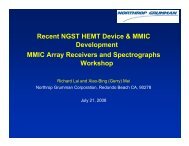
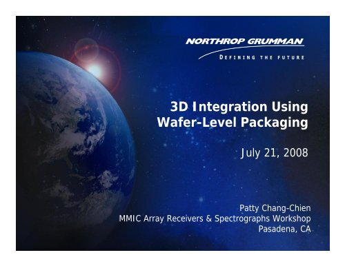
3D Integration Using<br />
Wafer-Level Packaging<br />
July 21, 2008<br />
Patty <strong>Chang</strong>-<strong>Chien</strong><br />
MMIC Array Receivers & Spectrographs Workshop<br />
Pasadena, CA
Agenda<br />
• Wafer-Level Packaging Technology Overview<br />
• IRAD development on large arrays<br />
• Advanced Integration<br />
• Next Level Assembly<br />
• Summary / Future work<br />
2
What is Wafer-Level-Packaging<br />
Wafer-Level Packaging<br />
AKA: Micro Packaging<br />
AKA: Wafer-Scale Assemlby<br />
(WSA)<br />
3<br />
State-of-the-art<br />
MMIC Wafer<br />
• Add inter-cavity interconnects and cavity ring<br />
• Stack and bond multiple wafers, then dice<br />
• Forms a hermetically packaged 3-D integrated circuit<br />
• Enables integration of different MMIC technologies<br />
3-D Wafer Scale<br />
Assembled IC<br />
WLP provides low cost, high volume, hermetic packaging
Integrated Microwave Assembly Packaging<br />
GaAs<br />
GaN<br />
InP<br />
CMOS<br />
IMA<br />
4
Wafer-Level Integration Benefits<br />
• Hermetic<br />
• Ultra-light weight, ultra-compact<br />
• Low cost, high volume<br />
• Performance enhancement<br />
IMAs<br />
Weight: g to >1000g<br />
Size: cm x cm x cm<br />
Assembly: serial, manual<br />
Package near<br />
a thumb tack<br />
Wafer-Level Integrated Package<br />
Weight: < 50 mg<br />
Size: mm x mm x mm<br />
Assembly: mass parallel, wafer scale<br />
5
Superiority And Affordability<br />
• Superiority<br />
– Hermetic packaging in compact form factor<br />
• Protect MMICs against harsh environment<br />
• Enhance circuit reliability<br />
– Superb circuit performance<br />
• Good circuit isolation<br />
• Low transition loss<br />
• Low parasitics: eliminate wire bonds<br />
– High functional density<br />
• One package replaces many MMICs<br />
Size<br />
Weight<br />
Cost<br />
Integrated<br />
Microwave<br />
Assembly<br />
(IMA)<br />
1<br />
1<br />
1<br />
Wafer-Level-<br />
Package (WLP)<br />
1/1000 & ⇓<br />
1/1000 & ⇓<br />
1/100 & ⇓<br />
• Ultra compact, ultra light weight<br />
• Relax system requirement: decrease # of modules required, simple drive scheme<br />
Factors of<br />
Improvement<br />
> 100,000,000<br />
• Affordability<br />
– Batch fabrication processes, low cost, high volume<br />
– Reduce higher order assembly cost, relax module assembly requirement<br />
Heterogeneous Integration Offers Superiority<br />
in Performance and Affordability in Cost<br />
6
2-Layer WLP<br />
• Wafers are individually processed prior to bonding<br />
– No changes to standard MMIC processes<br />
• ICIC = Intra-Cavity InterConnections<br />
2-layer Bonding Process Flow<br />
ICIC<br />
• BICIC = Backside ICIC<br />
2-layer Bonding Process Flow<br />
Wafer 1 Wafer 2<br />
Flip & align<br />
BICIC<br />
ICIC (Front side)<br />
BICIC (backside)<br />
Bonding Layer<br />
Wafer Bonding<br />
Bonded pair<br />
7<br />
2-Layer WLP is Constructed by<br />
Bonding 2 Individually Processed Wafers
Integration Using Wafer-Level Packaging<br />
• WLP is assembled using a low temperature wafer bonding process<br />
• WLP technology is fully compatible with NGST MMIC production<br />
processes<br />
Through<br />
Via<br />
Bonding<br />
Ring<br />
(wafer 1)<br />
Circuit with Wafer Bonding Ring<br />
Wafer<br />
Bonding<br />
Circuit<br />
(low-noise amplifier)<br />
Bonding<br />
Ring<br />
(wafer 2)<br />
Low temperature wafer bonding process is<br />
key to MMIC compatible, robust WLP<br />
8
Examples of Packaged MMICs<br />
Ku Band PA, WLP GaAs HEMT circuit<br />
Ku Band LNA, WLP GaAs HEMT circuit<br />
25<br />
30<br />
20<br />
25<br />
S21 (dB)<br />
15<br />
10<br />
5<br />
S21 (dB)<br />
20<br />
15<br />
10<br />
5<br />
0<br />
5 10 15 20 25<br />
Frequency (GHz)<br />
Q-Band WLP LNA, Q-Band WLP LNA GaAs (IRFFE) HEMT Circuit<br />
0<br />
0 5 10 15 20 25<br />
Frequency (GHz)<br />
W-Band PA, WLP GaAs HEMT circuit<br />
16<br />
20<br />
14<br />
10<br />
12<br />
S21 (dB)<br />
0<br />
-10<br />
-20<br />
LNA<br />
S21 (dB)<br />
10<br />
8<br />
6<br />
4<br />
-30<br />
Bonding Ring<br />
2<br />
9<br />
-40<br />
0 10 20 30 40 50<br />
Frequency (GHz)<br />
0<br />
80 85 90 95 100 105 110<br />
Frequency (GHz)
Comparison of WLP and non-WLP circuits<br />
1.4mm<br />
1.9mm<br />
ALH 140<br />
2.5mm<br />
ALH 140V3 (WLP)<br />
S21 (dB)<br />
18<br />
16<br />
14<br />
12<br />
10<br />
8<br />
6<br />
4<br />
2<br />
ALH140 vs. ALH140V3<br />
: Conventional ALH140<br />
(FIDR1/A-J103 1146A-031)<br />
: ALH140V3 with WLP cover<br />
(WLP5/1/P200-001)<br />
0<br />
30 31 32 33 34 35 36 37 38 39 40<br />
ALH140_1<br />
ALH140_2<br />
ALH140_3<br />
ALH140_4<br />
ALH140_5<br />
ALH140_6<br />
ALH140_7<br />
ALH140_8<br />
ALH140_9<br />
ALH140_10<br />
ALH140_11<br />
ALH140_12<br />
ALH140_V3_1<br />
ALH140_V3_2<br />
ALH140_V3_3<br />
ALH140_V3_4<br />
ALH140_V3_5<br />
ALH140_V3_6<br />
ALH140_V3_7<br />
ALH140_V3_8<br />
ALH140_V3_9<br />
ALH140_V3_10<br />
ALH140_V3_11<br />
ALH140_V3_12<br />
3.2mm<br />
Frequency (GHz)<br />
RF performance similar for WLP and non-WLP circuits<br />
10
Converting Existing Chips to WLP<br />
• Almost all existing chips can be converted into a WLP chip with a<br />
passive cover<br />
• Layout changes are straightforward<br />
• RF performance of converted chip will change depending on chip<br />
sensitivity, performance, and frequency<br />
• Simulations may need to be performed to assess RF performance<br />
changes due to WLP cavity<br />
• WLP conversion will generally increase the size of the chip<br />
11
Heterogeneous Integration Example<br />
• Integrated RF front end module with antenna<br />
– PA (GaAs HEMT)<br />
– 3 bit phase shifter (GaAs HEMT)<br />
– Interconnections (ICICs)<br />
– Antenna<br />
WLP bottom side<br />
Integrated RF Front-End Module<br />
WLP top side<br />
(antenna)<br />
Wafer 1<br />
antenna<br />
Sealing Ring<br />
(Wafer 2)<br />
Wafer<br />
Bonding<br />
Wafer 2<br />
ICIC<br />
Amplifier<br />
Sealing Ring<br />
(Wafer 1)<br />
Phase<br />
shifter<br />
Wafer 1<br />
Ground Fence<br />
Through wafer via<br />
12
WLP Linear Array Demonstration<br />
• Demonstrated fully functional front-end<br />
modules with a linear 4-element array<br />
– GaAs HEMT + passive<br />
– LNA + 3bit PS + antenna in an integrated<br />
Q-Band WLP package<br />
– Successful integration to BFN board<br />
– Demonstrated electronic beam steering<br />
E-Field Magnitude (dB)<br />
0<br />
-5<br />
-10<br />
-15<br />
-20<br />
-25<br />
-30<br />
-35<br />
Measured Beam Pattern<br />
θ= 0°<br />
θ=15°<br />
Integrated RF front-end modules w/ antenna<br />
-40<br />
-60 -40 -20 0 20 40 60<br />
θ (deg)<br />
Beam Forming Network (board)<br />
WLP bottom side<br />
WLP top side<br />
(antenna)<br />
13
WLP Demonstrations<br />
• WLP is fully compatible with NGST’s MMIC production processes<br />
• Demonstrations to-date<br />
– Different compound-semiconductor technologies<br />
w/ WLP<br />
• InP HEMTs<br />
• GaAs HEMTs<br />
• GaAs HBTs<br />
• GaAs Schottky diodes<br />
• InP HBTs<br />
• ABCS HEMT<br />
• MEMS switches<br />
• Passive components<br />
– Frequency bands w/ WLP<br />
• X-band<br />
• Ka-band<br />
• Q-band<br />
• Ku-band<br />
• V-band<br />
• W-band<br />
– Different circuit types w/ WLP<br />
• LNAs<br />
• PAs<br />
• Oscillators<br />
• Phase shifters<br />
• Shift registers<br />
– Substrate combinations w/ WLP<br />
• GaAs + GaAs<br />
• InP + GaAs<br />
• InP + InP<br />
• Quartz + Quartz<br />
• Si + InP<br />
• Glass + Glass<br />
• GaAs x 3<br />
• GaAs x 4<br />
• GaAs x 5<br />
• GaAs + Duroid<br />
• GaAs + InP + GaAs<br />
NGST has extensive experience in heterogeneous integration using WLP<br />
14
Package Integrity<br />
• WLP packages passed the following tests:<br />
• Vibration-Sine<br />
– MIL-STD 883F, Method 2007.3, condition B<br />
• Mechanical Shock (Pyroshock)<br />
– MIL-STD 883F, Method 2002.4, condition B<br />
• Temperature Cycling<br />
– MIL-STD 883F, Method 1010.8, condition B<br />
– -55ºC to 125ºC, 50 cycles, MEMS<br />
– -55ºC to 85ºC, 300+ cycles, W-Band GaAs circuits<br />
• Hermeticity<br />
– MIL-STD 883F, Method 1014.11<br />
– He fine leak, condition A2, flexible<br />
– Radioisotope fine leak, condition B<br />
– Penetrate dye gross leak, condition D<br />
• Die Shear<br />
– MIL-STD 883F, method 2019.7<br />
• Environmental test: 85C 85% humidity 7 days Ku band GaAs MMICs<br />
15<br />
WLP packages are hermetic, thermally<br />
and mechanically robust
Advanced Integration: Multiple Layer WLP<br />
• 4-layer construction<br />
– Use bonded pair as starting units<br />
4-layer Bonding Process Flow<br />
Bonded Pair 1 Bonded Pair 2<br />
Multiple Layer WSA Flow<br />
Bonded Pair 1<br />
Bonded Pair 2<br />
or single wafer<br />
Process Bonding<br />
layer if necessary<br />
(backside)<br />
ICIC (Front side)<br />
BICIC (backside)<br />
Bonding Layer<br />
Wafer Bonding<br />
16<br />
4-Layer Construction is Achieved By<br />
Bonding 2 bonded WLP pairs
X-Band Tri-Layer Tx/Rx Modules<br />
WLP Tx/Rx Module<br />
ABCS HEMT LNA<br />
Average mass: 12.9mg<br />
Size: 2.5mm x 2mm x 0.46mm<br />
17<br />
•Next-Generation Large Aperture<br />
Array T/R Module<br />
–Ultra light weight (10 6 Hours<br />
Switch<br />
Switch<br />
InP HBT PA & digital control<br />
GaAs HEMT PS & Switches<br />
Demonstrated X-Band X<br />
Integrated T/R Module
Microbump: Chip-Board Integration<br />
• Developed microbump technologies for WLP–<br />
to-board attachment and integration<br />
Cu stud microbump<br />
Microbumps on backside of the package<br />
Sn/Pb microbump array<br />
Microbumps Enable WLP-to<br />
to-Board Integration<br />
18
Direct Board Attach Using Microbumps<br />
chip<br />
board<br />
Cu studs<br />
X-ray result showing good board to chip interface<br />
19<br />
Good Chip-to<br />
to-Board<br />
Microbump Interface
Epoxy Attach and Ribbon Bonds<br />
Ku Band subarray board with WLP chips<br />
Integrated Subarray<br />
Antenna Board<br />
Measured Far Field Pattern<br />
5 WLP MMIC fixture<br />
for environmental<br />
testing<br />
Normalized Amplitude<br />
-45.0<br />
-25.0<br />
0.0 25.0 45.0<br />
Azimuth (θ)<br />
20<br />
WLPs are compatible with epoxy attachment
Summary & Future Work<br />
• Demonstrated 100% MMIC compatibility of WLP technology with MMIC<br />
production processes<br />
– Many circuits using different semiconductor technology<br />
• Demonstrated heterogeneous integration using WLP<br />
• Demonstrated robust hermetic WLP packages<br />
• Proven manufacturability (yield and performance)<br />
• Long-term package reliability in progress<br />
• Continue to develop/mature advanced integration technology<br />
• Technology qualification in progress<br />
21