Transient Suppression Products - AVX
Transient Suppression Products - AVX
Transient Suppression Products - AVX

You also want an ePaper? Increase the reach of your titles
YUMPU automatically turns print PDFs into web optimized ePapers that Google loves.
<strong>AVX</strong> <strong>Transient</strong> <strong>Suppression</strong><br />
<strong>Products</strong><br />
<strong>Transient</strong> <strong>Suppression</strong><br />
www.avx.com<br />
Version 14.1
<strong>Transient</strong> <strong>Suppression</strong> <strong>Products</strong><br />
The contents of this catalog are entitled and located on the pages noted below:<br />
TransGuard ® Product Overview . . . . . . . . . . . . . . . . . . . . . . . . . . . . . . . . . . . . . . . . . . . . . . . . . . . . . . . . . . . . . . . . . . . . . . . . . . . . . . . . . . . . . . . . . . . . . . . . . 1<br />
Part Number Identification. . . . . . . . . . . . . . . . . . . . . . . . . . . . . . . . . . . . . . . . . . . . . . . . . . . . . . . . . . . . . . . . . . . . . . . . . . . . . . . . . . . . . . . . . . . . . . . . . . . . . . . . . 2<br />
TransGuard ® Electrical Characteristics . . . . . . . . . . . . . . . . . . . . . . . . . . . . . . . . . . . . . . . . . . . . . . . . . . . . . . . . . . . . . . . . . . . . . . . . . . . . . . . . . 3-4<br />
Dimensions . . . . . . . . . . . . . . . . . . . . . . . . . . . . . . . . . . . . . . . . . . . . . . . . . . . . . . . . . . . . . . . . . . . . . . . . . . . . . . . . . . . . . . . . . . . . . . . . . . . . . . . . . . . . . . . . . . . . . . . . . . . . . . . . . . 5<br />
TransGuard ® Performance Curves . . . . . . . . . . . . . . . . . . . . . . . . . . . . . . . . . . . . . . . . . . . . . . . . . . . . . . . . . . . . . . . . . . . . . . . . . . . . . . . . . . . . . . . 6-10<br />
TransGuard ® Automotive Series . . . . . . . . . . . . . . . . . . . . . . . . . . . . . . . . . . . . . . . . . . . . . . . . . . . . . . . . . . . . . . . . . . . . . . . . . . . . . . . . . . . . . . . . . 11-18<br />
Automotive Sub pF AG Series . . . . . . . . . . . . . . . . . . . . . . . . . . . . . . . . . . . . . . . . . . . . . . . . . . . . . . . . . . . . . . . . . . . . . . . . . . . . . . . . . . . . . . . . . . . . 19-21<br />
Miniature AC Varistor – MAV . . . . . . . . . . . . . . . . . . . . . . . . . . . . . . . . . . . . . . . . . . . . . . . . . . . . . . . . . . . . . . . . . . . . . . . . . . . . . . . . . . . . . . . . . . . . . . 22-24<br />
Radial Leaded High Tempeature Automotive, 150ºC Rated Radial Leaded. . . . . . . . . . . . . . . . . . . 25-26<br />
Controlled Capacitance Multilayer Varistor . . . . . . . . . . . . . . . . . . . . . . . . . . . . . . . . . . . . . . . . . . . . . . . . . . . . . . . . . . . . . . . . . . . . . . 27-28<br />
Miniature 0201 MLV . . . . . . . . . . . . . . . . . . . . . . . . . . . . . . . . . . . . . . . . . . . . . . . . . . . . . . . . . . . . . . . . . . . . . . . . . . . . . . . . . . . . . . . . . . . . . . . . . . . . . . . . . . . . . 29-30<br />
High Temperature Automotive 150ºC Rated Varistors . . . . . . . . . . . . . . . . . . . . . . . . . . . . . . . . . . . . . . . . . . . . . . . . . . . . . 31-32<br />
Glass Encapsulated SMD Varistor MLV. . . . . . . . . . . . . . . . . . . . . . . . . . . . . . . . . . . . . . . . . . . . . . . . . . . . . . . . . . . . . . . . . . . . . . . . . . . . . 33-42<br />
Glass Encapsulated TransGuard ® . . . . . . . . . . . . . . . . . . . . . . . . . . . . . . . . . . . . . . . . . . . . . . . . . . . . . . . . . . . . . . . . . . . . . . . . . . . . . . . . . . . . . . 43-44<br />
Glass Encapsulated TransGuard ® Automotive Series . . . . . . . . . . . . . . . . . . . . . . . . . . . . . . . . . . . . . . . . . . . . . . . . . . . . . . 45-46<br />
StaticGuard . . . . . . . . . . . . . . . . . . . . . . . . . . . . . . . . . . . . . . . . . . . . . . . . . . . . . . . . . . . . . . . . . . . . . . . . . . . . . . . . . . . . . . . . . . . . . . . . . . . . . . . . . . . . . . . . . . . . . . . . . 47-49<br />
StaticGuard Automotive Series . . . . . . . . . . . . . . . . . . . . . . . . . . . . . . . . . . . . . . . . . . . . . . . . . . . . . . . . . . . . . . . . . . . . . . . . . . . . . . . . . . . . . . . . . . 50-52<br />
MultiGuard. . . . . . . . . . . . . . . . . . . . . . . . . . . . . . . . . . . . . . . . . . . . . . . . . . . . . . . . . . . . . . . . . . . . . . . . . . . . . . . . . . . . . . . . . . . . . . . . . . . . . . . . . . . . . . . . . . . . . . . . . . . . 53-56<br />
AntennaGuard 0402/0603 . . . . . . . . . . . . . . . . . . . . . . . . . . . . . . . . . . . . . . . . . . . . . . . . . . . . . . . . . . . . . . . . . . . . . . . . . . . . . . . . . . . . . . . . . . . . . . . . . . . 57-60<br />
AntennaGuard/Sub pF . . . . . . . . . . . . . . . . . . . . . . . . . . . . . . . . . . . . . . . . . . . . . . . . . . . . . . . . . . . . . . . . . . . . . . . . . . . . . . . . . . . . . . . . . . . . . . . . . . . . . . . . 61-62<br />
AntennaGuard Automotive Series . . . . . . . . . . . . . . . . . . . . . . . . . . . . . . . . . . . . . . . . . . . . . . . . . . . . . . . . . . . . . . . . . . . . . . . . . . . . . . . . . . . . . 63-65<br />
USB Series Varistors . . . . . . . . . . . . . . . . . . . . . . . . . . . . . . . . . . . . . . . . . . . . . . . . . . . . . . . . . . . . . . . . . . . . . . . . . . . . . . . . . . . . . . . . . . . . . . . . . . . . . . . . . . . 66-69<br />
Communication BUS Varistors. . . . . . . . . . . . . . . . . . . . . . . . . . . . . . . . . . . . . . . . . . . . . . . . . . . . . . . . . . . . . . . . . . . . . . . . . . . . . . . . . . . . . . . . . . . 70-71<br />
UltraGuard . . . . . . . . . . . . . . . . . . . . . . . . . . . . . . . . . . . . . . . . . . . . . . . . . . . . . . . . . . . . . . . . . . . . . . . . . . . . . . . . . . . . . . . . . . . . . . . . . . . . . . . . . . . . . . . . . . . . . . . . . . . . 72-74<br />
TransFeed and TransFeed Array . . . . . . . . . . . . . . . . . . . . . . . . . . . . . . . . . . . . . . . . . . . . . . . . . . . . . . . . . . . . . . . . . . . . . . . . . . . . . . . . . . . . . . . . 75-82<br />
TransFeed Automotive Series . . . . . . . . . . . . . . . . . . . . . . . . . . . . . . . . . . . . . . . . . . . . . . . . . . . . . . . . . . . . . . . . . . . . . . . . . . . . . . . . . . . . . . . . . . . . 83-88<br />
TransGuard ® Typical Circuits Requiring Protection. . . . . . . . . . . . . . . . . . . . . . . . . . . . . . . . . . . . . . . . . . . . . . . . . . . . . . . . . . 89-94<br />
TransGuard ® Application Notes . . . . . . . . . . . . . . . . . . . . . . . . . . . . . . . . . . . . . . . . . . . . . . . . . . . . . . . . . . . . . . . . . . . . . . . . . . . . . . . . . . . . . . . . 95-110<br />
Packaging - Chips . . . . . . . . . . . . . . . . . . . . . . . . . . . . . . . . . . . . . . . . . . . . . . . . . . . . . . . . . . . . . . . . . . . . . . . . . . . . . . . . . . . . . . . . . . . . . . . . . . . . . . . . . . . 111-114<br />
Packaging - Axial Leads. . . . . . . . . . . . . . . . . . . . . . . . . . . . . . . . . . . . . . . . . . . . . . . . . . . . . . . . . . . . . . . . . . . . . . . . . . . . . . . . . . . . . . . . . . . . . . . . . . . . . . . . . 115<br />
NOTICE: Specifications are subject to change without notice. Contact your nearest <strong>AVX</strong> Sales Office for the latest specifications. All statements, information and<br />
data given herein are believed to be accurate and reliable, but are presented without guarantee, warranty, or responsibility of any kind, expressed or implied.<br />
Statements or suggestions concerning possible use of our products are made without representation or warranty that any such use is free of patent infringement<br />
and are not recommendations to infringe any patent. The user should not assume that all safety measures are indicated or that other measures may not be required.<br />
Specifications are typical and may not apply to all applications.
TransGuard ®<br />
<strong>AVX</strong> Multilayer Ceramic <strong>Transient</strong> Voltage Suppressors<br />
GENERAL DESCRIPTION<br />
The <strong>AVX</strong> TransGuard ® <strong>Transient</strong> Voltage Suppressors (TVS)<br />
with unique high-energy multilayer construction represents<br />
state-of-the-art overvoltage circuit protection. Monolithic<br />
multilayer construction provides protection from voltage<br />
transients caused by ESD, lightning, NEMP, inductive switching,<br />
etc. True surface mount product is provided in EIA<br />
industry standard packages. Thru-hole components are<br />
supplied as conformally coated axial devices.<br />
TRANSGUARD ® DESCRIPTION<br />
TransGuard ® products are zinc oxide (ZnO) based ceramic<br />
semiconductor devices with non-linear voltage-current characteristics<br />
(bi-directional) similar to back-to-back zener diodes.<br />
They have the added advantage of greater current and energy<br />
handling capabilities as well as EMI/RFI attenuation. Devices<br />
are fabricated by a ceramic sintering process that yields a<br />
structure of conductive ZnO grains surrounded by electrically<br />
insulating barriers, creating varistor-like behavior.<br />
<strong>AVX</strong> VG series parts (large case size, high energy) are glass<br />
encapsulated. These parts provide the same high reliability<br />
as traditional VC series parts. The glass encapsulation provides<br />
also enhanced resistance against harsh environment or<br />
process such as acids, salts, chlorite flux.<br />
The number of grain-boundary interfaces between conducting<br />
electrodes determines “Breakdown Voltage” of the<br />
device. High voltage applications such as AC line protection<br />
require many grains between electrodes while low voltage<br />
requires few grains to establish the appropriate breakdown<br />
voltage. Single layer ceramic disc processing proved to be a<br />
viable production method for thick cross section devices<br />
with many grains, but attempts to address low voltage<br />
suppression needs by processing single layer ceramic disc<br />
formulations with huge grain sites has had limited success.<br />
<strong>AVX</strong>, the world leader in the manufacture of multilayer<br />
ceramic capacitors, now offers the low voltage transient<br />
protection marketplace a true multilayer, monolithic surface<br />
mount varistor. Technology leadership in processing<br />
thin dielectric materials and patented processes for<br />
precise ceramic grain growth have yielded superior energy<br />
dissipation in the smallest size. Now a varistor has voltage<br />
characteristics determined by design and not just cell sorting<br />
whatever falls out of the process.<br />
Multilayer ceramic varistors are manufactured by mixing<br />
ceramic powder in an organic binder (slurry) and casting it<br />
into thin layers of precision thickness. Metal electrodes are<br />
deposited onto the green ceramic layers which are then<br />
stacked to form a laminated structure. The metal electrodes<br />
are arranged so that their terminations alternate from one<br />
end of the varistor to the other. The device becomes a<br />
monolithic block during the sintering (firing) cycle providing<br />
uniform energy dissipation in a small volume.<br />
1
TransGuard ®<br />
<strong>AVX</strong> Multilayer Ceramic <strong>Transient</strong> Voltage Suppressors<br />
PART NUMBER IDENTIFICATION<br />
Surface Mount Devices<br />
Axial Leaded Devices<br />
Important: For part number identification only, not for<br />
construction of part numbers.<br />
The information below only defines the numerical value of part number<br />
digits, and cannot be used to construct a desired set of electrical limits.<br />
Please refer to the TransGuard ® part number data for the correct electrical<br />
ratings.<br />
V C 1206 05 D 150 R P<br />
TERMINATION FINISH:<br />
P = Ni/Sn Alloy (Plated)<br />
Important: For part number identification only, not for<br />
construction of part numbers.<br />
The information below only defines the numerical value of part number<br />
digits, and cannot be used to construct a desired set of electrical limits.<br />
Please refer to the TransGuard ® part number data for the correct electrical<br />
ratings.<br />
V A 1000 05 D 150 R<br />
L<br />
LEAD FINISH:<br />
Copper clad steel, solder coated<br />
PACKAGING (Pcs/Reel):<br />
STYLE “D” “R” “T” “W”<br />
VC0402 N/A N/A N/A 10,000<br />
VC0603 1,000 4,000 10,000 N/A<br />
VC0805 1,000 4,000 10,000 N/A<br />
VC1206 1,000 4,000 10,000 N/A<br />
VC1210 1,000 2,000 10,000 N/A<br />
CLAMPING VOLTAGE:<br />
Where: 100 = 12V 500 = 50V<br />
150 = 18V 560 = 60V<br />
200 = 22V 580 = 60V<br />
250 = 27V 620 = 67V<br />
300 = 32V 650 = 67V<br />
390 = 42V 101 = 100V<br />
400 = 42V 121 = 120V<br />
ENERGY:<br />
Where: A = 0.1J J = 1.5J S = 1.9-2.0J<br />
B = 0.2J K = 0.6J T = 0.01J<br />
C = 0.3J L = 0.8J U = 4.0-5.0J<br />
D = 0.4J M = 1.0J V = 0.02J<br />
E = 0.5J N = 1.1J W = 6.0J<br />
F = 0.7J P = 3.0J X = 0.05J<br />
G = 0.9J Q = 1.3J Y = 12.0J<br />
H = 1.2J R = 1.7J Z = 25.0J<br />
WORKING VOLTAGE:<br />
Where: 03 = 3.3 VDC 18 = 18.0 VDC<br />
05 = 5.6 VDC 26 = 26.0 VDC<br />
09 = 9.0 VDC 30 = 30.0 VDC<br />
12 = 12.0 VDC 48 = 48.0 VDC<br />
14 = 14.0 VDC 60 = 60.0 VDC<br />
85 = 85.0 VDC<br />
CASE SIZE DESIGNATOR:<br />
SIZE LENGTH WIDTH<br />
0402 1.00±0.10mm (0.040"±0.004") 0.5±0.10mm (0.020"±0.004")<br />
0603 1.60±0.15mm (0.063"±0.006") 0.8±0.15mm (0.032"±0.006")<br />
0805 2.01±0.2mm (0.079"±0.008") 1.25±0.2mm (0.049"±0.008")<br />
1206 3.20±0.2mm (0.126"±0.008") 1.60±0.2mm (0.063"±0.008")<br />
1210 3.20±0.2mm (0.126"±0.008") 2.49±0.2mm (0.098"±0.008")<br />
CASE STYLE:<br />
C = Chip<br />
G = Chip Glass Encapsulated<br />
PRODUCT DESIGNATOR:<br />
V = Varistor<br />
MARKING:<br />
All standard surface mount TransGuard ® chips will not be marked.<br />
PACKAGING (Pcs/Reel):<br />
STYLE “D” “R” “T”<br />
VA1000 1,000 3,000 7,500<br />
VA2000 1,000 2,500 5,000<br />
CLAMPING VOLTAGE:<br />
Where: 100 = 12V 580 = 60V<br />
150 = 18V 650 = 67V<br />
300 = 32V 101 = 100V<br />
400 = 42V 121 = 120V<br />
ENERGY:<br />
Where: A = 0.1J<br />
D = 0.4J<br />
K = 2.0J<br />
WORKING VOLTAGE:<br />
Where: 03 = 3.3 VDC 26 = 26.0 VDC<br />
05 = 5.6 VDC 30 = 30.0 VDC<br />
14 = 14.0 VDC 48 = 48.0 VDC<br />
18 = 18.0 VDC 60 = 60.0 VDC<br />
CASE SIZE DESIGNATOR:<br />
SIZE LENGTH DIAMETER<br />
1000 4.32mm (0.170") 2.54mm (0.100")<br />
2000 4.83mm (0.190") 3.56mm (0.140")<br />
CASE STYLE:<br />
A = Axial<br />
PRODUCT DESIGNATOR:<br />
V = Varistor<br />
MARKING:<br />
All axial TransGuards ® are marked with vendor identification, product<br />
identification, voltage/energy rating code and date code (see example below):<br />
Where:<br />
<strong>AVX</strong><br />
TVS<br />
05D<br />
825<br />
<strong>AVX</strong> = Always <strong>AVX</strong> (Vendor Identification)<br />
TVS = Always TVS (Product Identification<br />
- <strong>Transient</strong> Voltage Suppressor)<br />
05D = Working VDC and Energy Rating (Joules)<br />
Where: 05 = 5.6 VDC, D = 0.4J<br />
725 = Three Digit Date Code<br />
Where: 8 = Last digit of year (2008)<br />
25 = Week of year<br />
Not RoHS Compliant<br />
LEAD-FREE COMPATIBLE<br />
COMPONENT<br />
2<br />
For RoHS compliant products,<br />
please select correct termination style.
TransGuard ®<br />
<strong>AVX</strong> Multilayer Ceramic <strong>Transient</strong> Voltage Suppressors<br />
ELECTRICAL CHARACTERISTICS<br />
<strong>AVX</strong> PN V W (DC) V W (AC) V B V C I VC I L E T I P Cap Freq Case<br />
VC060303A100 3.3 2.3 5.0±20% 12 1 100 0.1 30 1450 K 0603<br />
VC080503A100 3.3 2.3 5.0±20% 12 1 100 0.1 40 1400 K 0805<br />
VC080503C100 3.3 2.3 5.0±20% 12 1 100 0.3 120 5000 K 0805<br />
VC120603A100 3.3 2.3 5.0±20% 12 1 100 0.1 40 1250 K 1206<br />
VC120603D100 3.3 2.3 5.0±20% 12 1 100 0.4 150 4700 K 1206<br />
VA100003A100 3.3 2.3 5.0±20% 12 1 100 0.1 40 1500 K 1000<br />
VA100003D100 3.3 2.3 5.0±20% 12 1 100 0.4 150 4700 K 1000<br />
VC040205X150 5.6 4.0 8.5±20% 18 1 35 0.05 20 175 M 0402<br />
VC060305A150 5.6 4.0 8.5±20% 18 1 35 0.1 30 750 K 0603<br />
VC080505A150 5.6 4.0 8.5±20% 18 1 35 0.1 40 1100 K 0805<br />
VC080505C150 5.6 4.0 8.5±20% 18 1 35 0.3 120 3000 K 0805<br />
VC120605A150 5.6 4.0 8.5±20% 18 1 35 0.1 40 1200 K 1206<br />
VC120605D150 5.6 4.0 8.5±20% 18 1 35 0.4 150 3000 K 1206<br />
VA100005A150 5.6 4.0 8.5±20% 18 1 35 0.1 40 1000 K 1000<br />
VA100005D150 5.6 4.0 8.5±20% 18 1 35 0.4 150 2800 K 1000<br />
VC040209X200 9.0 6.4 12.7±15% 22 1 25 0.05 20 175 M 0402<br />
VC060309A200 9.0 6.4 12.7±15% 22 1 25 0.1 30 550 K 0603<br />
VC080509A200 9.0 6.4 12.7±15% 22 1 25 0.1 40 750 K 0805<br />
VC080512A250 12.0 8.5 16±15% 27 1 25 0.1 40 525 K 0805<br />
VC040214X300 14.0 10.0 18.5±12% 32 1 15 0.05 20 85 K 0402<br />
VC060314A300 14.0 10.0 18.5±12% 32 1 15 0.1 30 350 K 0603<br />
VC080514A300 14.0 10.0 18.5±12% 32 1 15 0.1 40 325 K 0805<br />
VC080514C300 14.0 10.0 18.5±12% 32 1 15 0.3 120 900 K 0805<br />
VC120614A300 14.0 10.0 18.5±12% 32 1 15 0.1 40 600 K 1206<br />
VC120614D300 14.0 10.0 18.5±12% 32 1 15 0.4 150 1050 K 1206<br />
VA100014A300 14.0 10.0 18.5±12% 32 1 15 0.1 40 325 K 1000<br />
VA100014D300 14.0 10.0 18.5±12% 32 1 15 0.4 150 1100 K 1000<br />
VC121016J390 16.0 13.0 25.5±10% 40 2.5 10 1.6 500 3100 K 1210<br />
VG181216P400 16.0 11.0 24.5±10% 42 5 10 2.9 1000 5000 K 1812<br />
VG222016Y400 16.0 11.0 24.5±10% 42 10 10 7.2 1500 13000 K 2220<br />
VC040218X400 18.0 13.0 25.5±10% 42 1 10 0.05 20 65 M 0402<br />
VC060318A400 18.0 13.0 25.5±10% 42 1 10 0.1 30 150 K 0603<br />
VC080518A400 18.0 13.0 25.5±10% 42 1 10 0.1 30 225 K 0805<br />
VC080518C400 18.0 13.0 25.5±10% 42 1 10 0.3 100 550 K 0805<br />
VC120618A400 18.0 13.0 25.5±10% 42 1 10 0.1 30 350 K 1206<br />
VC120618D400 18.0 13.0 25.5±10% 42 1 10 0.4 150 900 K 1206<br />
VC120618E380 18.0 13.0 25.5±10% 38 1 15 0.5 200 930 K 1206<br />
VC121018J390 18.0 13.0 25.5±10% 42 5 10 1.6 500 3100 K 1210<br />
VA100018A400 18.0 13.0 25.5±10% 42 1 10 0.1 40 350 K 1000<br />
VA100018D400 18.0 13.0 25.5±10% 42 1 10 0.4 150 900 K 1000<br />
VG121022R440 22.0 17.0 27±10% 44 2.5 10 1.7 400 1600 K 1210<br />
VC060326A580 26.0 18.0 34.5±10% 60 1 10 0.1 30 155 K 0603<br />
VC080526A580 26.0 18.0 34.5±10% 60 1 10 0.1 30 120 K 0805<br />
VC080526C580 26.0 18.0 34.5±10% 60 1 10 0.3 100 250 K 0805<br />
3
TransGuard ®<br />
<strong>AVX</strong> Multilayer Ceramic <strong>Transient</strong> Voltage Suppressors<br />
ELECTRICAL CHARACTERISTICS<br />
<strong>AVX</strong> PN V W (DC) V W (AC) V B V C I VC I L E T I P Cap Freq Case<br />
VC120626D580 26.0 18.0 34.5±10% 60 1 10 0.4 120 500 K 1206<br />
VC120626F540 26.0 20.0 33.0±10% 54 1 15 0.7 200 600 K 1206<br />
VC121026H560 26.0 18.0 34.5±10% 60 5 10 1.2 300 2150 K 1210<br />
VC181226P540 26.0 20.0 33.0±10% 54 5 15 3.0 800 3000 K 1812<br />
VA100026D580 26.0 18.0 34.5±10% 60 1 10 0.4 120 650 K 1000<br />
VC060330A650 30.0 21.0 41.0±10% 67 1 10 0.1 30 125 K 0603<br />
VC080530A650 30.0 21.0 41.0±10% 67 1 10 0.1 30 90 M 0805<br />
VC080530C650 30.0 21.0 41.0±10% 67 1 10 0.3 80 250 K 0805<br />
VC120630D650 30.0 21.0 41.0±10% 67 1 10 0.4 120 400 K 1206<br />
VC121030G620 30.0 21.0 41.0±10% 67 5 10 0.9 220 1750 K 1210<br />
VC121030H620 30.0 21.0 41.0±10% 67 5 10 1.2 280 1850 K 1210<br />
VC121030S620 30.0 21.0 41.0±10% 67 5 10 1.9 300 1500 K 1210<br />
VA100030D650 30.0 21.0 41.0±10% 67 1 10 0.4 120 550 K 1000<br />
VC080531C650 31.0 25.0 39.0±10% 65 1 10 0.3 80 250 K 0805<br />
VC120631M650 31.0 25.0 39.0±10% 65 1 15 1.0 200 500 K 1206<br />
VC080538C770 38.0 30.0 47.0±10% 77 1 10 0.3 80 200 K 0805<br />
VC120638N770 38.0 30.0 47.0±10% 77 1 15 1.1 200 400 K 1206<br />
VG121038S770 38.0 30.0 47.0±10% 77 2.5 15 2.0 400 1000 K 1210<br />
VG181238U770 38.0 30.0 47.0±10% 77 5 15 4.2 800 1300 K 1812<br />
VG222038Y770 38.0 30.0 47.0±10% 77 10 15 12 2000 4200 K 2220<br />
VC120642L800 42.0 32.0 51.0±10% 80 1 15 0.8 180 600 K 1206<br />
VC120645K900 45.0 35.0 56.0±10% 90 1 15 0.6 200 260 K 1206<br />
VC181245U900 45.0 35.0 56.0±10% 90 5 15 4.0 500 1200 K 1812<br />
VC120648D101 48.0 34.0 62.0±10% 100 1 10 0.4 100 225 K 1206<br />
VC121048G101 48.0 34.0 62.0±10% 100 5 10 0.9 220 450 K 1210<br />
VC121048H101 48.0 34.0 62.0±10% 100 5 10 1.2 250 500 K 1210<br />
VA100048D101 48.0 34.0 62.0±10% 100 1 10 0.4 100 200 K 1000<br />
VC120656F111 56.0 40.0 68.0±10% 110 1 15 0.7 100 180 K 1206<br />
VC181256U111 56.0 40.0 68.0±10% 110 5 15 4.8 500 800 K 1812<br />
VC121060J121 60.0 42.0 76.0±10% 120 5 10 1.5 250 400 K 1210<br />
VA200060K121 60.0 42.0 76.0±10% 120 1 10 2.0 300 400 K 2000<br />
VC120665L131 65.0 50.0 82.0±10% 135 1 15 0.8 100 250 K 1206<br />
VC120665M131 65.0 50.0 82.0±10% 135 1 15 1.0 150 250 K 1206<br />
VG121065P131 65.0 50.0 82±10% 135 2.5 15 2.7 350 600 K 1210<br />
VC121085S151 85.0 60.0 100±10% 150 1 35 2.0 250 275 K 1210<br />
V W (DC) DC Working Voltage (V)<br />
V W (AC) AC Working Voltage (V)<br />
V B Typical Breakdown Voltage (V @ 1mA DC )<br />
V B Tol V B Tolerance is ± from Typical Value<br />
V C Clamping Voltage (V @ I VC )<br />
I VC Test Current for V C (A, 8x20μS)<br />
I L Maximum Leakage Current at the<br />
E T<br />
I P<br />
Cap<br />
Freq<br />
Working Voltage (μA)<br />
<strong>Transient</strong> Energy Rating (J, 10x1000μS)<br />
Peak Current Rating (A, 8x20μS)<br />
Typical Capacitance (pF) @ frequency specified<br />
and 0.5 V RMS<br />
Frequency at which capacitance is measured<br />
(K = 1kHz, M = 1MHz)<br />
4
Dimensions<br />
Dimensions: Millimeters<br />
(Inches)<br />
D<br />
Max.<br />
0.51 ±0.05<br />
(0.020" ±0.002")<br />
L<br />
Max.<br />
25.4 (1.0")<br />
Min. Lead Length<br />
DIMENSIONS: mm (inches)<br />
(L) Max Length<br />
<strong>AVX</strong> Style VA1000 VA2000<br />
(D) Max Diameter<br />
Lead Finish: Copper Clad Steel, Solder Coated<br />
mm 4.32 4.83<br />
(in.) (0.170) (0.190)<br />
mm 2.54 3.56<br />
(in.) (0.100) (0.140)<br />
<br />
L<br />
<br />
<br />
W<br />
<br />
<br />
<br />
T<br />
<br />
<br />
t<br />
DIMENSIONS: mm (inches)<br />
(L) Length<br />
(W) Width<br />
<strong>AVX</strong> Style 0402 0603 0805 1206 1210 1812 2220<br />
(T) Max Thickness<br />
(t) Land Length<br />
mm 1.00±0.10 1.60±0.15 2.01±0.20 3.20±0.20 3.20±0.20 4.50±0.30 5.70±0.40<br />
(in.) (0.040±0.004) (0.063±0.006) (0.079±0.008) (0.126±0.008) (0.126±0.008) (0.177±0.012) (0.224±0.016)<br />
mm 0.50±0.10 0.80±0.15 1.25±0.20 1.60±0.20 2.49±0.20 3.20±0.30 5.00±0.40<br />
(in.) (0.020±0.004) (0.031±0.006) (0.049±0.008) (0.063±0.008) (0.098±0.008) (0.126±0.012) (0.197±0.016)<br />
mm 0.6 0.9 1.02 1.02 1.70 2.00 2.50<br />
(in.) (0.024) (0.035) (0.040) (0.040) (0.067) (0.080) (0.098)<br />
mm 0.25±0.15 0.35±0.15 0.71 max. 0.94 max. 1.14 max. 1.00 max. 1.00 max.<br />
(in.) (0.010±0.006) (0.014±0.006) (0.028 max.) (0.037 max.) (0.045 max.) (0.039 max.) (0.039 max.)<br />
5
TransGuard ®<br />
<strong>AVX</strong> Multilayer Ceramic <strong>Transient</strong> Voltage Suppressors<br />
TYPICAL PERFORMANCE CURVES (0402 CHIP SIZE)<br />
VOLTAGE/CURRENT CHARACTERISTICS<br />
Multilayer construction and improved grain structure result in<br />
excellent transient clamping characteristics up to 20 amps<br />
peak current, while maintaining very low leakage currents<br />
under DC operating conditions. The VI curves below show the<br />
voltage/current characteristics for the 5.6V, 9V, 14V, 18V and<br />
low capacitance StaticGuard parts with currents ranging from<br />
parts of a micro amp to tens of amps.<br />
Voltage (V)<br />
100<br />
80<br />
60<br />
40<br />
VC04LC18V500<br />
VC040218X400<br />
VC040214X300<br />
VC040209X200<br />
VC040205X150<br />
PULSE DEGRADATION<br />
Traditionally varistors have suffered degradation of electrical<br />
performance with repeated high current pulses resulting in<br />
decreased breakdown voltage and increased leakage current.<br />
It has been suggested that irregular intergranular<br />
boundaries and bulk material result in restricted current<br />
paths and other non-Schottky barrier paralleled conduction<br />
paths in the ceramic. Repeated pulsing of TransGuard ® transient<br />
voltage suppressors with 150Amp peak 8 x 20μS<br />
waveforms shows negligible degradation in breakdown<br />
voltage and minimal increases in leakage current. This<br />
does not mean that TransGuard ® suppressors do not suffer<br />
degradation, but it occurs at much higher current.<br />
ESD TEST OF 0402 PARTS<br />
35<br />
30<br />
VC04LC18V500<br />
20<br />
0<br />
10 -9 10 -7 10 -5 10 -3 10 -1 10 10 3 10 5<br />
1300<br />
Current (A)<br />
PEAK POWER VS PULSE DURATION<br />
BREAKDOWN VOLTAGE (Vb)<br />
25<br />
20<br />
15<br />
10<br />
VC040218X400<br />
VC040214X300<br />
VC040209X200<br />
VC040205X150<br />
PEAK POWER (W)<br />
1200<br />
1100<br />
1000<br />
900<br />
800<br />
700<br />
600<br />
500<br />
VC040218X400<br />
VC040214X300<br />
VC040209X200<br />
VC04LC18V500<br />
VC040205X150<br />
0<br />
-5<br />
-10<br />
5<br />
10 100 1000 10000<br />
8kV ESD STRIKES<br />
INSERTION LOSS CHARACTERISTICS<br />
400<br />
300<br />
200<br />
100<br />
dB<br />
VC04LC18V<br />
VC040218X<br />
-15<br />
VC040214X<br />
VC040209X<br />
VC040205X<br />
-20<br />
0<br />
10 100 1000<br />
IMPULSE DURATION (μS)<br />
-25<br />
0.01 0.1 1 10<br />
Frequency (GHz)<br />
6
TransGuard ®<br />
<strong>AVX</strong> Multilayer Ceramic <strong>Transient</strong> Voltage Suppressors<br />
TYPICAL PERFORMANCE CURVES (0603, 0805, 1206 & 1210 CHIP SIZES)<br />
VOLTAGE/CURRENT CHARACTERISTICS<br />
Multilayer construction and improved grain structure result in excellent transient clamping characteristics up to 500 amps peak<br />
current, depending on case size and energy rating, while maintaining very low leakage currents under DC operating conditions.<br />
The VI curve below shows the voltage/current characteristics for the 3.3V, 5.6V, 12V, 14V, 18V, 26V, 30V, 48V and<br />
60VDC parts with currents ranging from parts of a micro amp to tens of amps.<br />
25<br />
VI Curves - 3.3V and 5.6V <strong>Products</strong><br />
20<br />
Voltage (V)<br />
15<br />
10<br />
5<br />
50<br />
VI Curves - 9V, 12V, and 14V <strong>Products</strong><br />
0<br />
10 -9 10-6 10-3 10+0 10+3<br />
Current (A)<br />
40<br />
3.3V, 0.1J 3.3V, >0.1J 5.6V, 0.1J 5.6V, >0.1J<br />
Voltage (V)<br />
30<br />
20<br />
10<br />
100<br />
80<br />
VI Curves - 18V and 26V <strong>Products</strong><br />
0<br />
10 -9 10-6 10-3 10+0 10+3<br />
Current (A)<br />
9V, 0.1J 12V, 0.1J 14V, 0.1J 14V, >0.1J<br />
Voltage (V)<br />
60<br />
40<br />
20<br />
200<br />
VI Curves - 30V, 48V, and 60V <strong>Products</strong><br />
0<br />
10 -9 10-6 10-3 10+0 10+3<br />
Current (A)<br />
150<br />
18V, 0.1J 18V, >0.1J 26V, 0.1J 26V, >0.1J<br />
Voltage (V)<br />
100<br />
200<br />
VI Curve - 85V Product<br />
50<br />
160<br />
0<br />
10 -9 10-6 10-3 10+0 10+3<br />
Voltage (V)<br />
120<br />
80<br />
Current (A)<br />
30V, 0.1J 30V, >0.1J 48V 60V<br />
40<br />
0<br />
1.E-09 1.E-06 1.E-03 1.E+00 1.E+03<br />
Current (A)<br />
7
TransGuard ®<br />
<strong>AVX</strong> Multilayer Ceramic <strong>Transient</strong> Voltage Suppressors<br />
TYPICAL PERFORMANCE CURVES (0603, 0805, 1206 & 1210 CHIP SIZES)<br />
3.3V<br />
8
TransGuard ®<br />
<strong>AVX</strong> Multilayer Ceramic <strong>Transient</strong> Voltage Suppressors<br />
TYPICAL PERFORMANCE CURVES (0603, 0805, 1206 & 1210 CHIP SIZES)<br />
TEMPERATURE CHARACTERISTICS<br />
TransGuard ® suppressors are designed to operate over the full temperature range from -55°C to +125°C. This operating<br />
temperature range is for both surface mount and axial leaded products.<br />
Voltage as a Percent of<br />
Average Breakdown Voltage<br />
100<br />
90<br />
80<br />
70<br />
60<br />
50<br />
40<br />
30<br />
20<br />
Temperature Dependence of Voltage<br />
10<br />
10-9 10-8 10-7 10-6 10-5 10-4 10-3 10-2<br />
Current (A)<br />
-40 C 25 C 85 C 125 C<br />
Energy Derating<br />
TYPICAL ENERGY DERATING VS TEMPERATURE<br />
1.25<br />
1<br />
0.8<br />
0.6<br />
0.4<br />
Typical Breakdown (V B )<br />
and Clamping (V C ) Voltages<br />
20<br />
15<br />
10<br />
TYPICAL BREAKDOWN AND CLAMPING VOLTAGES<br />
VS TEMPERATURE - 5.6V<br />
5.6V<br />
5<br />
-55 -40 -20 0 20 40 60 80 100 120 140 150<br />
o<br />
Temperature ( C)<br />
VC<br />
V B<br />
0.2 <br />
0<br />
-60 -40 -20 0 20 40 60 80 100 120 140 160<br />
o<br />
Temperature ( C)<br />
Typical Breakdown (V B )<br />
and Clamping (V C ) Voltages<br />
Typical Breakdown (V B )<br />
and Clamping (V C ) Voltages<br />
50<br />
40<br />
30<br />
TYPICAL BREAKDOWN AND CLAMPING VOLTAGES<br />
VS TEMPERATURE - 18V<br />
18V<br />
( VC<br />
)<br />
( V B )<br />
20<br />
-55 -40 -20 0 20 40 60 80 100 120 140 150<br />
o<br />
Temperature ( C)<br />
60<br />
50<br />
40<br />
TYPICAL BREAKDOWN AND CLAMPING VOLTAGES<br />
VS TEMPERATURE - 26V<br />
26V<br />
( V ) C<br />
( V B )<br />
30<br />
-55 -40 -20 0 20 40 60 80 100 120 140 150<br />
Temperature (∞C)<br />
Capacitance Relative to 25°C<br />
+25<br />
+20<br />
+15<br />
+10<br />
+5<br />
0<br />
-5<br />
-10<br />
-15<br />
-20<br />
TYPICAL CAPACITANCE VS TEMPERATURE<br />
25° C Reference<br />
Average<br />
-25<br />
-40 -20 0 20 40 60 80 100 120 140<br />
Temperature (°C)<br />
9
TransGuard ®<br />
<strong>AVX</strong> Multilayer Ceramic <strong>Transient</strong> Voltage Suppressors<br />
TYPICAL PERFORMANCE CURVES (0603, 0805, 1206 & 1210 CHIP SIZES)<br />
PULSE DEGRADATION<br />
Traditionally varistors have suffered degradation of electrical performance<br />
with repeated high current pulses resulting in decreased<br />
breakdown voltage and increased leakage current. It has been<br />
suggested that irregular intergranular boundaries and bulk material<br />
result in restricted current paths and other non-Schottky barrier<br />
paralleled conduction paths in the ceramic. Repeated pulsing of<br />
both 5.6 and 14V TransGuard ® transient voltage suppressors with<br />
150 Amp peak 8 x 20μS waveforms shows negligible degradation<br />
in breakdown voltage and minimal increases in leakage current.<br />
This does not mean that TransGuard ® suppressors do not suffer<br />
degradation, but it occurs at much higher current. The plots<br />
of typical breakdown voltage vs number of 150A pulses are<br />
shown below.<br />
Change in Breakdown Voltage (%)<br />
Change in Breakdown Voltage (%)<br />
10%<br />
8%<br />
6%<br />
4%<br />
2%<br />
0%<br />
0 100 200 300 400 500 600<br />
Number of Strikes<br />
Figure 1<br />
VC120618D400<br />
VC120626D580<br />
VC120614D300<br />
VC120605D150<br />
Repetitive Peak Current Strikes<br />
TransGuard ® 0805 0.1J and 0.3J <strong>Products</strong><br />
15%<br />
10%<br />
5%<br />
0%<br />
Repetitive Peak Current Strikes<br />
TransGuard ® 1206 0.4J Product<br />
0 100 200 300 400 500 600<br />
Number of Strikes<br />
Figure 2<br />
VC080518A400<br />
VC080518C400<br />
Change in Breakdown Voltage (%)<br />
Change in Breakdown Voltage (%)<br />
Repetitive Peak Current Strikes<br />
TransGuard ® 1210 1.5J Product<br />
10%<br />
8%<br />
6%<br />
4%<br />
2%<br />
0%<br />
30%<br />
25%<br />
20%<br />
15%<br />
10%<br />
5%<br />
0%<br />
VC121018J390<br />
0 100 200 300 400 500 600<br />
Number of Strikes<br />
Figure 3<br />
Repetitive Peak Current Strikes<br />
StaticGuard 0805 0.1J Product<br />
VC08LC18A500<br />
0 100 200 300 400 500 600<br />
Number of Strikes<br />
Figure 4<br />
CAPACITANCE/FREQUENCY<br />
CHARACTERISTICS<br />
TransGuard ® Capacitance vs Frequency 0603 TransGuard ® Capacitance vs Frequency 0805 TransGuard ® Capacitance vs Frequency 1206<br />
100<br />
100<br />
100<br />
Capacitance Change (%)<br />
80<br />
60<br />
40<br />
20<br />
VC060305A150<br />
VC06LC18X500<br />
0<br />
VC060326A580<br />
0 20 40 60 80 100<br />
Frequency (MHz)<br />
Capacitance Change (%)<br />
80<br />
60<br />
40<br />
VC080505C150<br />
20<br />
VC080518C400<br />
0<br />
VC080514A300<br />
0 20 40 60 80 100<br />
Frequency (MHz)<br />
Capacitance Change (%)<br />
80<br />
60<br />
40<br />
20<br />
VC120614D300<br />
VC120648D101<br />
0<br />
VC12LC18A500<br />
0 20 40 60 80 100<br />
Frequency (MHz)<br />
10
TransGuard ® Automotive Series<br />
Multilayer Varistors for Automotive Applications<br />
GENERAL DESCRIPTION<br />
The TransGuard Automotive Series are zinc oxide (ZnO) based ceramic semiconductor<br />
devices with non-linear, bi-directional voltage-current characteristics.<br />
They have the advantage of offering bi-directional overvoltage protection as well as<br />
EMI/RFI attenuation in a single SMT package. The Automotive Series high current<br />
and high energy handling capability make them well suited for protection against<br />
automotive related transients.<br />
<strong>AVX</strong> VG series parts (large case size, high energy) are glass encapsulated. These<br />
parts provide the same high reliability as traditional VC series parts. The glass<br />
encapsulation provides also enhanced resistance against harsh environment or<br />
process such as acids, salts, chlorite flux.<br />
Operating Temperature: -55ºC to +125ºC<br />
LEAD-FREE COMPATIBLE<br />
COMPONENT<br />
FEATURES<br />
• High Reliability<br />
• High Energy Absorption (Load Dump)<br />
• High Current Handling<br />
• AEC Q200 Qualified<br />
• Bi-Directional protection<br />
• EMI/RFI attenuation<br />
• Multi-strike capability<br />
• Sub 1nS response to ESD strike<br />
APPLICATIONS<br />
• Internal Combustion Engine (ICE) Vehicles<br />
• Hybrid Electric Vehicles (HEV)<br />
• Plug-in Hybrid Electric Vehicles (PHEV)<br />
• Commercial Vehicles<br />
– CAN, LIN, FLEXRAY based modules<br />
– Sensors<br />
– Module load dump protection<br />
– Motor/inductive load transient suppression<br />
HOW TO ORDER<br />
VC<br />
AS<br />
1206<br />
18<br />
D<br />
400<br />
R<br />
P<br />
Varistor Chip<br />
VC = Varistor Chip<br />
VG = Varistor Glass<br />
Encapsulated<br />
Chip<br />
*Not available for 0402<br />
**Only available for 0402<br />
Automotive<br />
Series<br />
Case<br />
Size<br />
0402<br />
0603<br />
0805<br />
1206<br />
1210<br />
1812<br />
2220<br />
05 = 5.6Vdc<br />
09 = 9Vdc<br />
12 = 12Vdc<br />
14 = 14Vdc<br />
16 = 16Vdc<br />
18 = 18Vdc<br />
26 = 26Vdc<br />
30 = 30Vdc<br />
31 = 31Vdc<br />
Working<br />
Voltage<br />
34 = 34Vdc<br />
38 = 38Vdc<br />
42 = 42Vdc<br />
45 = 45Vdc<br />
48 = 48Vdc<br />
56 = 56Vdc<br />
60 = 60Vdc<br />
85 = 85Vdc<br />
A = 0.1J<br />
B = 0.2J<br />
C = 0.3J<br />
D = 0.4J<br />
E = 0.5J<br />
F = 0.7J<br />
H = 1.2J<br />
J = 1.5J<br />
K = 0.6J<br />
Energy<br />
Rating<br />
L = 0.8J<br />
S = 1.9-2.0J<br />
X = 0.05J<br />
M = 1J<br />
N = 1.1J<br />
U = 4.0-5.0J<br />
P = 2.7-3.0J<br />
Y = 7.2-12J<br />
150 = 18V<br />
220 = 22V<br />
250 = 27V<br />
300 = 32V<br />
380 = 38V<br />
390 = 42V<br />
400 = 42V<br />
540 = 54V<br />
Clamping<br />
Voltage<br />
580 = 60V<br />
620 = 67V<br />
650 = 67V<br />
770 = 77V<br />
800 = 80V<br />
101 = 100V<br />
111 = 110V<br />
151 = 150V<br />
Package<br />
D = 7" (1000)*<br />
R = 7" (4000)*<br />
T = 13" (10,000)*<br />
W = 13" (10,000)**<br />
0402 only<br />
Termination<br />
P = Ni/Sn plated<br />
PHYSICAL DIMENSIONS: mm (inches)<br />
T<br />
W<br />
t<br />
L<br />
t<br />
Size (EIA) Length (L) Width (W) Max Thickness (T) Land Length (t)<br />
1.00±0.10 0.50±0.10 0.60 0.25±0.15<br />
0402<br />
(0.040±0.004) (0.020±0.004) (0.024) (0.010±0.006)<br />
0603<br />
0805<br />
1206<br />
1210<br />
1812<br />
2220<br />
1.60±0.15 0.80±0.15 0.90 0.35±0.15<br />
(0.063±0.006) (0.031±0.006) (0.035) (0.014±0.006)<br />
2.01±0.20 1.25±0.20 1.02 0.71 max.<br />
(0.079±0.008) (0.049±0.008) (0.040) (0.028 max.)<br />
3.20±0.20 1.60±0.20 1.02 0.94 max.<br />
(0.126±0.008) (0.063±0.008) (0.040) (0.037 max.)<br />
3.20±0.20 2.49±0.20 1.70 0.14 max.<br />
(0.126±0.008) (0.098±0.008) (0.067) (0.045 max.)<br />
4.50±0.30 3.20±0.30 2.00 1.00 max.<br />
(0.177±0.012) (0.126±0.012) (0.079) (0.040 max.)<br />
5.70±0.40 5.00±0.40 2.50 1.00 max.<br />
(0.224±0.016) (0.197±0.016) (0.098) (0.040 max.)<br />
11
TransGuard ® Automotive Series<br />
Multilayer Varistors for Automotive Applications<br />
ELECTRICAL CHARACTERISTICS<br />
<strong>AVX</strong> PN V W (DC) V W (AC) V B V C I VC I L E T E LD I P Cap Freq V Jump P Diss. Max<br />
VCAS040205X150 _ _ 5.6 4.0 8.5±20% 18 1 35 0.05 - 20 175 M - 0.001<br />
VCAS060305A150 _ _ 5.6 4.0 8.5±20% 18 1 35 0.1 - 30 750 K - 0.001<br />
VCAS080505A150 _ _ 5.6 4.0 8.5±20% 18 1 35 0.1 - 40 1100 K - 0.001<br />
VCAS080505C150 _ _ 5.6 4.0 8.5±20% 18 1 35 0.3 - 120 3000 K - 0.005<br />
VCAS120605A150 _ _ 5.6 4.0 8.5±20% 18 1 35 0.1 - 40 1200 K - 0.002<br />
VCAS120605D150 _ _ 5.6 4.0 8.5±20% 18 1 35 0.4 - 150 3000 K - 0.008<br />
VCAS040209X200 _ _ 9 6.4 12.7±15% 22 1 25 0.05 - 20 175 M - 0.001<br />
VCAS060309A200 _ _ 9 6.4 12.7±15% 22 1 25 0.1 - 30 550 K - 0.002<br />
VCAS080509A200 _ _ 9 6.4 12.7±15% 22 1 25 0.1 - 40 750 K - 0.002<br />
VCAS080512A250 _ _ 12 8.5 16±15% 27 1 25 0.1 - 40 525 K - 0.002<br />
VCAS040214X300 _ _ 14 10 18.5±12% 32 1 15 0.05 - 20 85 K 16 0.001<br />
VCAS060314A300 _ _ 14 10 18.5±12% 32 1 15 0.1 - 30 350 K 16 0.002<br />
VCAS080514A300 _ _ 14 10 18.5±12% 32 1 15 0.1 - 40 325 K 16 0.002<br />
VCAS080514C300 _ _ 14 10 18.5±12% 32 1 15 0.3 - 120 900 K 20 0.006<br />
VCAS120614A300 _ _ 14 10 18.5±12% 32 1 15 0.1 - 40 600 K 20 0.002<br />
VCAS120614D300 _ _ 14 10 18.5±12% 32 1 15 0.4 - 150 1050 K 20 0.008<br />
VCAS060316B400 _ _ 16 11 25.5±10% 42 1 10 0.2 0.25 30 150 K 27.5 0.003<br />
VCAS120616K380 _ _ 16 11 25.5±10% 38 1 10 0.6 1.5 200 930 K 27.5 0.010<br />
VCAS121016J390 _ _ 16 11 25.5±10% 42 5 10 1.6 3 500 3100 K 27.5 0.030<br />
VGAS181216P400 _ _ 16 11 24.5±10% 42 5 10 2.9 10 1000 5000 K 27.5 0.070<br />
VGAS222016Y400 16 11 24.5±10% 42 10 10 7.2 25 1500 13000 K 25.5 0.100<br />
VCAS040218X400 _ _ 18 13 25.5±10% 42 1 10 0.05 0.05 20 65 M 27.5 0.001<br />
VCAS060318A400 _ _ 18 13 25.5±10% 42 1 10 0.1 0.25 30 150 K 27.5 0.003<br />
VCAS080518A400 _ _ 18 13 25.5±10% 42 1 10 0.1 0.1 30 225 K 27.5 0.002<br />
VCAS080518C400 _ _ 18 13 25.5±10% 42 1 10 0.3 1 120 550 K 27.5 0.007<br />
VCAS120618A400 _ _ 18 13 25.5±10% 42 1 10 0.1 0.5 30 350 K 27.5 0.002<br />
VCAS120618D400 _ _ 18 13 25.5±10% 42 1 10 0.4 1.5 150 900 K 27.5 0.008<br />
VCAS120618E380 _ _ 18 13 25.5±10% 38 1 10 0.5 1.5 200 930 K 27.5 0.010<br />
VCAS121018J390 _ _ 18 13 25.5±10% 42 5 10 1.6 3 500 3100 K 27.5 0.030<br />
VCAS060326A580 _ _ 26 18 34.5±10% 60 1 10 0.1 0.1 30 155 K 27.5 0.002<br />
VCAS080526A580 _ _ 26 18 34.5±10% 60 1 10 0.1 0.15 30 120 K 27.5 0.002<br />
VCAS080526C580 _ _ 26 18 34.5±10% 60 1 10 0.3 0.5 100 250 K 27.5 0.006<br />
VCAS120626D580 _ _ 26 18 34.5±10% 60 1 10 0.4 1 120 500 K 27.5 0.008<br />
VCAS120626F540 _ _ 26 18 33.0±10% 54 1 15 0.7 1.5 200 600 K 27.5 0.008<br />
VCAS121026H560 _ _ 26 18 34.5±10% 60 5 10 1.2 3 300 2150 K 27.5 0.018<br />
VCAS060330A650 _ _ 30 21 41.0±10% 67 1 10 0.1 0.15 30 125 K 29 0.002<br />
VCAS080530A650 _ _ 30 21 41.0±10% 67 1 10 0.1 0.15 30 90 M 29 0.002<br />
VCAS080530C650 _ _ 30 21 41.0±10% 67 1 10 0.3 0.5 80 250 K 29 0.005<br />
VCAS120630D650 _ _ 30 21 41.0±10% 67 1 10 0.4 1 120 400 K 29 0.008<br />
VCAS121030H620 _ _ 30 21 41.0±10% 67 5 10 1.2 3 280 1850 K 29 0.018<br />
VCAS121030S620 _ _ 30 21 41.0±10% 67 5 10 1.9 3 300 1500 K 29 0.038<br />
VCAS080531C650 _ _ 31 25 39.0±10% 65 1 10 0.3 0.5 80 250 K 29 0.005<br />
VCAS120631M650 _ _ 31 25 39.0±10% 65 1 15 1 1.5 200 500 K 29 0.008<br />
VCAS120634N770 _ _ 34 30 47.0±10% 77 1 15 1.1 1.5 200 400 K 48 0.008<br />
VGAS121034S770 _ _ 34 30 47.0±10% 77 2.5 15 2 3.0 400 1000 K 48 0.040<br />
VGAS181234U770 _ _ 34 30 47.0±10% 77 5 15 5 6.1 800 1500 K 48 0.080<br />
VGAS222034Y770 34 30 47.0±10% 77 10 15 12 25 2000 6300 K 48 0.240<br />
VCAS080538C770 _ _ 38 30 47.0±10% 77 1 10 0.3 - 80 200 K 48 0.006<br />
VCAS120642L800 _ _ 42 32 51.0±10% 80 1 15 0.8 - 180 600 K 48 0.016<br />
VCAS120642K900 42 32 56±10% 90 1 15 0.6 200 260 K 48 0.012<br />
VCAS120645K900 45 35 56±10% 90 1 25 0.6 200 260 K 48 0.012<br />
VCAS120648D101 _ _ 48 34 62.0±10% 100 1 10 0.4 - 100 225 K 48 0.008<br />
VCAS121048H101 _ _ 48 34 62.0±10% 100 1 10 1.2 - 250 500 K 48 0.022<br />
VCAS120656F111 _ _ 56 40 68.0±10% 110 1 15 0.7 - 100 180 K 48 0.014<br />
VCAS120660M131 _ _ 60 50 82.0±10% 135 1 15 1 - 150 250 K 48 0.008<br />
VCAS121060J121 60 42 76±10% 120 5 10 1.5 250 400 K 48 0.03<br />
VGAS121065P131 65 50 82±10% 135 2.5 15 2.7 350 600 K 48 0.05<br />
VCAS121085S151 _ _ 85 60 100.0±10% 150 1 35 2 - 250 275 K 48 0.040<br />
V W (DC) DC Working Voltage [V]<br />
V W (AC) AC Working Voltage [V]<br />
V B Typical Breakdown Votage [V @ 1mA DC ]<br />
V C Clamping Voltage [V @ I IV ]<br />
I VC Test Current for V C<br />
Maximum leakage current at the working voltage [μA]<br />
I L<br />
12<br />
E t<br />
I P<br />
Cap<br />
V Jump<br />
P .<br />
<strong>Transient</strong> Energy Rating [J, 10x1000μS]<br />
Peak Current Rating [A, 8x20μS]<br />
Typical capacitance [pF] @ frequency specified and 0.5V RMS<br />
Jump Start (V)<br />
Power Dissipation (W)
TransGuard ® Automotive Series<br />
Multilayer Varistors for Automotive Applications<br />
AUTOMOTIVE SERIES – LOAD DUMP TEST<br />
According to ISO DP7637 rev 2 Pulse 5<br />
Automotive Load Dump Pulse<br />
(According to ISO 7637 Pulse 5)<br />
Voltage (V)<br />
Energy (Joules)<br />
When using the test method indicated below, the<br />
amount of Energy dissipated by the varistor must not<br />
exceed the Load Dump Energy value specified in the<br />
product table.<br />
Time (msec)<br />
LOAD DUMP LIBRARY<br />
Typical max Vz versus Pulse duration and Ri<br />
12V SYSTEMS<br />
VCAS060316B400 0.5Ω 1Ω 4Ω<br />
100ms 37 38 42<br />
200ms 36 37 41<br />
400ms 35 36 39<br />
VCAS120616K380 0.5Ω 1Ω 4Ω<br />
100ms 42 45 55<br />
200ms 40 43 50<br />
400ms 39 40 45<br />
VCAS121016J390 0.5Ω 1Ω 4Ω<br />
100ms 48 53 74<br />
200ms 46 50 64<br />
400ms 43 46 56<br />
VGAS181216P400 0.5Ω 1Ω 4Ω<br />
100ms 46 52 72<br />
200ms 37 41 59<br />
400ms 32 35 51<br />
VGAS222016Y400 0.5Ω 1Ω 4Ω<br />
100ms 53 60 77<br />
200ms 50 55 73<br />
400ms 47 50 66<br />
VCAS040218X400 0.5Ω 1Ω 4Ω<br />
100ms 38 39 40<br />
200ms 37 37 38<br />
400ms 34 35 36<br />
VCAS060318A400 0.5Ω 1Ω 4Ω<br />
100ms 37 38 42<br />
200ms 36 37 41<br />
400ms 35 36 39<br />
VCAS080518A400 0.5Ω 1Ω 4Ω<br />
100ms 37 39 40<br />
200ms 35 38 39<br />
400ms 33 37 38<br />
VCAS080518C400 0.5Ω 1Ω 4Ω<br />
100ms 40 41 48<br />
200ms 39 40 45<br />
400ms 38 39 42<br />
VCAS120618A400 0.5Ω 1Ω 4Ω<br />
100ms 43 45 55<br />
200ms 41 43 48<br />
400ms 40 41 45<br />
VCAS120618D400 0.5Ω 1Ω 4Ω<br />
100ms 42 45 55<br />
200ms 40 42 50<br />
400ms 39 40 45<br />
VCAS120618E380 0.5Ω 1Ω 4Ω<br />
100ms 42 45 55<br />
200ms 40 43 50<br />
400ms 39 40 45<br />
VCAS121018J390 0.5Ω 1Ω 4Ω<br />
100ms 48 53 74<br />
200ms 46 50 64<br />
400ms 43 46 56<br />
24V SYSTEMS<br />
VCAS060326A580 0.5Ω 1Ω 4Ω<br />
100ms 51 56 58<br />
200ms 50 54 56<br />
400ms 49 51 53<br />
VCAS080526A580 0.5Ω 1Ω 4Ω<br />
100ms 51 53 59<br />
200ms 49 51 57<br />
400ms 48 50 51<br />
VCAS080526C580 0.5Ω 1Ω 4Ω<br />
100ms 51 54 62<br />
200ms 49 51 56<br />
400ms 48 49 51<br />
VCAS120626D580 0.5Ω 1Ω 4Ω<br />
100ms 52 60 68<br />
200ms 50 57 65<br />
400ms 47 54 61<br />
VCAS121026H560 0.5Ω 1Ω 4Ω<br />
100ms 61 74 91<br />
200ms 59 69 82<br />
400ms 55 64 70<br />
VCAS060330A650 0.5Ω 1Ω 4Ω<br />
100ms 57 59 63<br />
200ms 56 58 61<br />
400ms 54 57 58<br />
VCAS080530A650 0.5Ω 1Ω 4Ω<br />
100ms 58 62 66<br />
200ms 56 61 64<br />
400ms 53 57 61<br />
VCAS080530C650 0.5Ω 1Ω 4Ω<br />
100ms 58 61 63<br />
200ms 57 58 62<br />
400ms 55 56 59<br />
VCAS120630D650 0.5Ω 1Ω 4Ω<br />
100ms 61 70 75<br />
200ms 57 66 69<br />
400ms 56 62 64<br />
VCAS121030H620 0.5Ω 1Ω 4Ω<br />
100ms 70 77 98<br />
200ms 64 70 89<br />
400ms 56 65 70<br />
VGAS181234U770 1Ω 4Ω 8Ω<br />
100ms 87 110 125<br />
200ms 82 97 114<br />
400ms 75 85 95<br />
VGAS222034Y770 1Ω 4Ω 8Ω<br />
100ms 100 125 165<br />
200ms 91 115 155<br />
400ms 84 104 120<br />
13
TransGuard ® Automotive Series<br />
Multilayer Varistors for Automotive Applications<br />
FORWARD TRANSMISSION CHARACTERISTICS (S21)<br />
5<br />
0<br />
-5<br />
0603 Case Size<br />
Insertion Los (dB)<br />
-10<br />
-15<br />
-20<br />
-25<br />
-30<br />
-35<br />
-40<br />
18A - 730 MHz<br />
26A - 550 MHz<br />
30A - 665 MHz<br />
-45<br />
1<br />
10<br />
100 1000 10000<br />
Frequency (MHz)<br />
Insertion Los (dB)<br />
0<br />
-5<br />
-10<br />
-15<br />
-20<br />
-25<br />
-30<br />
-35<br />
-40<br />
-45<br />
1<br />
18C - 300 MHz<br />
26A - 555 MHz<br />
26C - 460 MHz<br />
30A - 530 MHz<br />
30C - 390 MHz<br />
38C - 430 MHz<br />
10<br />
0805 Case Size<br />
100 1000 10000<br />
Frequency (MHz)<br />
14
TransGuard ® Automotive Series<br />
Multilayer Varistors for Automotive Applications<br />
FORWARD TRANSMISSION CHARACTERISTICS (S21)<br />
0<br />
1206 Case Size<br />
-10<br />
Insertion Los (dB)<br />
-20<br />
-30<br />
-40<br />
-50<br />
-60<br />
1<br />
18D - 180 MHz<br />
18E - 78 MHz<br />
26D - 260 MHz<br />
26F - 210 MHz<br />
30D 125 MHz<br />
42L - 95 MHz<br />
48D - 325 MHz<br />
56F - 290 MHz<br />
10<br />
100 1000 10000<br />
Frequency (MHz)<br />
1210 Case Size<br />
0<br />
-10<br />
Insertion Los (dB)<br />
-20<br />
-30<br />
-40<br />
-50<br />
-60<br />
1<br />
18J - 100 MHz<br />
30H - 140 MHz<br />
48H - 225 MHz<br />
10<br />
100 1000 10000<br />
Frequency (MHz)<br />
15
TransGuard ® Automotive Series<br />
Multilayer Varistors for Automotive Applications<br />
V-I CHARACTERISTICS<br />
0603 Case Size<br />
90<br />
80<br />
70<br />
18A<br />
26A<br />
30A<br />
60<br />
Voltage (V)<br />
50<br />
40<br />
30<br />
20<br />
10<br />
0<br />
1.00E-09 1.00E-06 1.00E-03 1.00E+00 1.00E+03<br />
Current (A)<br />
120<br />
0805 Case Size<br />
Voltage (V)<br />
100<br />
80<br />
60<br />
40<br />
18C<br />
26C<br />
30C<br />
38C<br />
20<br />
0<br />
1.00E-09 1.00E-06 1.00E-03 1.00E+00 1.00E+03<br />
Current (A)<br />
16
TransGuard ® Automotive Series<br />
Multilayer Varistors for Automotive Applications<br />
V-I CHARACTERISTICS<br />
140<br />
1206 Case Size<br />
Voltage (V)<br />
120<br />
100<br />
80<br />
60<br />
18E<br />
26D<br />
30D<br />
42L<br />
48D<br />
56F<br />
40<br />
20<br />
0<br />
1.00E-09 1.00E-06 1.00E-03 1.00E+00 1.00E+03<br />
Current (A)<br />
1210 Case Size<br />
Voltage (V)<br />
160<br />
140<br />
120<br />
100<br />
80<br />
60<br />
40<br />
20<br />
18J<br />
30H<br />
48H<br />
60J<br />
85S<br />
0<br />
1.00E-09 1.00E-06 1.00E-03 1.00E+00 1.00E+03<br />
Current (A)<br />
17
TransGuard ® Automotive Series<br />
Multilayer Varistors for Automotive Applications<br />
ESD V-I CHARACTERISTICS<br />
8 kV ESD Vc<br />
(150pF/300ohm IEC Network)<br />
2000<br />
No Part 8k V<br />
120618A400<br />
1500<br />
120618D400<br />
Voltage (V)<br />
1000<br />
500<br />
120618E380<br />
120626D580<br />
120626F540<br />
120630D650<br />
120656F111<br />
0<br />
0 50 100 150 200<br />
Time (nsec)<br />
TYPICAL VOLTAGE AT 8 KV PULSE<br />
8kV Pulse Peak Voltage (V) 30ns Voltage (V) 100ns Voltage (V)<br />
No Part<br />
(No <strong>Suppression</strong>)<br />
2130 1370 517<br />
120618A400 171 123 65<br />
120618D400 177 133 66<br />
120618E380 161 121 63<br />
120626D580 203 155 88<br />
102626F540 201 159 84<br />
120630D650 249 177 106<br />
120656F111 366 262 169<br />
30.0<br />
ESD 8 kV IEC 61000-4-2 150pF / 330Ω Resistor<br />
VC060318A400<br />
28.0<br />
Breakdown Voltage<br />
26.0<br />
24.0<br />
22.0<br />
20.0<br />
Initial 10 100<br />
1000 10000<br />
# Pulses<br />
18
Automotive Sub pF AG Series<br />
<strong>AVX</strong> Ultra-low Capacitance Automotive Varistor for<br />
ESD Protection for Automotive Circuits Sensitive to Capacitance<br />
GENERAL DESCRIPTION<br />
<strong>AVX</strong> offers ultra-low capacitance ESD protection in the Sub<br />
1pF range for use in automotive circuits that are sensitive to<br />
capacitance. The Automotive Sub pF Varistor (ASPV) is available<br />
in 0.8pF capacitance value in a compact 0402 low profile<br />
package. ASPV devices provide excellent response time to<br />
ESD strikes to protect sensitive circuits from over voltage.<br />
The development of new information processing technologies<br />
call for ever increasing digital system speeds. Higher speeds<br />
necessitate the use of ultra-low capacitance values in order to<br />
minimize signal distortion.<br />
FEATURES<br />
• High Reliability<br />
• Capacitance
Automotive Sub pF AG Series<br />
<strong>AVX</strong> Ultra-low Capacitance Automotive Varistor for<br />
ESD Protection for Automotive Circuits Sensitive to Capacitance<br />
S21 Transmission Characteristics -SPV<br />
V/I Curve - SPV<br />
Insertion Loss (dB)<br />
5<br />
0<br />
-5<br />
-10<br />
-15<br />
Volt (V)<br />
160<br />
140<br />
120<br />
100<br />
80<br />
60<br />
40<br />
-20<br />
10 100 1000<br />
Frequency (MHz)<br />
10000 100000<br />
20<br />
1.E-08 1.E-07 1.E-06 1.E-05 1.E-04 1.E-03<br />
Current (A)<br />
DIMENSIONS<br />
T<br />
W<br />
t<br />
t<br />
mm (inches)<br />
Size (EIA) 0402<br />
Length (L) 1.00 ±0.10 (0.040 ± 0.004)<br />
Width (W) 0.50 ±0.10 (0.020 ±0.004)<br />
Max Thickness (T) 0.35 (0.014)<br />
Terminal (t) 0.25±0.15 (0.010±0.006)<br />
L<br />
20
Automotive Sub pF AG Series<br />
<strong>AVX</strong> Ultra-low Capacitance Automotive Varistor for<br />
ESD Protection for Automotive Circuits Sensitive to Capacitance<br />
EYE DIAGRAM - USB-HS (480MHZ) TEST<br />
No Part<br />
VCASH4AG160R8MATWA<br />
EYE DIAGRAM - PCI-E (2.5GHZ) TEST<br />
No Part<br />
VCASH4AG160R8MATWA<br />
21
Miniature AC Varistor – MAV<br />
Low Power AC Circuit Protection<br />
GENERAL DESCRIPTION<br />
<strong>AVX</strong> Miniature AC Varistors are designed for use in low power<br />
AC circuit protection. MAV series devices are an ideal<br />
solution to transient suppression in LC resonant circuits<br />
intended for signal & power transfer. The <strong>AVX</strong> part provides<br />
low loss in the resonant circuit yet is able to clamp large<br />
amounts of transients in a bi-directional manner.<br />
The ability to handle large transients makes the MAV series<br />
useful in low power AC circuit protection and the AEC Q200<br />
qualification allows for use in automotive applications.<br />
FEATURES<br />
• 110 Pk-Pk @ 125kHz capability<br />
• AEC Q200 qualified<br />
• ESD rated to 25kV (HBM ESD Level 6)<br />
• EMI/RFI attenuation in off state<br />
• Bi-Directional protection<br />
APPLICATIONS<br />
• LC resonant circuits<br />
• AC sampling circuitry<br />
• Transformer secondaries<br />
• GFI modules<br />
HOW TO ORDER<br />
MAV<br />
002<br />
0<br />
W<br />
P<br />
Series<br />
Size<br />
001 = 0603<br />
002 = 0405<br />
004 = 0402<br />
Capacitance<br />
0 = Low<br />
Packaging<br />
Termination<br />
D = 7" reel (1,000 pcs) P = Plated Sn over Ni barrier<br />
R = 7" reel (4,000 pcs)<br />
T = 13" reel (10,000 pcs)<br />
W = 7" Reel (10,000 pcs 0402 and 201 only)<br />
ANTENNAGUARD CATALOG PART NUMBERS/ELECTRICAL VALUES<br />
<strong>AVX</strong> Part Number V W (DC) V W (AC) V B V C I VC E T I P I L Cap Elements<br />
MAV0010_P 70 52 120 ±15% 225 1 0.015 2 10 22pF Max 1<br />
MAV0020_P 70 52 120 ±15% 225 1 0.020 3 10 8pF Max 2<br />
MAV0040_P 70 52 120 ± 15% 225 1 0.020 1 10 6pF Max 1<br />
Packaging Code<br />
V W (DC) DC Working Voltage [V]<br />
V W (AC) AC Working Voltage [V]<br />
V B Breakdown Voltage [V @ 1mA DC ]<br />
V C Clamping Voltage [V @ I VC ]<br />
I L<br />
E T<br />
I P<br />
Cap<br />
Maximum leakage current at the working voltage [μA]<br />
<strong>Transient</strong> Energy Rating [J, 10x100μS]<br />
Peak Current Rating [A, 8x10μS]<br />
Maximum capacitance @ 1MHz and 0.5V RMS<br />
22
Miniature AC Varistor – MAV<br />
Low Power AC Circuit Protection<br />
TYPICAL PERFORMANCE CURVES<br />
Voltage/Current Characteristics<br />
Transmission Characteristics<br />
300<br />
0<br />
250<br />
-8<br />
200<br />
150<br />
-15<br />
100<br />
-23<br />
50<br />
1E-07 1E-06 1E-05 1E-04 1E-03 1E-02 1E-01 1E+00 1E+01 1E+02 1E+03<br />
Current<br />
-30<br />
1 10 100 1000 10000<br />
MAV0010 MAV0020 MAV0040<br />
Frequency (MHz)<br />
MAV0010 MAV0020 MAV0040<br />
TYPICAL PERFORMANCE CURVES<br />
Impact of AC Voltage on Breakdown Voltage<br />
Parallel 110VPP @ 125 kHz<br />
+ Vb Change - Vb Change<br />
Breakdown Voltage<br />
10.0%<br />
7.5%<br />
5.0%<br />
2.5%<br />
0.0%<br />
-2.5%<br />
-5.0%<br />
-7.5%<br />
-10.0%<br />
10 min 60 min 120 min 10 min 60 min 120 min<br />
Max 0.3% 0.6% 0.4% 0.3% 0.5% 0.3%<br />
Min 0.2% 0.2% 0.2% 0.2% 0.1% 0.0%<br />
Average 0.3% 0.3% 0.3% 0.2% 0.2% 0.2%<br />
Apply 110V pp<br />
125KHz Sine wave<br />
(Parallel)<br />
Impact of AC Voltage on Breakdown Voltage<br />
Series 110VPP @ 125 kHz<br />
+ Vb Chan ge - Vb Chan ge<br />
Breakdown Voltage<br />
10.0%<br />
7.5%<br />
5.0%<br />
2.5%<br />
0.0%<br />
-2.5%<br />
-5.0%<br />
-7.5%<br />
-10.0%<br />
Max<br />
Min<br />
Average<br />
10 min 60 min 120 min 10 min 60 min 120 min<br />
0.3% 0.3% 0.3% 0.3% 0.3% 0.3%<br />
0.2% 0.2% 0.2% -0.2% 0.2% 0.2%<br />
0.3% 0.3% 0.3% 0.2% 0.3% 0.2%<br />
Apply 110V pp<br />
125KHz Sine wave<br />
(Series)<br />
23
Miniature AC Varistor – MAV<br />
Low Power AC Circuit Protection<br />
IMPACT OF AC VOLTAGE ON LEAKAGE CURRENT<br />
% Average Change in Leakage Current<br />
0.2<br />
0.15<br />
0.1<br />
0.05<br />
0<br />
-0.05<br />
-0.1<br />
-0.15<br />
-0.2<br />
-0.25<br />
-0.3<br />
-60<br />
-40 -20 0 20 40<br />
60 80 100 120 140<br />
Temperature (ºC)<br />
120 V Peak to Peak 165 V Peak to Peak<br />
PHYSICAL DIMENSIONS AND RECOMMENDED PAD LAYOUT<br />
T<br />
D<br />
W<br />
P<br />
E<br />
W<br />
A<br />
D<br />
BL<br />
L<br />
C<br />
B<br />
BW<br />
T<br />
C<br />
B<br />
A<br />
BL<br />
L<br />
L W T BW BL P A B C D E<br />
MAV0010<br />
1.60 ± 0.15 0.80 ± 0.15 0.90 Max<br />
N/A<br />
0.35 ± 0.15<br />
N/A<br />
0.89 0.76 2.54 0.76 N/A<br />
(0.063±0.006) (0.032±0.006) (0.035) Max (0.014±0.006) (0.035) (0.030) (0.100) (0.030)<br />
MAV0020<br />
1.00 ± 0.15 1.37 ± 0.15 0.66 Max 0.36 ± 0.10 0.20 ± 0.10 0.64 REF 0.46 0.74 1.20 0.30 0.64<br />
(0.039±0.006) (0.054±0.006) (0.026) Max (0.014±0.004) (0.008±0.004) (0.025)REF (0.018) (0.029) (0.047) (0.012) (0.025)<br />
MAV0040<br />
1.00±0.10 0.50±0.10 0.60 Max<br />
0.25±0.15<br />
0.61 0.51 1.70 0.51<br />
N/A<br />
N/A<br />
(0.040±0.004) (0.020±0.004) (0.024) Max (0.010±0.006) (0.024) (0.020) (0.067) (0.020)<br />
N/A<br />
24
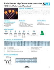
Radial Leaded High Temperature Automotive<br />
150ºC Rated Radial Leaded TransGuard ®<br />
GENERAL DESCRIPTION<br />
<strong>AVX</strong> High Temperature Multi-Layer Varistors are designed for underhood<br />
applications. <strong>Products</strong> have been tested, qualified, and specified to 150ºC. The<br />
Radial Leaded TransGuard is built for durability in harsh environments. The MLV<br />
advantage is EMI/RFI attenuation in the off state. This allows designers to combine<br />
the circuit protection and EMI/RFI attenuation function into a single highly reliable<br />
device.<br />
GENERAL<br />
CHARACTERISTICS<br />
• Operating Temperatures:<br />
-55ºC to +150ºC<br />
• Working Voltage:<br />
14-48Vdc<br />
FEATURES<br />
• Rated at 150ºC<br />
• AEC Q200 qualified<br />
• ESD rated to 25kV (HBM ESD Level 6)<br />
• EMI/RFI attenuation in off state<br />
• Excellent current and energy handling<br />
APPLICATIONS<br />
• Under hood<br />
• Down Hole Drilling<br />
• Any high temperature application<br />
HOW TO ORDER<br />
VR15<br />
AT<br />
18<br />
A<br />
650<br />
R<br />
TR2<br />
<strong>AVX</strong> Style<br />
VR15<br />
VR20<br />
Series<br />
AT = 150ºC<br />
Automotive<br />
Voltage<br />
14 = 14V<br />
18 = 18V<br />
26 = 26V<br />
48 = 48V<br />
Energy<br />
A = 0.1J<br />
D = 0.4J<br />
S = 2.0J<br />
Clamping<br />
Voltage<br />
580 = 60V<br />
650 = 67V<br />
101 = 100V<br />
151 = 150V<br />
Leads<br />
R = RoHS<br />
Compliant<br />
Packaging<br />
Blank = Bulk<br />
TR1 = T&R Standard 1<br />
TR2 = T&R Standard 2<br />
ELECTRICAL CHARACTERISTICS<br />
<strong>AVX</strong> Part Number V W DC V W AC V B V C I VC I L ET ELD IP Cap Freq VJUMP P DISS<br />
VR15AT14A580 14.0 10.0 34.5±10% 60 1 10 0.1 0.15 30 120 K 27.5 0.002<br />
VR15AT18A650 18.0 13.0 41.0±10% 67 1 10 0.1 0.15 30 90 M 29 0.002<br />
VR20AT26D101 26.0 18.0 62.0±10% 100 1 10 0.4 1.5 100 225 K 48 0.008<br />
VR20AT48S151 48.0 34.0 100.0±10% 150 1 10 2.0 3.5 250 275 K 48 0.040<br />
V W (DC) DC Working Voltage [V]<br />
V W (AC) AC Working Voltage [V]<br />
V B Typical Breakdown Votage [V @ 1mA DC ]<br />
V C Clamping Voltage [V @ I IV ]<br />
I VC Test Current for V C<br />
Maximum leakage current at the working voltage [μA]<br />
I L<br />
E t<br />
E LD<br />
I P<br />
Cap<br />
V Jump<br />
P DISS<br />
<strong>Transient</strong> Energy Rating [J, 10x1000μS]<br />
Load Dump Energy (x10) [J]<br />
Peak Current Rating [A, 8x20μS]<br />
Typical capacitance [pF] @ frequency specified and 0.5V RMS<br />
Jump Start (V)<br />
Power Dissipation (W)<br />
PHYSICAL DIMENSIONS<br />
.060 (1.52)<br />
Max.<br />
W<br />
H<br />
1.0 (25.4)<br />
Min.<br />
mm (inches)<br />
<strong>AVX</strong> Style Width Height Thickness Lead Lead<br />
(W (H) (T) Spacing Diameter<br />
VR15<br />
4.32 Max. 3.81 Max. 2.54 Max. 2.54 0.508<br />
(0.170) (0.150) (0.100) (0.100) (0.020)<br />
VR20<br />
5.59 Max<br />
(0.220)<br />
5.08 Max<br />
(0.200)<br />
3.175 Max<br />
(0.125)<br />
2.54<br />
(0.100)<br />
0.508)<br />
(0.020<br />
.100 (2.54)±.030<br />
25
Radial Leaded High Temperature Automotive<br />
150ºC Rated Radial Leaded TransGuard ®<br />
Voltage (V)<br />
180<br />
160<br />
140<br />
120<br />
100<br />
80<br />
TYPICAL PERFORMANCE CURVES<br />
Typical Voltage Current Characteristics<br />
Typical Voltage Current Characteristics<br />
VR20AT48S151<br />
VR20AT26D101<br />
VR15AT18A650<br />
VR15AT14A580<br />
60<br />
40<br />
20<br />
0<br />
1.E-09 1.E-06 1.E-03 1.E+00 1.E+03<br />
Current (A)<br />
% Vb Change<br />
AEC-Q200-002 ESD Characteristics<br />
10%<br />
5%<br />
0%<br />
-5%<br />
VOLTAGE (V)<br />
ESD Wave Absorption Characteristics<br />
2500<br />
No <strong>Suppression</strong> 8kV 150 pF 330 Ohm<br />
VR20AT48S151<br />
2000<br />
VR20AT26D101<br />
VR15AT18A650<br />
1500<br />
VR15AT14A580<br />
1000<br />
-10%<br />
6 12 16 25<br />
kV Pulse<br />
500<br />
0<br />
0 20 40 60 80 100 120 140<br />
TIME (nsec)<br />
8 kV ESD Vc<br />
(150pF/330ohm IEC Network)<br />
TAPE & REEL PACKAGING OPTIONS<br />
TR1<br />
Tape & Reel Standard 1<br />
TR2<br />
Tape & Reel Standard 2<br />
0.630 (16.0)<br />
Min.<br />
0.478 (19.0)<br />
Min.<br />
26
Controlled Capacitance<br />
Multilayer Varistor<br />
GENERAL DESCRIPTION<br />
The Controlled Capacitance TransGuard is an application specific bidirectional<br />
transient voltage suppressor developed for use in mixed signal<br />
environments. The Controlled Cap MLV has three purposes: 1) reduce<br />
emissions from a high speed ASIC, 2) prevent induced E fields from<br />
conducting into the IC, and 3) clamp transient voltages<br />
By controlling capacitance of the MLV, the center frequency and 20db<br />
range for filtering purposes can be targeted. A Controlled Cap MLV can<br />
greatly improve overall system EMC performance and reduce system<br />
size.<br />
Operating Temperature: -55ºC to +125ºC<br />
HOW TO ORDER<br />
VCAC<br />
0603<br />
22<br />
A<br />
470<br />
N<br />
R<br />
P<br />
Varistor Chip<br />
Automotive<br />
Capacitance<br />
Chip Size<br />
0603<br />
Working<br />
Voltage<br />
22 = 22V<br />
26 = 26V<br />
Energy<br />
Rating<br />
A = 0.1J<br />
C = 0.3J<br />
Capacitance<br />
470 = 47pF<br />
820 = 82pF<br />
Tolerance<br />
N = ±30%<br />
M = ±20%<br />
Packaging<br />
R = 4k pcs<br />
Termination<br />
P = Ni Barrier/<br />
100% Sn (matte)<br />
<strong>AVX</strong> Part Number VW (DC) VW (AC) VB VC IL ET IP Cap<br />
Cap Case<br />
Tolerance Size<br />
VCAC060322A470NRP 22 17 32.5±25% 50 10 0.1 30 47 30% 0603<br />
VCAC060326C820MRP 26 20 36.0±15% 67 10 0.3 30 82 20% 0603<br />
V W (DC) DC Working Voltage [V] I L Maximum leakage current at the working voltage [µA]<br />
V W (AC) AC Working Voltage [V] E T <strong>Transient</strong> Energy Rating [J, 10x1000µS]<br />
V B Breakdown Votage [V @ 1mA DC ] I P Peak Current Rating [A, 8x20µS]<br />
V C Clamping Votage [V @ 1A] Cap Capacitance [pF] @ 1KHz specified and 0.5V RMS<br />
T<br />
W<br />
0603 Discrete Dimensions mm (inches)<br />
L W T BW BL<br />
BL<br />
L<br />
1.60±0.15 0.80±0.15 0.90 MAX<br />
0.35±0.15<br />
N/A<br />
(0.063±0.006) (0.031±0.006) (0.035 MAX) (0.014±0.006)<br />
27
Controlled Capacitance<br />
Multilayer Varistor<br />
80<br />
70<br />
60<br />
50<br />
V-I Curve<br />
Volt (V)<br />
40<br />
30<br />
20<br />
10<br />
0<br />
1.E-09 1.E-07 1.E-05 1.E-03 1.E-01 1.E+01 1.E+03<br />
Current (A)<br />
VCAC060322A470N<br />
VCAC060326C820M<br />
S21<br />
0<br />
-5<br />
-10<br />
Insertion Loss (dB)<br />
-15<br />
-20<br />
-25<br />
-30<br />
-35<br />
-40<br />
0.1 1 10 100 1000 10000<br />
Frequency (MHz)<br />
VCAC060322A470N<br />
VCAC060326C820M<br />
28
Miniature 0201 MLV<br />
<strong>AVX</strong> Multilayer Ceramic <strong>Transient</strong> Voltage Suppressors<br />
ESD Protection for any Circuit with Board Space Constraints<br />
GENERAL DESCRIPTION<br />
<strong>AVX</strong> 0201 Multi-Layer Varistors are designed for circuits where board space is a<br />
premium. 0201 MLV offer bi-directional ESD protection in the smallest package<br />
available today. The added advantage is EMI/RFI attenuation. 0201 MLV can replace 2<br />
diodes and the EMC capacitor for a one chip solution.<br />
The miniature size and one chip solution team to offer designers the best in ESD<br />
protection and EMI filtering in one ultra compact device.<br />
APPLICATIONS<br />
• Cell phone<br />
• PDA<br />
• Camera modules<br />
• Embedded components<br />
• Hearing aid<br />
• Any circuit with space constraints<br />
FEATURES<br />
• Capacitance 15pF to 150pF<br />
• Low V B Version<br />
• Bi-Directional protection<br />
• Fastest response time to ESD strikes<br />
• Multi-strike capability<br />
• Ultra compact 0201 case size<br />
MultiLayer Varistors (MLVs)<br />
XCVR<br />
BUS<br />
XCVR<br />
TVS Diodes<br />
BUS<br />
EMC<br />
CAP<br />
HOW TO ORDER<br />
VC<br />
0201<br />
03<br />
MLV PROTECTION METHOD<br />
SINGLE COMPONENT SOLUTION<br />
TVS & EMI<br />
V<br />
151<br />
DIODE PROTECTION METHOD<br />
THREE COMPONENT SOLUTION<br />
TVS + EMI<br />
W<br />
P<br />
Varistor<br />
Chip<br />
Chip Size<br />
0201<br />
Working<br />
Voltage<br />
03 = 3.5V<br />
Energy<br />
Rating<br />
V = 0.02J<br />
Capacitance<br />
151 = 150pF<br />
Packaging<br />
W = 7"<br />
10kpcs<br />
Termination<br />
P = Ni Barrier/<br />
100% Sn (matte)<br />
<strong>AVX</strong> Part Number V W (DC) V W (AC) V B V C I VC I L E T I P Cap<br />
VC020103V101WP 3.5 2.0<br />
4.76 min<br />
8.84 max<br />
14max 1 50 0.02 10 100pF ±30%<br />
VC020103V121WP 3.5 2.0<br />
4.76 min<br />
8.84 max<br />
14max 1 50 0.02 10 125pF ±30%<br />
VC020103V151WP 3.5 2.0<br />
4.76 min<br />
8.84 max<br />
14max 1 50 0.02 10 150pF ±30%<br />
VC020105T150WP 5.6 4.0<br />
10.0 min<br />
15.6 max<br />
35max 1 50 0.01 2 15pF ±30%<br />
VC020105T330WP 5.6 4.0<br />
10.0 min<br />
15.6 max<br />
35max 1 50 0.01 4 33pF ±30%<br />
VC020105T500WP 5.6 4.0<br />
10.0 min<br />
15.6 max<br />
35max 1 50 0.01 5 50pF ±30%<br />
VC020105T101WP 5.6 4.0<br />
10.0 min<br />
15.6 max<br />
35max 1 50 0.01 5 100pF ±30%<br />
VC020105V101WP 5.6 4.0<br />
6.4 min<br />
9.6 max<br />
17max 1 50 0.02 4 100pF ±30%<br />
VC020107V101WP 7.0 5.6<br />
9.6 min<br />
14.4 max<br />
20max 1 50 0.02 5 100pF ±30%<br />
VC020116T150WP 16 11<br />
21.7 min<br />
29.3 max<br />
45max 1 50 0.01 1 15pF ±30%<br />
V W (DC) DC Working Voltage [V] I L Maximum leakage current at the working voltage [µA]<br />
V W (AC) AC Working Voltage [V] E T <strong>Transient</strong> Energy Rating [J, 10x1000µS]<br />
V B Breakdown Votage [V @ 1mADC] I P Peak Current Rating [A, 8x20µS]<br />
V C Clamping Votage [V @ IVC] Cap Capacitance [pF] @ 1KHz specified and 0.5VRMS<br />
I VC Test Current for VC [A, 8x20µS]<br />
29
Miniature 0201 MLV<br />
<strong>AVX</strong> Multilayer Ceramic <strong>Transient</strong> Voltage Suppressors<br />
ESD Protection for any Circuit with Board Space Constraints<br />
PHYSICAL DIMENSIONS: mm (inches)<br />
T<br />
t<br />
t<br />
Size (EIA) Lenght (L) Width (W) Max Thickness (T) Terminal (t)<br />
W<br />
0201<br />
0.60±0.03 0.30±0.03 0.33 max. 0.15±0.05<br />
(0.024±.001) (0.011±0.001) (0.013 max.) (0.006±0.002)<br />
L<br />
VOLTAGE/CURRENT CHARACTERISTICS<br />
50.0<br />
TRANSMISSION CHARACTERISTICS<br />
5.6Vdc<br />
0<br />
Votage (V)<br />
37.5<br />
25.0<br />
12.5<br />
0<br />
Insertion Loss (dB)<br />
-5<br />
-10<br />
-15<br />
-20<br />
-25<br />
-30<br />
-35<br />
-40<br />
1E-09 1E-08 1E-07 1E-06 1E-05 1E-04 1E-03 1E-02 1E-01 1E+00 1E+01<br />
-45<br />
Current (A)<br />
-50<br />
0.1 1 10 100 1000 10000<br />
16 V 3.5 V 5.6 V 7 V<br />
Frequency (MHz)<br />
TYPLICAL 8 KV ESD PERFORMANCE<br />
(150pF / 300ohm IEC Network)<br />
15 pF 33 pF 50 pF 100 pF<br />
3.5Vdc<br />
0<br />
30<br />
-5<br />
Vb<br />
25<br />
20<br />
15<br />
10<br />
5<br />
Insertion Loss (dB)<br />
-10<br />
-15<br />
-20<br />
-25<br />
-30<br />
-35<br />
-40<br />
-45<br />
0<br />
0 1 10 100 1000<br />
-50<br />
0.1 1.0 10.0 100.0 1000.0 10000.0<br />
# Pulses<br />
Frequency (MHz)<br />
15 pF 33 pF 50 pF 100 pF<br />
125 pF 150 pF<br />
8kV CONTACT ESD vs PULSE 1 Mohm Input<br />
(150pF / 330ohm Network)<br />
Voltage (V)<br />
2500<br />
1875<br />
1250<br />
625<br />
0<br />
0 25 50 75 100<br />
Time (n sec)<br />
16 V 3.5 V 5.6 V 7 V<br />
Insertion Loss (dB)<br />
0<br />
-5<br />
-10<br />
-15<br />
-20<br />
-25<br />
-30<br />
-35<br />
-40<br />
-45<br />
-50<br />
0.1 1.0 10.0 100.0 1000.0 10000.0<br />
Frequency (MHz)<br />
30
High Temperature Automotive<br />
150ºC Rated Varistors<br />
GENERAL DESCRIPTION<br />
<strong>AVX</strong> High Temperature Multi-Layer Varistors are designed for underhood applications.<br />
<strong>Products</strong> have been tested, qualified, and specified to 150ºC. The MLV<br />
advantage is EMI/RFI attenuation in the off state. This allows designers the ability<br />
to combine the circuit protection and EMI/RFI attenuation function into a single<br />
highly reliable device.<br />
FEATURES<br />
• Rated at 150°C<br />
• AEC Q200 qualified<br />
• ESD rating to 25kV contact<br />
• EMI/RFI attenuation in off state<br />
• Excellent current and energy handling<br />
APPLICATIONS<br />
• Under hood<br />
• Down Hole Drilling<br />
• Any high temperature application<br />
CAN SERIES<br />
HOW TO ORDER<br />
CAN<br />
AT<br />
01<br />
R<br />
P<br />
Type<br />
Controlled Area<br />
Network Varistor<br />
Series<br />
Automotive<br />
High Temperature<br />
Case Size<br />
01 = 0603<br />
02 = 0405 2-Element<br />
04 = 0612 4-Element<br />
Packaging<br />
D = 7” (1000 pcs)<br />
R = 7” (4,000 pcs)<br />
T = 13” (10,000pcs)<br />
Termination<br />
P = Ni Barrier/<br />
100% Sn (matte)<br />
<strong>AVX</strong> Part Number V W (DC) V W (AC) V B I L E T I P Cap Case Size Elements<br />
CANAT01-- ≤ 18 ≤ 14 120 10 0.015 4 22 0603 1<br />
CANAT02-- ≤ 18 ≤ 14 70 10 0.015 4 22 0405 2<br />
CANAT04-- ≤ 18 ≤ 14 100 10 0.015 4 22 0612 4<br />
V W (DC) DC Working Voltage [V] I L Maximum leakage current at the working voltage [µA]<br />
V W (AC) AC Working Voltage [V] E T <strong>Transient</strong> Energy Rating [J, 10x1000µS]<br />
V B Breakdown Votage [V @ 1mA DC ] I P Peak Current Rating [A, 8x20µS]<br />
V C Clamping Votage [V @ IVC] Cap Capacitance [pF] @ 1KHz specified and 0.5VRMS<br />
ANTENNAGUARD SERIES<br />
HOW TO ORDER<br />
VCAT<br />
06<br />
AG<br />
18<br />
120<br />
Y<br />
A<br />
T<br />
1<br />
A<br />
Type<br />
High Temperature<br />
Varistor<br />
Case Size<br />
04 = 0402<br />
06 = 0603<br />
Varistor Series<br />
AntennaGuard<br />
Working<br />
Voltage<br />
18 = 18Vdc<br />
Cap<br />
Non-Std.<br />
Cap Tolerance<br />
N/A<br />
Termination<br />
Finish<br />
P = Ni Barrier/<br />
100% Sn<br />
Reel<br />
Size<br />
1 = 7"<br />
3 = 13"<br />
Reel<br />
Quantity<br />
A = 4000 or<br />
10,000<br />
<strong>AVX</strong> Part Number V W (DC) V W (AC) I L Cap Cap Tolerance Case Size<br />
VCAT06AG18120YAT-- ≤ 18 ≤ 14 10 12 +4, -2pF 0603<br />
V W (DC) DC Working Voltage [V] I L Maximum leakage current at the working voltage [µA]<br />
V W (AC) AC Working Voltage [V] Cap Capacitance [pF] @ 1KHz specified and 0.5VRMS<br />
31
High Temperature Automotive<br />
150ºC Rated Varistors<br />
PHYSICAL DIMENSIONS<br />
T<br />
W<br />
P<br />
W<br />
P<br />
W<br />
T<br />
T<br />
BL<br />
L<br />
BW<br />
BW<br />
BL<br />
L<br />
BL<br />
L<br />
0603 Discrete Dimensions mm (inches)<br />
L W T BW BL P<br />
1.60±0.15 0.80±0.15 0.90 MAX<br />
0.35±0.15<br />
N/A<br />
(0.063±0.006) (0.032±0.006) (0.035 MAX) (0.014±0.006)<br />
0405 2 Elements Array Dimensions mm (inches)<br />
L W T BW BL P<br />
1.00±0.15 1.37±0.15 0.66 MAX 0.36±0.10 0.20±0.10 0.64 REF<br />
(0.039±0.006) (0.054±0.006) (0.026 MAX) (0.014±0.004) (0.008±0.004) (0.025 REF)<br />
0612 4 Elements Array Dimensions mm (inches)<br />
L W T BW BL P<br />
1.60±0.20 3.20±0.20 1.22 MAX 0.41±0.10 0.18 0.76 REF<br />
+0.25<br />
-0.08<br />
(0.063±0.008) (0.126±0.008) (0.048 MAX) (0.016±0.004)<br />
+.010<br />
(0.008 -.003) (0.030 REF)<br />
N/A<br />
32
Glass Encapsulated SMD Varistor MLV<br />
(VJ12, 20, 13, 14, 15, 32)<br />
<strong>Transient</strong> Voltage <strong>Suppression</strong>, ESD Protection Devices & EMI Devices<br />
GENERAL DESCRIPTION<br />
<strong>AVX</strong>’s Professional Multilayer Varistors include 3 series of<br />
glass coated products as listed below:<br />
• Standard M0 Series<br />
• Telecom MT Series<br />
• Automotive MA/PA Series<br />
The glass encapsulation process ensures high insulation<br />
resistance values after reflow soldering and excellent SMT<br />
compatibility. This protection ensures reliability and acidresistance<br />
against harsh environment like chlorite flux.<br />
TYPICAL APPLICATIONS<br />
Mainly used to reduce transient over-voltages in a very wide<br />
range of electronic products. Some example applications<br />
are:<br />
1) Telecom, 2) Automotive, 3) Consumer Electronics, and<br />
4) Industrial Applications.<br />
PHYSICAL CHARACTERISTICS<br />
Construction Weight:
Glass Encapsulated SMD Varistor MLV<br />
(VJ12, 20, 13, 14, 15, 32)<br />
Automotive MLV Range – MA and PA Series<br />
AUTOMOTIVE SERIES – VJ12, 20, 13, 14, 15, 32 MA and PA SERIES<br />
FEATURES<br />
• Available in case size 0805, 1206, 1210, 1812, 2220,<br />
(3220 under development)<br />
• Nickel and Tin (100%) plated Termination<br />
• Max Energy absorption: 1.5 to 25J (50J under<br />
development)<br />
• Well suited to protect against automotive related transients<br />
• Load Dump capabilities: according to ISO standard<br />
DP7637-2 12V and 24V pulse 5<br />
• Jump start capability (12V): 24.5 V - 5mn<br />
• Complying to main requirements of AECQ 200<br />
• RoHS Compliant and IMDS Registration<br />
PART NUMBERS<br />
GENERAL CHARACTERISTICS<br />
Storage Temperature: -55ºC to +150ºC<br />
Operating Temperature: -55ºC to +125ºC*<br />
* 150°C upon request<br />
APPLICATIONS<br />
• Protection of various semiconductor elements from<br />
overvoltage.<br />
• Absorption of switching surge and electrostatic surge for<br />
relays and motors.<br />
• Protection of electronic equipment for automobiles from<br />
induced lightning surge.<br />
Part Number Case Size Working Breakdown Peak Maximum Energy Energy Jump Start T max<br />
EIA Voltage Voltage current leakage 10*1000µs Load-Dump<br />
current at Vdc<br />
(x10)<br />
Vdc V(1mA) Amp. 8*20µs µA Joules Joules Vmax Thickness<br />
(5mn min.) mm (inches)<br />
*VJ12PA0160--- 0805 16 24.5 120 20 0.3 1 24.5 1.3<br />
VJ20MA0160--- 1206 16 24.5 200 20 0.6 1.5 24.5 1.7<br />
VJ20PA0160--- 1206 16 24.5 300 20 1.1 2 24.5 1.7<br />
VJ13MA0160--- 1210 16 24.5 400 20 1.6 3 24.5 1.7<br />
VJ13PA0160--- 1210 16 24.5 500 20 2 5 24.5 1.7<br />
VJ14MA0160--- 1812 16 24.5 800 20 2.4 6 25.5 2<br />
VJ14PA0160--- 1812 16 24.5 1000 20 2.9 10 25.5 2<br />
VJ15MA0160--- 2220 16 24.5 1200 20 5.8 12 25.5 2<br />
VJ15PA0160--- 2220 16 24.5 1500 20 7.2 25 25.5 2<br />
VJ32PA0160--- 3220 16 24.5 2000 20 13.8 50 24.5 2.5<br />
VJ15MA0340--- 2220 34 47 1200 20 10 12 47 2.5<br />
VJ15PA0340--- 2220 34 47 2000 20 13 25 47 2.5<br />
*VJ32PA0340 3220 34 47 2000 20 19 50 47 2.5<br />
* under development<br />
Hybrid termination AgPdPt upon request<br />
TEMPERATURE CHARACTERISTICS<br />
For Current, Energy and Power<br />
Percent of Rating Value<br />
120<br />
100<br />
80<br />
60<br />
40<br />
20<br />
0<br />
-55 -25 0 25 50 75 100 125 150<br />
Ambient Temperature (°C)<br />
IMPEDANCE CHARACTERISTICS<br />
Z (Ohms)<br />
100<br />
10<br />
1<br />
0.1<br />
VJ15PA0160K<br />
VJ15MA0160K<br />
VJ14MA0160K<br />
VJ13MA0160K<br />
VJ20MA0160K<br />
VJ15MA0340K<br />
0.01<br />
1,000 10,000 100,000<br />
Frequency (kHz)<br />
1,000,000<br />
34
Glass Encapsulated SMD Varistor MLV<br />
(VJ12, 20, 13, 14, 15, 32)<br />
Automotive MLV Range – MA and PA Series<br />
AUTOMOTIVE SERIES – VJ12, 20, 13, 14, 15, 32 MA and PA SERIES<br />
V / I CHARACTERISTICS<br />
PULSE RATING<br />
V (V)<br />
200<br />
150<br />
100<br />
50<br />
V / I Characteristics : Automotive Parts<br />
VJ20MA0160K<br />
VJ13MA0160K<br />
VJ14MA0160K<br />
VJ14PA0160K<br />
VJ15MA0160K<br />
VJ15PA0160K<br />
VJ15PA0340K<br />
VJ32PA0160K<br />
0<br />
1E-06 0.00001 0.0001 0.001 0.01 0.1 1 10 100 1000 10000<br />
I (A)<br />
% of peak current rating<br />
100.00%<br />
10.00%<br />
1.00%<br />
T<br />
Pulse Rating<br />
A% max<br />
1 Repetition (Top)<br />
2 Repetitions<br />
10 Repetitions<br />
10E2 Repetitions<br />
10E3 Repetitions<br />
10E4 Repetitions<br />
10E5 Repetitions<br />
10E6 Repetitions<br />
Infinite (bottom)<br />
0.10%<br />
10 100 1000 10000<br />
Pulse Duration (µs)<br />
TEMPERATURE DEPENDENCE OF V/I CHARACTERISTICS<br />
V/V1mA (%)<br />
100<br />
VJ20MA0160K<br />
V/V1mA (%)<br />
100<br />
VJ13MA0160K<br />
-40°C<br />
+25°C<br />
+85°C<br />
+125°C<br />
-40°C<br />
+25°C<br />
+85°C<br />
+125°C<br />
10<br />
1E-07 1E-06 1E-05 1E-04 1E-03 1E-02<br />
Current (A)<br />
10<br />
1E-06 1E-05 1E-04 1E-03 1E-02<br />
Current (A)<br />
V/V1mA (%)<br />
100<br />
VJ14MA0160K<br />
-40°C<br />
+25°C<br />
V/V1mA (%)<br />
100<br />
VJ15MA0160K<br />
-40°C<br />
+25°C<br />
+85°C<br />
+125°C<br />
+85°C<br />
+125°C<br />
10<br />
1E-07 1E-06 1E-05 1E-04 1E-03 1E-02<br />
Current (A)<br />
10<br />
1E-07 1E-06 1E-05 1E-04 1E-03 1E-02 1E-01<br />
Current (A)<br />
35
Glass Encapsulated SMD Varistor MLV<br />
(VJ12, 20, 13, 14, 15, 32)<br />
Automotive MLV Range – MA and PA Series<br />
Voltage as a percent of<br />
breakdown voltage<br />
1,000<br />
100<br />
AUTOMOTIVE SERIES – VJ12, 20, 13, 14, 15, 32 MA and PA SERIES<br />
VJ14PA0160<br />
+25°C<br />
+25°Cinter (%)<br />
+25°Cfinal (%)<br />
+85°C<br />
+125°C<br />
10<br />
1E-07 1E-06 1E-05 1E-04 1E-03 1E-02 1E-01<br />
Current (A)<br />
100<br />
VJ15MA0340K<br />
V/V1mA (%)<br />
100<br />
VJ15PA0160K<br />
-40°C<br />
+25°C<br />
+85°C<br />
+125°C<br />
10<br />
1E-07 1E-06 1E-05 1E-04 1E-03 1E-02<br />
C<br />
t (A)<br />
-40°C<br />
+25°C<br />
+85°C<br />
+125°C<br />
10<br />
1E-07 1E-06 1E-05 1E-04 1E-03 1E-02<br />
Current (A)<br />
Change in breakdown<br />
voltage (%)<br />
PULSE DEGRADATION<br />
Repetitive Peak Current Strikes<br />
16%<br />
14%<br />
VJ20MA0160K @200A<br />
12%<br />
VJ13MA0160K @400A<br />
10%<br />
VJ14MA0160K @800A<br />
8%<br />
VJ14PA0160K @1000A<br />
VJ15PA0160K @1200A<br />
6%<br />
VJ15MA0160K @1200A<br />
4%<br />
VJ15MA0340K @1200A<br />
2%<br />
0%<br />
0 100 200 300 400 500 600<br />
Number of strikes<br />
36
Glass Encapsulated SMD Varistor MLV<br />
(VJ12, 20, 13, 14, 15, 32)<br />
Automotive MLV Range – MA and PA Series<br />
AUTOMOTIVE SERIES – VJ12, 20, 13, 14, 15, 32 MA and PA SERIES<br />
AUTOMOTIVE LOAD DUMP TEST<br />
(According to ISO DP7637/2 Pulse 5)<br />
V z<br />
90%<br />
10%<br />
When using the test method indicated below,<br />
the amount of Energy dissipated by the<br />
varistor must not exceed the Load Dump<br />
Energy value specified in the product table.<br />
V i<br />
0V<br />
Tr<br />
Td<br />
t<br />
Voltage Pulse applied to the varistor:<br />
12V Network<br />
Vi = 13.5V<br />
Td = 100 to 350ms<br />
Ri = 2 Ohms (Internal Resistance)<br />
Vz - 70 to 200V<br />
Number of Pulses = 10 Pulses<br />
Other Load Dump Simulations can be achieved<br />
24V Network<br />
Vi = 27V<br />
Td = 100 to 350ms<br />
Ri = 2 Ohms (Internal Resistance)<br />
Vz - 70 to 200V<br />
Number of Pulses = 10 Pulses<br />
Pulse 5: Typical Vz max versus Pulse duration and Rs<br />
VJ20MA0160K 0.5 Ohm 1 Ohm 2 Ohms<br />
50ms 33 34 39<br />
100ms 31 31 34<br />
200ms 27 28 33<br />
400ms 28 30 34<br />
VJ13PA0160K 0.5 Ohm 1 Ohm 2 Ohms<br />
50ms 44 48 57<br />
100ms 36 39 46<br />
200ms 33 33 39<br />
400ms 29 28 34<br />
VJ14PA0160K 0.5 Ohm 1 Ohm 2 Ohms<br />
50ms 60 68 85<br />
100ms 46 52 62<br />
200ms 37 41 50<br />
400ms 32 35 43<br />
VJ15PA0160K 0.5 Ohm 1 Ohm 2 Ohms<br />
50ms 98 116 150<br />
100ms 66 80 104<br />
200ms 50 60 78<br />
400ms 41 47 58<br />
VJ32PA0160K 0.5 Ohm 1 Ohm 2 Ohms<br />
50ms 146 186 200<br />
100ms 105 131 179<br />
200ms 72 88 113<br />
400ms 54 67 96<br />
37
Glass Encapsulated SMD Varistor MLV<br />
(VJ12, 20, 13, 14, 15)<br />
Industrial MLV Range – M0 Series<br />
INDUSTRIAL MLV RANGE – VJ12, 20, 13, 14, 15 M0 SERIES<br />
FEATURES<br />
• Glass encapsulation device with very low leakage current<br />
under DC operating conditions<br />
• Device available in case size 1206, 1210, 1812, 2220<br />
(3220)<br />
• Nickel and Tin (100%) plated Termination (Hybrid AgPdPt<br />
termination available upon request)<br />
• Bi-Directional protection. Fast Turn-On Time.<br />
• Excellent transient clamping characteristics up to<br />
1200amps peak current<br />
• Multi strike capability. Provide EMC Capacitance<br />
• RoHS Compliant<br />
GENERAL CHARACTERISTICS<br />
Storage Temperature: -55ºC to +150ºC<br />
Operating Temperature: -55ºC to +125ºC<br />
TYPICAL APPLICATIONS<br />
Many uses to reduce transient over-voltage in the very wide<br />
range of electronic products in the Professional, Industrial<br />
and Consumer Applications.<br />
Type Case Size Vrms VDC<br />
Max.<br />
Maximum<br />
Max. Peak Cap.<br />
Breakdown<br />
Energy<br />
Clamping<br />
Leakage<br />
Current Typical<br />
Voltage<br />
10*1000µs<br />
Voltage Current 8*20µs (1KHz/0.5V)<br />
(V) (V) (V) Vp (V) lp (A) µA (J) (A) (pF)<br />
VJ20M00140K--- 1206 14 18 22±10% 38 1 20 0.5 200 900<br />
VJ13M00140K--- 1210 14 18 22±10% 38 2.5 20 1.6 400 1800<br />
VJ14M00140K--- 1812 14 18 22±10% 38 5 20 2.3 800 4200<br />
VJ15M00140K--- 2220 14 18 22±10% 38 10 20 5.8 1200 9600<br />
VJ20M00170K--- 1206 17 22 27±10% 44 1 20 0.6 200 800<br />
VJ13M00170K--- 1210 17 22 27±10% 44 2.5 20 1.7 500 2500<br />
VJ14M00170K--- 1812 17 22 27±10% 44 5 20 2.7 800 3700<br />
VJ15M00170K--- 2220 17 22 27±10% 44 10 20 7.2 1200 8600<br />
VJ20M00200K--- 1206 20 26 33±10% 54 1 20 0.7 200 550<br />
VJ13M00200K--- 1210 20 26 33±10% 54 2.5 20 1.9 500 1200<br />
VJ14M00200K--- 1812 20 26 33±10% 54 5 20 3 800 2800<br />
VJ15M00200K--- 2220 20 26 33±10% 54 10 20 7.8 1200 6400<br />
VJ20M00250K--- 1206 25 31 39±10% 65 1 20 1 200 500<br />
VJ13M00250K--- 1210 25 31 39±10% 65 2.5 20 1.7 500 1100<br />
VJ14M00250K--- 1812 25 31 39±10% 65 5 20 3.7 800 2600<br />
VJ15M00250K--- 2220 25 31 39±10% 65 10 20 9.6 1200 5800<br />
VJ20M00300K--- 1206 30 38 47±10% 77 1 20 1.1 200 400<br />
VJ13M00300K--- 1210 30 38 47±10% 77 2.5 20 2 400 1200<br />
VJ14M00300K--- 1812 30 38 47±10% 77 5 20 4.2 800 1800<br />
VJ15M00300K--- 2220 30 38 47±10% 77 10 20 12 1200 4200<br />
VJ20M00350K--- 1206 35 45 56±10% 90 1 20 0.6 200 260<br />
VJ13M00350K--- 1210 35 45 56±10% 90 2.5 20 1.5 300 1200<br />
VJ14M00350K--- 1812 35 45 56±10% 90 5 20 4 500 2500<br />
VJ15M00350K--- 2220 35 45 56±10% 90 10 20 10 1000 4000<br />
VJ20M00400K--- 1206 40 56 68±10% 110 1 20 0.7 100 190<br />
VJ13M00400K--- 1210 40 56 68±10% 110 2.5 20 2.3 250 380<br />
VJ14M00400K--- 1812 40 56 68±10% 110 5 20 4.8 500 800<br />
VJ15M00400K--- 2220 40 56 68±10% 110 10 20 9 1000 2000<br />
VJ20M00500K--- 1206 50 65 82±10% 135 1 20 0.8 100 130<br />
VJ13M00500K--- 1210 50 65 82±10% 135 2.5 20 1.6 250 700<br />
VJ14M00500K--- 1812 50 65 82±10% 135 5 20 4.5 400 600<br />
VJ15M00500K--- 2220 50 65 82±10% 135 10 20 7 800 1400<br />
VJ20M00600K--- 1206 60 85 100±10% 165 1 20 0.9 100 100<br />
VJ13M00600K--- 1210 60 85 100±10% 165 2.5 20 1.5 250 600<br />
VJ14M00600K--- 1812 60 85 100±10% 165 5 20 4.5 400 500<br />
VJ15M00600K--- 2220 60 85 100±10% 165 10 20 6.8 800 1100<br />
38
Glass Encapsulated SMD Varistor MLV<br />
(VJ12, 20, 13, 14, 15)<br />
Industrial MLV Range – M0 Series<br />
INDUSTRIAL MLV RANGE – VJ12, 20, 13, 14, 15 M0 SERIES<br />
V/I CHARACTERISTIC<br />
150<br />
VI Curves 18V, 22V, and 26V<br />
Voltage (V)<br />
100<br />
50<br />
18V, 1.6J<br />
22V, 1.6J<br />
26V, 1.9J<br />
26V, 3J<br />
0<br />
1E-06 0.00001 0.0001 0.001 0.01 0.1 1 10 100 1000<br />
Current (A)<br />
Voltage (V)<br />
200<br />
150<br />
100<br />
VI Curves 31V, 38V, and 45V<br />
31V, 1.7J<br />
38V, 1.1J<br />
38V, 2J<br />
38V, 4.2J<br />
45V, 1.5J<br />
50<br />
0<br />
1E-06<br />
0.00001 0.0001 0.001 0.01 0.1 1 10 100 1000<br />
Current (A)<br />
250<br />
VI Curves 56V, 65V, and 85V<br />
Voltage (V)<br />
200<br />
150<br />
100<br />
56V<br />
65V, 1.6J<br />
85V, 1.5J<br />
50<br />
0<br />
1E-06 0.00001 0.0001 0.001 0.01 0.1 1 10 100 1000<br />
Current (A)<br />
39
Glass Encapsulated SMD Varistor MLV<br />
(VJ14)<br />
Telecom MLV Range – MT Series<br />
FEATURES<br />
• Effective alternative to leaded MOVs between 60 and<br />
90 Vrsm<br />
• High Energy Ratings up to 6 Joules with 1812 case size<br />
• Nickel barrier or hybrid AgPdPt terminations<br />
• Multiple Strike Capability<br />
• Provide EMC Capacitance<br />
• Specified in accordance to CCITT 10/1000μs Pulse test<br />
• RoHS Compliant and IMDS Registration<br />
TELECOM MLV RANGE - VJ14 MT SERIES<br />
TARGET APPLICATIONS<br />
• Phone Lines, ADSL Lines, and other Telecom Circuits<br />
• Consumer <strong>Products</strong><br />
GENERAL CHARACTERISTICS<br />
Storage Temperature: -55ºC to +125ºC<br />
Operating Temperature: -55ºC to +125ºC<br />
CCITT 10x700µs TEST<br />
A pulse of 10 x 700μs duration as specified by CCITT or IEC<br />
61000-4-5 is often used to check the interference immunity<br />
of Telecom equipment.<br />
The curves show that the 60Vrms Varistor can reduce the<br />
interference of the equipment from 2KV to less than 200V.<br />
Voltage<br />
2000<br />
1500<br />
1000<br />
10/700 Telecom Test Pulse Wave-Form<br />
Without Varistor<br />
(Open-circuit voltage)<br />
dV/V1mA<br />
10%<br />
8%<br />
6%<br />
4%<br />
2%<br />
10/700 Pulse Test Capability<br />
Typical V1mA Drift<br />
60Vrms<br />
95Vrms<br />
500<br />
With a 60Vrms Telecom Varistor<br />
(Protection level
Glass Encapsulated SMD Varistor MLV<br />
(VJ32/VC32)<br />
GENERAL DESCRIPTION<br />
The VJ32/VC32M0 Series offers the designer a<br />
surface mount solution with higher voltage<br />
ratings and transient energy ratings. This<br />
Multilayer Layer Surface Mount Varistor replaces<br />
the traditional radial-lead Varistors with reduced<br />
size and weight. The glass encapsulation ensures<br />
the high performances in voltage up to 300Vrms<br />
reliability and acid-resistance against harsh<br />
environment like chlorite soldering flux.<br />
LEAD-FREE COMPATIBLE<br />
COMPONENT<br />
FEATURES<br />
• Lead less surface mount chip 3220 Case Size<br />
• Voltage Ratings from 175Vrms to 300 Vrms<br />
• VJ32 with Ni barrier/100% Sn Termination (for lead free<br />
soldering applications)<br />
VC32 with hybrid PdPtAg Termination (not suitable for<br />
lead free soldering)<br />
• Operating temperature from -55°C to +85°C<br />
• RoHS Compliant<br />
APPLICATIONS<br />
• MOV (Radial) Replacement<br />
• <strong>Suppression</strong> of transient on line voltage<br />
• Electric Meters<br />
• Industrial Equipment<br />
• Mains PSUs<br />
• Telecommunications<br />
• Consumer Electronics<br />
PART NUMBERS<br />
Max. Peak<br />
Max.<br />
Cap.<br />
Max. Clamping Voltage<br />
Energy Current<br />
Operating voltage Breakdown Voltage Voltage at 1mA<br />
Leakage<br />
Typical<br />
<strong>AVX</strong> PN Case Size 8*20µs<br />
10*1000µs 8*20µs<br />
Current<br />
(1KHz,0.5V)<br />
1 Pulse<br />
Vrms Vdc Min. Average Max. V A µA Joule A pF<br />
VJ32M01750K-- 3220 175 225 245 270 297 455 10 15 9.5 300 120<br />
VJ32M00231K-- 3220 230 300 327 360 396 595 10 15 10 300 80<br />
VJ32M00251K-- 3220 250 330 355 390 429 650 10 15 11 300 75<br />
VJ32M02750K-- 3220 275 369 391 430 473 710 10 15 13 300 70<br />
VJ32M00301K-- 3220 300 385 427 470 517 775 10 15 15 300 65<br />
41
Glass Encapsulated SMD Varistor MLV<br />
(VJ13, 14, 15, 20)<br />
Surface Mounting Guide<br />
SOLDERABILITY/LEACHING<br />
SURFACE MOUNTING GUIDE (VJ13, 14, 15, 20)<br />
APPLICATIONS NOTES<br />
Terminations to be well soldered after immersion in a 60/40<br />
tin/lead solder bath at 235±5ºC for 2±1 seconds.<br />
Terminations will resist leaching for at least the immersion<br />
times and conditions recommendations shown below.<br />
P/N Termination Type<br />
Solder Solder Immersion<br />
Tin/Lead Temp. ºC Time (sec)<br />
Plated MLV<br />
VJ Nickel and Matte Tin 60/40 260±5 30±1<br />
Plating Termination<br />
a) The visual standards used for evaluation of solder joints<br />
will need to be modified as lead free joints are not as<br />
bright as with tin-lead pastes and the fillet may not be as<br />
large.<br />
b) Lead-free solder pastes do not allow the same self alignment<br />
as lead containing systems. Standard mounting<br />
pads are acceptable, but machine set up may need to<br />
be modified.<br />
D2<br />
Ceramic<br />
Unplated MLV<br />
Electrodes<br />
Thick<br />
Film<br />
Material<br />
Ceramic<br />
Electrodes<br />
Plated MLV<br />
Solder Layer<br />
Nickel Layer<br />
Thick<br />
Film<br />
Material<br />
RECOMMENDED SOLDERING PROFILES<br />
VJ products are compatible with a wide range of soldering<br />
conditions consistent with good manufacturing practice for<br />
surface mount components. This includes Pb free reflow<br />
processes and peak temperatures up to 270ºC.<br />
Recommended profiles for reflow and wave soldering are<br />
show below for reference.<br />
VC products are recommended for lead soldering application<br />
or gluing techniques.<br />
Temperature (ºC)<br />
300<br />
250<br />
200<br />
150<br />
100<br />
50<br />
VJ <strong>Products</strong> Lead-Free Reflow Profile<br />
MAXIMUM TEMPERATURE 260ºC<br />
20 - 40 SECONDS WITH 5ºC<br />
RAMP RATE<br />
< 3ºC/s<br />
PREHEAT ZONE<br />
60 - 150 SEC<br />
> 217ºC<br />
RECOMMENDED<br />
SOLDER PAD<br />
LAYOUT<br />
REFLOW SOLDERING<br />
Case<br />
Size<br />
D1 D2 D3 D4 D5<br />
1206 4.00 (0.157) 1.00 (0.039) 2.00 (0.079) 1.00 (0.039) 1.06 (0.042)<br />
1210 4.00 (0.157) 1.00 (0.039) 2.00 (0.079) 1.00 (0.039) 2.05 (0.081)<br />
1812 5.60 (0.220) 1.00 (0.039) 3.60 (0.142) 1.00 (0.039) 3.00 (0.118)<br />
2220 6.60 (0.260) 1.00 (0.039) 4.60 (0.181) 1.00 (0.039) 5.00 (0.197)<br />
3220 10.21 (0.402) 2.21 (0.087) 5.79 (0.228) 2.21 (0.087) 5.50 (0.217)<br />
WAVE SOLDERING<br />
D1<br />
D3<br />
D4<br />
D5<br />
Dimensions in mm (inches)<br />
Dimensions in mm (inches)<br />
Case<br />
Size<br />
D1 D2 D3 D4 D5<br />
1206 5.00 (0.197) 1.50 (0.059) 2.00 (0.079) 1.50 (0.059) 1.06 (0.042)<br />
1210 5.00 ( 0.197) 1.50 (0.059) 2.00 (0.079) 1.50 (0.059) 2.05 (0.081)<br />
1812 6.60 (0.260) 1.50 (0.059) 3.60 (0.142) 1.50 (0.059) 3.00 (0.118)<br />
2220 7.60 (0.299) 1.50 (0.059) 4.60 (0.181) 1.50 (0.059) 5.00 (0.197)<br />
3220 11.21 (0.441) 1.50 (0.059) 5.79 (0.228) 1.50 (0.059) 5.50 (0.217)<br />
0<br />
0 1.0 2.0 3.0 4.0 5.0 6.0 7.0<br />
42
Glass Encapsulated TransGuard ®<br />
GENERAL DESCRIPTION<br />
The Glass Encapsulated TransGuard ® multilayer varistors are<br />
zinc oxide (ZnO) based ceramic semiconductor devices with<br />
non-linear, bi-directional V-I characteristics.<br />
They have the advantage of offering bi-directional<br />
overvoltage protection as well as EMI/RFI attenuation in a<br />
single SMT package.<br />
These large case size parts extend TransGuard range into<br />
high energy applications. In addition the glass encapsulation<br />
provides enhanced resistance against harsh environment or<br />
process such as acidic environment, salts or chlorite flux.<br />
GENERAL<br />
CHARACTERISTICS<br />
Operating Temperature:<br />
-55ºC to 125ºC<br />
FEATURES<br />
• Bi-Directional protection<br />
• EMI/RFI attenuation in off-state<br />
• Multi-strike capability<br />
• Sub 1nS response to ESD strike<br />
• High energy / High current<br />
• Glass Encapsulated<br />
APPLICATIONS<br />
• Proffesional / Industrial / Commercial Applications<br />
• IC Protection, DC motor protection<br />
• Relays, Controllers, Sensors<br />
• Smart Grids<br />
• Alarms and more<br />
• Various Applications where Glass Encapsulation is<br />
Needed for Harsh Environment / Acid-Resistance<br />
HOW TO ORDER<br />
V<br />
G<br />
1812<br />
16<br />
P<br />
400<br />
R<br />
P<br />
Varistor<br />
Glass<br />
Encapsulate<br />
Chip<br />
Chip Size<br />
1210<br />
1812<br />
2220<br />
Working<br />
Voltage<br />
16 = 16Vdc<br />
22 = 22Vdc<br />
38 = 38Vdc<br />
65 = 65Vdc<br />
Engergy<br />
Rating<br />
S = 2.0J<br />
P = 2.7-3.0J<br />
U = 4.0-5.0J<br />
Y = 7.2-12J<br />
Clamping<br />
Voltage<br />
400 = 42V<br />
440 = 44V<br />
770 = 77V<br />
131 = 135V<br />
Package<br />
D = 7" reel<br />
R = 7" reel<br />
T = 13" reel<br />
Termination<br />
P = Ni/Sn plated<br />
PHYSICAL DIMENSIONS: mm (inches)<br />
Size (EIA) Length (L) Width (W) Max Thickness (T) Land Length (t)<br />
1210<br />
3.20±0.20 2.49±0.20 1.70 0.14 max.<br />
(0.126±0.008) (0.098±0.008) (0.067) (0.045 max.)<br />
1812<br />
4.50±0.30 3.20±0.30 2.00 1.00 max.<br />
(0.177±0.012) (0.126±0.012) (0.079) (0.040 max.)<br />
2220<br />
5.70±0.40 5.00±0.40 2.50 1.00 max.<br />
(0.224±0.016) (0.197±0.016) (0.098) (0.040 max.)<br />
43
Glass Encapsulated TransGuard ®<br />
ELECTRIAL CHARACTERISTICS<br />
<strong>AVX</strong> PN V W (DC) V W (AC) V B V C I VC I L E T I P Cap Freq<br />
VG181216P400 16 11 24.5±10% 42 5 10 2.9 1000 5000 K<br />
VG222016Y400 16 11 24.5±10% 42 10 10 7.2 1500 13000 K<br />
VG121022R440 22 17 27±10% 44 2.5 10 1.7 400 1600 K<br />
VG121038S770 38 30 47.0±10% 77 2.5 15 2 400 1000 K<br />
VG181238U770 38 30 47.0±10% 77 5 15 4.2 800 1300 K<br />
VG222038Y770 38 30 47.0±10% 77 10 15 12 2000 4200 K<br />
VG121065P131 65 50 82.0±10% 135 2.5 15 2.7 350 600 K<br />
V W (DC) DC Working Voltage [V]<br />
V W (AC) AC Working Voltage [V]<br />
V B Typical Breakdown Votage [V @ 1mA DC , 25°C]<br />
V C Clamping Voltage [V @ I IVC ]<br />
I VC Test Current for V C [A, 8x20μs]<br />
I L Maximum leakage current at the working<br />
voltage, 25°C [μA]<br />
E T<br />
I P<br />
Cap<br />
<strong>Transient</strong> Energy Rating [J, 10x1000μS]<br />
Peak Current Rating [A, 8x20μS]<br />
Typical capacitance [pF] @ frequency specified<br />
and 0.5V RMS , 25°C, M = 1MHz, K = 1kHz<br />
44
Glass Encapsulated TransGuard ®<br />
Automotive Series<br />
GENERAL DESCRIPTION<br />
The Glass Encapsulated TransGuard ® Automotive Series are<br />
zinc oxide (ZnO) based ceramic semiconductor devices with<br />
non-linear, bi-directional voltage-current characteristics.<br />
They have the advantage of offering bi-directional<br />
overvoltage protection as well as EMI/RFI attenuation in a<br />
single SMT package. The Automotive Series high current<br />
and high energy handling capability make them well suited<br />
for protection against automotive related transients.<br />
These large case size parts extend TransGuard range into<br />
high energy applications. In addition the glass encapsulation<br />
provides enhanced resistance against harsh environment or<br />
process such as acidic environment, salts or chlorite flux.<br />
GENERAL<br />
CHARACTERISTICS<br />
Operating Temperature:<br />
-55ºC to 125ºC<br />
FEATURES<br />
• High Reliability<br />
• High Energy Absorption (Load Dump)<br />
• High Current Handling<br />
• Bi-Directional protection<br />
• EMI/RFI attenuation in off-state<br />
• Multi-strike capability<br />
• Sub 1nS response to ESD strike<br />
• AEC Q200 Qualified<br />
APPLICATIONS<br />
• Various Automotive Applications<br />
• Internal Combustion Engine (ICE) Vehicles<br />
• Hybrid Electric Vehicles (HEV)<br />
• Plug-in Hybrid Electric Vehicles (PHEV)<br />
• Commercial Vehicles<br />
• Sensors • DC Motor<br />
• LIN BUS • Relays<br />
• ECU<br />
• and more<br />
• Applications where Glass Encapsulation is<br />
needed for Harsh Environment/Acid-<br />
Resistance<br />
HOW TO ORDER<br />
V<br />
G<br />
AS<br />
1812<br />
16<br />
P<br />
400<br />
R<br />
P<br />
Varistor<br />
Glass<br />
Encapsulate<br />
Chip<br />
Automotive<br />
Series<br />
Chip Size<br />
1210<br />
1812<br />
2220<br />
Working<br />
Voltage<br />
16 = 16Vdc<br />
34 = 34Vdc<br />
65 = 65Vdc<br />
Engergy<br />
Rating<br />
S = 2.0J<br />
P = 2.9J<br />
U = 5.0J<br />
Y = 7.2-12J<br />
Clamping<br />
Voltage<br />
400 = 42V<br />
770 = 77V<br />
131 = 135V<br />
Package<br />
D = 7" reel<br />
R = 7" reel<br />
T = 13" reel<br />
Termination<br />
P = Ni/Sn plated<br />
PHYSICAL DIMENSIONS: mm (inches)<br />
Size (EIA) Length (L) Width (W) Max Thickness (T) Land Length (t)<br />
1210<br />
3.20±0.20 2.49±0.20 1.70 0.14 max.<br />
(0.126±0.008) (0.098±0.008) (0.067) (0.045 max.)<br />
1812<br />
4.50±0.30 3.20±0.30 2.00 1.00 max.<br />
(0.177±0.012) (0.126±0.012) (0.079) (0.040 max.)<br />
2220<br />
5.70±0.40 5.00±0.40 2.50 1.00 max.<br />
(0.224±0.016) (0.197±0.016) (0.098) (0.040 max.)<br />
45
Glass Encapsulated TransGuard ®<br />
Automotive Series<br />
ELECTRIAL CHARACTERISTICS<br />
<strong>AVX</strong> PN V W (DC) V W (AC) V B V C I VC I L E T E LD I P Cap Freq V Jump P Diss, MAX<br />
VGAS181216P400 16 11 24.5±10% 42 5 10 2.9 10 1000 5000 K 27.5 0.07<br />
VGAS222016Y400 16 11 24.5±10% 42 10 10 7.2 25 1500 13000 K 25.5 0.1<br />
VGAS121034S770 34 30 47.0±10% 77 2.5 15 2 3 400 1000 K 48 0.04<br />
VGAS181234U770 34 30 47.0±10% 77 5 15 5 6.1 800 1500 K 48 0.08<br />
VGAS222034Y770 34 30 47.0±10% 77 10 15 12 25 2000 6300 K 48 0.24<br />
VGAS121065P131 65 50 82.0±10% 135 2.5 15 2.7 – 350 600 K 48 0.05<br />
V W (DC) DC Working Voltage [V]<br />
V W (AC) AC Working Voltage [V]<br />
V B Typical Breakdown Votage [V @ 1mA DC , 25°C]<br />
V C Clamping Voltage [V @ I IVC ]<br />
I VC Test Current for V C [A, 8x20μs]<br />
I L Maximum leakage current at the working<br />
voltage, 25°C [μA]<br />
E T<br />
E LD<br />
I P<br />
Cap<br />
V Jump<br />
P DISS<br />
<strong>Transient</strong> Energy Rating [J, 10x1000μS]<br />
Load Dump Energy (x10) [J]<br />
Peak Current Rating [A, 8x20μS]<br />
Typical capacitance [pF] @ frequency specified<br />
and 0.5V RMS , 25°C, M = 1MHz, K = 1kHz<br />
Jump Start [V, 5 min]<br />
Power Dissipation [W]<br />
AUTOMOTIVE SERIES – LOAD DUMP TEST<br />
According to ISO DP7637 rev 2 Pulse 5<br />
Automotive Load Dump Pulse<br />
(According to ISO 7637 Pulse 5)<br />
Voltage (V)<br />
Energy (Joules)<br />
When using the test method indicated below, the<br />
amount of Energy dissipated by the varistor must not<br />
exceed the Load Dump Energy value specified in the<br />
product table.<br />
Time (msec)<br />
12V SYSTEMS<br />
VGAS181216P400 0.5Ω 1Ω 4Ω<br />
100ms 46 52 72<br />
200ms 37 41 59<br />
400ms 32 35 51<br />
VGAS222016Y400 0.5Ω 1Ω 4Ω<br />
100ms 53 60 77<br />
200ms 50 55 73<br />
400ms 47 50 66<br />
46
StaticGuard<br />
<strong>AVX</strong> Multilayer Ceramic <strong>Transient</strong> Voltage Suppressors<br />
ESD Protection for CMOS, Bi Polar and SiGe Based Systems<br />
GENERAL INFORMATION<br />
• Typical ESD failure voltage for CMOS and/or Bi Polar<br />
is ≥ 200V.<br />
• 15kV ESD pulse (air discharge) per IEC 1000-4-2,<br />
Level 4, generates < 20 millijoules of energy.<br />
StaticGuard<br />
Termination/Lead Finish Code<br />
Packaging Code<br />
• Low capacitance (
StaticGuard<br />
<strong>AVX</strong> Multilayer Ceramic <strong>Transient</strong> Voltage Suppressors<br />
ESD Protection for CMOS, Bi Polar and SiGe Based Systems<br />
TYPICAL PERFORMANCE DATA<br />
30%<br />
VC06LC18X500 Capacitance Histogram<br />
50<br />
StaticGuard ESD RESPONSE<br />
IEC 1000-4-2 (8 Kv Contact Discharge)<br />
25%<br />
20%<br />
15%<br />
10%<br />
5%<br />
Clamping Voltage (V)<br />
45<br />
40<br />
35<br />
VC12LC18A500<br />
VC06LC18X500<br />
VC08LC18A500<br />
0%<br />
45 50 55 60 65<br />
Capacitance (pF @ 1MHz & 0.5V)<br />
Measured Data<br />
Calculated<br />
30 1 10 100 1000 10000<br />
Number of ESD Strikes<br />
14%<br />
12%<br />
10%<br />
VC08LC18A500 Capacitance Histogram<br />
14%<br />
12%<br />
10%<br />
DB<br />
0<br />
-10<br />
StaticGuard S21<br />
VC12LC18A500<br />
VC08LC18A500<br />
8%<br />
8%<br />
6%<br />
6%<br />
-20<br />
VC06LC18X500<br />
4%<br />
2%<br />
4%<br />
2%<br />
-30<br />
0%<br />
61 63 65 67 69 71 73 75 77 79 81 83 85 87 89<br />
0%<br />
Capacitance (pF)<br />
1MHz, 0.5VRMS<br />
Measured Data<br />
Calculated Distribution<br />
-40<br />
0 500 1000 1500 2000 2500<br />
Frequency (MHz)<br />
14%<br />
VC12LC18A500 Capacitance Histogram<br />
14%<br />
100<br />
VI Curves - StaticGuard <strong>Products</strong><br />
12%<br />
12%<br />
80<br />
10%<br />
8%<br />
6%<br />
10%<br />
8%<br />
6%<br />
Voltage (V)<br />
60<br />
40<br />
4%<br />
2%<br />
4%<br />
2%<br />
20<br />
0%<br />
161 163 165 167 169 171 173 175 177 179 181 183 185 187 189<br />
0%<br />
Capacitance (pF)<br />
1MHz, 0.5VRMS<br />
Measured Data<br />
Calculated Distribution<br />
0<br />
10 -9 10-6 10-3 10+0 10+3<br />
Current (A)<br />
06LC 08LC 12LC 10LC<br />
48
StaticGuard<br />
<strong>AVX</strong> Multilayer Ceramic <strong>Transient</strong> Voltage Suppressors<br />
TYPICAL PERFORMANCE CURVES (0402 CHIP SIZE)<br />
VOLTAGE/CURRENT CHARACTERISTICS<br />
Multilayer construction and improved grain structure result in<br />
excellent transient clamping characteristics up to 20 amps<br />
peak current, while maintaining very low leakage currents<br />
under DC operating conditions. The VI curves below show the<br />
voltage/current characteristics for the 5.6V, 9V, 14V, 18V and<br />
low capacitance StaticGuard parts with currents ranging from<br />
parts of a micro amp to tens of amps.<br />
Voltage (V)<br />
100<br />
80<br />
60<br />
40<br />
VC04LC18V500<br />
VC040218X400<br />
VC040214X300<br />
VC040209X200<br />
VC040205X150<br />
PULSE DEGRADATION<br />
Traditionally varistors have suffered degradation of electrical<br />
performance with repeated high current pulses resulting in<br />
decreased breakdown voltage and increased leakage current.<br />
It has been suggested that irregular intergranular<br />
boundaries and bulk material result in restricted current<br />
paths and other non-Schottky barrier paralleled conduction<br />
paths in the ceramic. Repeated pulsing of TransGuard ® transient<br />
voltage suppressors with 150Amp peak 8 x 20μS<br />
waveforms shows negligible degradation in breakdown<br />
voltage and minimal increases in leakage current. This<br />
does not mean that TransGuard ® suppressors do not suffer<br />
degradation, but it occurs at much higher current.<br />
ESD TEST OF 0402 PARTS<br />
35<br />
30<br />
VC04LC18V500<br />
20<br />
0<br />
10 -9 10 -7 10 -5 10 -3 10 -1 10 10 3 10 5<br />
1300<br />
Current (A)<br />
PEAK POWER VS PULSE DURATION<br />
BREAKDOWN VOLTAGE (Vb)<br />
25<br />
20<br />
15<br />
10<br />
VC040218X400<br />
VC040214X300<br />
VC040209X200<br />
VC040205X150<br />
PEAK POWER (W)<br />
1200<br />
1100<br />
1000<br />
900<br />
800<br />
700<br />
600<br />
500<br />
VC040218X400<br />
VC040214X300<br />
VC040209X200<br />
VC04LC18V500<br />
VC040205X150<br />
0<br />
-5<br />
-10<br />
5<br />
10 100 1000 10000<br />
8kV ESD STRIKES<br />
INSERTION LOSS CHARACTERISTICS<br />
400<br />
300<br />
200<br />
100<br />
dB<br />
VC04LC18V<br />
VC040218X<br />
-15<br />
VC040214X<br />
VC040209X<br />
VC040205X<br />
-20<br />
0<br />
10 100 1000<br />
IMPULSE DURATION (μS)<br />
-25<br />
0.01 0.1 1 10<br />
Frequency (GHz)<br />
49
StaticGuard Automotive Series<br />
Multilayer Varistors for Automotive Applications<br />
HOW TO ORDER<br />
GENERAL DESCRIPTION<br />
The StaticGuard Automotive Series are low capacitance<br />
versions of the TransGuard and are designed for general<br />
ESD protection of CMOS, Bi-Polar, and SiGe based<br />
systems. The low capacitance makes these products<br />
suitable for use in high speed data transmission lines.<br />
FEATURES<br />
• AEC Q200 Qualified<br />
• ISO 7637 Pulse 1-3 capability<br />
• Meet 27.5Vdc Jump Start requirements<br />
• Multi-strike capability<br />
• Sub 1nS response to ESD strike<br />
P<br />
VC AS 06 LC 18 X 500 R<br />
Cap Typical Capacitance (pF) @ frequency specified and 0.5 V RMS<br />
Varistor Series Case Low Cap Working Energy Clamping Packaging Termination<br />
Chip AS = Automotive Size Design Voltage Rating Voltage (PCS/REEL) P = Ni/S<br />
04 = 0402<br />
18 = 18.0VDC A = 0.10 Joules 150 = 18V D = 1,000<br />
06 = 0603<br />
V = 0.02 Joules 200 = 22V R = 4,000<br />
08 = 0805<br />
X = 0.05 Joules 300 = 32V T = 10,000<br />
400 = 42V W = 0402<br />
500 = 50V 10000<br />
ELECTRIAL CHARACTERISTICS<br />
<strong>AVX</strong> Working Working Clamping Test Maximum <strong>Transient</strong> Peak Typical Case Power<br />
Part Number Voltage Voltage Voltage Current Leakage Energy Current Cap Size Dissipation<br />
(DC) (AC) For VC Current Rating Rating<br />
VCAS04LC18V500 ≤18.0 ≤14.0 50 1 10 0.02 15 40 0402 0.0004<br />
VCAS06LC18X500 ≤18.0 ≤14.0 50 1 10 0.05 30 50 0603 0.001<br />
VCAS08LC18A500 ≤18.0 ≤14.0 50 1 10 0.10 30 80 0805 0.002<br />
V W (DC) DC Working Voltage (V)<br />
V W (AC) AC Working Voltage (V)<br />
V C Clamping Voltage (V @ I VC )<br />
I VC Test Current for V C (A, 8x20μS)<br />
I L Maximum Leakage Current at the Working Voltage (μA)<br />
E T <strong>Transient</strong> Energy Rating (J, 10x1000μS)<br />
I P Peak Current Rating (A, 8x20μS)<br />
50
StaticGuard Automotive Series<br />
Multilayer Varistors for Automotive Applications<br />
VOLTAGE/CURRENT CHARACTERISTICS<br />
ELECTRICAL TRANSIENT CONDUCTION<br />
51
StaticGuard Automotive Series<br />
Multilayer Varistors for Automotive Applications<br />
VOLTAGE/CURRENT CHARACTERISTICS<br />
VCAS04LC18V500<br />
VCAS06LC18X500<br />
VCAS08LC18A500<br />
52
MultiGuard (2&4 Elements)<br />
<strong>AVX</strong> Multilayer Ceramic <strong>Transient</strong> Voltage <strong>Suppression</strong><br />
Arrays – ESD Protection for CMOS and Bi Polar Systems<br />
GENERAL DESCRIPTION AND COMMENTS<br />
<strong>AVX</strong>’s <strong>Transient</strong> Voltage <strong>Suppression</strong> (TVS) Arrays address<br />
six trends in today’s electronic circuits: (1) mandatory ESD<br />
protection, (2) mandatory EMI control, (3) signal integrity<br />
improvement, (4) PCB downsizing, (5) reduced component<br />
placement costs, and (6) protection from induced slow<br />
speed transient voltages and currents.<br />
<strong>AVX</strong>’s MultiGuard products offer numerous advantages,<br />
which include a faster turn-on-time (
MultiGuard (2&4 Elements)<br />
<strong>AVX</strong> Multilayer Ceramic<br />
<strong>Transient</strong> Voltage <strong>Suppression</strong> Arrays<br />
ESD Protection for CMOS and Bi Polar Systems<br />
2-ELEMENT MULTIGUARD<br />
W<br />
P<br />
S S<br />
PHYSICAL DIMENSIONS AND PAD LAYOUT<br />
W<br />
P<br />
S S<br />
4-ELEMENT MULTIGUARD<br />
X<br />
P<br />
S<br />
W<br />
S<br />
X<br />
T<br />
T<br />
T<br />
BW<br />
C/L<br />
OF CHIP<br />
C L<br />
BW<br />
C/L<br />
OF CHIP<br />
C L<br />
BW<br />
C L<br />
C/L OF CHIP<br />
BL<br />
L<br />
BL<br />
L<br />
BL<br />
L<br />
SIZE: 0405<br />
SIZE: 0508<br />
SIZE: 0612<br />
0405 2 Element Dimensions mm (inches)<br />
L W T BW BL P S<br />
1.00±0.15 1.37±0.15 0.66 MAX 0.36±0.10 0.20±0.10 064 REF 0.32±0.10<br />
(0.039±0.006) (0.054±0.006) (0.026 MAX) (0.014±0.004) (0.008±0.004) (0.025 REF) (0.013±0.004)<br />
0612 4 Element Dimensions mm (inches)<br />
L W T BW BL P X S<br />
1.60±0.20 3.20±0.20 1.22 MAX 0.41±0.10 0.18 0.76 REF 1.14±0.10 0.38±0.10<br />
+0.25<br />
(0.063±0.008) (0.126±0.008) (0.048 MAX)<br />
-0.08<br />
(0.016±0.004) (0.007<br />
+.010<br />
) (0.030 REF) (0.045±0.004) (0.015±0.004)<br />
-.003<br />
0508 2 Element Dimensions mm (inches)<br />
L W T BW BL P S<br />
1.25±0.20 2.01±0.20 1.02 MAX 0.41±0.1 0.18 0.76 REF 0.38±0.10<br />
+0.25<br />
-0.08<br />
(0.049±0.008) (0.079±0.008) (0.040 MAX) (0.016±0.004) (0.007<br />
+.010<br />
-.003) (0.030 REF) (0.015±0.004)<br />
Pad Layout Dimensions<br />
mm (inches)<br />
E<br />
Pad Layout Dimensions<br />
E<br />
mm (inches)<br />
D<br />
D<br />
A B C D E<br />
0405 2 Element<br />
0.46 0.74 1.20 0.38 0.64<br />
(0.018) (0.029) (0.047) (0.015) (0.025)<br />
C<br />
B<br />
A<br />
A B C D E<br />
0612 4 Element<br />
0.89 1.65 2.54 0.46 0.76<br />
(0.035) (0.065) (0.100) (0.018) (0.030)<br />
C<br />
B<br />
A<br />
E<br />
D<br />
A B C D E<br />
0508 2 Element<br />
0.89 1.27 2.16 0.46 0.76<br />
(0.035) (0.050) (0.085) (0.018) (0.030)<br />
C<br />
B<br />
A<br />
HOW TO ORDER<br />
MG<br />
04<br />
2<br />
L<br />
14<br />
A<br />
300<br />
T<br />
P<br />
MultiGuard<br />
Case<br />
Size<br />
04 = 0405<br />
05 = 0508<br />
06 = 0612<br />
Configuration<br />
2 = 2 Elements<br />
4 = 4 Elements<br />
Style<br />
S = Standard<br />
Construction<br />
L = Low<br />
Capacitance<br />
Working<br />
Voltage<br />
05 = 5.6VDC<br />
09 = 9.0VDC<br />
14 = 14.0VDC<br />
18 = 18.0VDC<br />
Energy<br />
Rating<br />
A = 0.10 Joules<br />
V = 0.02 Joules<br />
X = 0.05 Joules<br />
Clamping<br />
Voltage<br />
150 = 18V<br />
200 = 22V<br />
300 = 32V<br />
400 = 42V<br />
500 = 50V<br />
Packaging<br />
(PCS/REEL)<br />
D = 1,000<br />
R = 4,000<br />
T = 10,000<br />
Termination<br />
Finish<br />
P = Ni/Sn Alloy<br />
(Plated)<br />
54
B<br />
MultiGuard (2 & 4 Elements)<br />
<strong>AVX</strong> Multilayer Ceramic<br />
<strong>Transient</strong> Voltage <strong>Suppression</strong> Arrays<br />
ESD Protection for CMOS and Bi Polar Systems<br />
25<br />
TYPICAL PERFORMANCE CURVES – VOLTAGE/CURRENT CHARACTERISTICS<br />
Multilayer construction and improved grain structure result in<br />
excellent transient clamping characteristics in excess of 30<br />
amps (20 amps on MG064L18X500) peak current while<br />
maintaining very low leakage currents under DC operating<br />
5.6V<br />
conditions. The VI curves below show the voltage/current<br />
characteristics for the 5.6V, 9V, 14V and 18V parts with currents<br />
ranging from fractions of a micro amp to tens of amps.<br />
50<br />
9.0V and 14.0V<br />
20<br />
40<br />
Voltage (V)<br />
15<br />
10<br />
Voltage (V)<br />
30<br />
20<br />
5<br />
10<br />
0<br />
10-9 10-6 10-3 10+0 10+3<br />
0<br />
10-9 10-6 10-3 10+0 10+3<br />
Current (A)<br />
Current (A)<br />
MG064S05A150<br />
MG064S09A200<br />
MG064S14A300<br />
100<br />
18V<br />
70<br />
MG064L18X500<br />
80<br />
60<br />
Voltage (V)<br />
60<br />
40<br />
20<br />
Voltage (V)<br />
50<br />
40<br />
30<br />
20<br />
0<br />
10-9 10-6 10-3 10+0 10+3<br />
MG064S18A400<br />
Current (A)<br />
10<br />
10-9 10-6 10-3 10+0 10+3<br />
MG064L18X500<br />
Current (A)<br />
TYPICAL PERFORMANCE CURVES – TEMPERATURE CHARACTERISTICS<br />
MultiGuard suppressors are designed to operate over the full temperature range from -55°C to +125°C.<br />
Voltage as a Percent of<br />
Average Breakdown Voltage<br />
100<br />
90<br />
80<br />
70<br />
60<br />
50<br />
40<br />
30<br />
20<br />
Typical Breakdown (V )<br />
and Clamping (V C ) Voltages<br />
20<br />
15<br />
10<br />
TYPICAL BREAKDOWN AND CLAMPING VOLTAGES<br />
VS TEMPERATURE - 5.6V<br />
5.6V<br />
Temperature Dependence of Voltage<br />
10<br />
10-9 10-8 10-7 10-6 10-5 10-4 10-3 10-2<br />
Current (A)<br />
-40 C 25 C 85 C 125 C<br />
5<br />
-55 -40 -20 0 20 40 60 80 100 120 140 150<br />
o<br />
Temperature ( C)<br />
VC<br />
V B<br />
Energy Derating<br />
Typical Breakdown (V B )<br />
and Clamping (V C ) Voltages<br />
1.25<br />
1.0<br />
0.8<br />
0.6<br />
0.4<br />
0.2 <br />
TYPICAL ENERGY DERATING VS TEMPERATURE<br />
0<br />
-60 -40 -20 0 20 40 60 80 100 120 140 160<br />
o<br />
Temperature ( C)<br />
50<br />
40<br />
30<br />
TYPICAL BREAKDOWN AND CLAMPING VOLTAGES<br />
VS TEMPERATURE - 18V<br />
18V<br />
( VC<br />
)<br />
( V B )<br />
20<br />
-55 -40 -20 0 20 40 60 80 100 120 140 150<br />
o<br />
Temperature ( C)<br />
55
MultiGuard (2 & 4 Elements)<br />
<strong>AVX</strong> Multilayer Ceramic<br />
<strong>Transient</strong> Voltage <strong>Suppression</strong> Arrays<br />
ESD Protection for CMOS and Bi Polar Systems<br />
TRANSIENT VOLTAGE SUPPRESSORS – TYPICAL PERFORMANCE CURVES<br />
MG064L18X500<br />
MG064S18A400<br />
MG064S14A300<br />
MG064S09A200<br />
MG064S05A510<br />
0 100 200 300 400 500 600 700 800 900 1000<br />
CAPACITANCE (pF) DISTRIBUTION<br />
APPLICATION<br />
Transmitter<br />
MUX BUS<br />
Receiver<br />
14V - 18V 0.02J<br />
KEYBOARD<br />
CONTROLLER<br />
74AHCT05<br />
74AHCT05<br />
FERRITE<br />
BEAD<br />
FERRITE<br />
BEAD<br />
DATA<br />
14V - 18V 0.1J<br />
CLOCK<br />
14V - 18V 0.1J<br />
56
AntennaGuard 0402/0603<br />
<strong>AVX</strong> Multilayer Ceramic <strong>Transient</strong> Voltage Suppressors<br />
ESD Protection for Antennas and Low Capacitor Loading Applications<br />
GENERAL DESCRIPTION<br />
RF antenna/RF amplifier protection against ESD events is<br />
a growing concern of RF circuit designers today, given the<br />
combination of increased signal “gain” demands, coupled with<br />
the required downsizing of the transistor package. The ability to<br />
achieve both objectives is tied to a reduced thickness of the<br />
SiO 2 gate insulator layer within the semiconductor. The<br />
corresponding result of such a change increases the Power<br />
Amplifier’s (PA’s) vulnerability to ESD strikes — a common event<br />
with handheld electronic products with RF transmitting and/or<br />
receiving features.<br />
<strong>AVX</strong>’s 0402/0603 AntennaGuard products are an ultra-low<br />
capacitance extension of the proven TransGuard ® TVS (transient<br />
voltage suppression) line of multilayer varistors. RF designers<br />
now have a single chip option over conventional protection<br />
methods (passive filters with diode clamps), which not only gives<br />
superior performance over traditional schemes, but also<br />
provides the added benefits of reduced PCB real estate and<br />
lower installation costs.<br />
<strong>AVX</strong>’s AntennaGuard products are available in capacitance<br />
ratings of ≤3pF (0402 & 0603 chips) and ≤12pF (0603 chip).<br />
These low capacitance values have low insertion loss, as well as<br />
give other TransGuard ® advantages such as small size,<br />
sub-nanosecond response time, low leakage currents and<br />
unsurpassed reliability (FIT Rate of 0.2) compared to diodes.<br />
FEATURES<br />
• Smallest TVS Component<br />
• Standard EIA Chip Sizes<br />
• Chip Placement Compatible<br />
• Fastest Response Time to<br />
ESD Strikes<br />
• Two Cap Values<br />
(≤3 and ≤12pF)<br />
APPLICATION<br />
• ESD Protection for RF Amplifiers<br />
• Laser Drivers<br />
HOW TO ORDER<br />
VC 04 AG 18 3R0 Y A T x x<br />
Varistor Chip Size Varistor Series Working Capacitance Non-Std. Not Termination Reel Reel<br />
Chip 04 = 0402 AntennaGuard Voltage 3pF = 3R0 Cap Applicable T = Ni/Sn Alloy Size Quantity<br />
06 = 0603 (DC) 12pF = 120 Tolerance (Plated) 1 = 7" A = 4,000<br />
(Maximum) 3 = 13" or 10,000<br />
W = 7"<br />
(0402 only)<br />
(i.e., 1A = 4,000<br />
3A = 10,000)<br />
WA = 10,000<br />
57
AntennaGuard 0402/0603<br />
<strong>AVX</strong> Multilayer Ceramic <strong>Transient</strong> Voltage Suppressors<br />
ESD Protection for Antennas and Low Capacitor Loading Applications<br />
ANTENNAGUARD CATALOG PART NUMBERS/ELECTRICAL VALUES<br />
<strong>AVX</strong> Part Number V W (DC) V W (AC) I L Cap Case Size Elements<br />
VC04AG183R0YAT_ _ ≤18 ≤14 0.1 3 0402 1<br />
VC06AG183R0YAT_ _ ≤18 ≤14 0.1 3 0603 1<br />
VC06AG18120YAT_ _ ≤18 ≤14 0.1 12 0603 1<br />
Termination Finish Code<br />
Packaging Code<br />
V W (DC)<br />
V W (AC)<br />
I L<br />
Cap<br />
DC Working Voltage (V)<br />
AC Working Voltage (V)<br />
Maximum Leakage Current at the Working Voltage (μA)<br />
Maximum Capacitance (pF) @ 1 MHz and 0.5 Vrms; VC06AG18120YAT capacitance tolerance: +4, -2pF<br />
PHYSICAL DIMENSIONS<br />
0402 0603<br />
Length 1.0 (0.039) ±0.1 (0.004) 1.6 (0.063) ±0.15 (0.006)<br />
Width 0.5 (0.020) ±0.1 (0.004) 0.8 (0.031) ±0.15 (0.006)<br />
Thickness 0.6 Max. (0.024) 0.9 Max. (0.035)<br />
Termination Band Width 0.25 (0.010) ±0.15 (0.006) 0.35 (0.014) ±0.15 (0.006)<br />
mm (inches)<br />
58
AntennaGuard 0402/0603<br />
<strong>AVX</strong> Multilayer Ceramic <strong>Transient</strong> Voltage Suppressors<br />
ESD Protection for Antennas and Low Capacitor Loading Applications<br />
Antenna Varistors<br />
<strong>AVX</strong> offers a series of 0402 and 0603 chip varistors,<br />
designated the AntennaGuard series, for RF antenna/RF<br />
amplifier protection. These devices offer ultra-low capacitance<br />
(
AntennaGuard 0402/0603<br />
<strong>AVX</strong> Multilayer Ceramic <strong>Transient</strong> Voltage Suppressors<br />
ESD Protection for Antennas and Low Capacitor Loading Applications<br />
Antenna varistors offer excellent ESD repetitive strike capability<br />
compared to a SOT23 diode when subjected to IEC<br />
61000-4-2 8Kv contact discharge. A performance summary<br />
is shown in Figure 2.<br />
ESD TEST OF ANTENNAGUARD RATINGS<br />
Breakdown Voltage (Vb) — 0402 & 0603 3pF Ratings<br />
520 70<br />
500<br />
480<br />
460<br />
440<br />
420<br />
0603 - 12pF<br />
0603 - 3pF<br />
400<br />
10<br />
0402 - 3pF<br />
380 0<br />
0 100 1000 10,000<br />
8kV ESD Strikes<br />
Antenna varistors also turn on and divert ESD overvoltages<br />
at a much faster rate than SOT23 devices (typically 300pS<br />
vs 1500pS - 5000pS). See Figure 3.<br />
PEAK<br />
100%<br />
90%<br />
30ns<br />
Figure 2. Repetitive 8kV ESD Strike<br />
SITVS TURN ON TIME<br />
1.5nS to 5nS<br />
60<br />
50<br />
40<br />
30<br />
20<br />
Breakdown Voltage (Vb) — 0603 12pF Rating<br />
ANTENNA VARISTOR S21<br />
dB<br />
0<br />
-5<br />
-10<br />
-15<br />
-20<br />
-25<br />
VC04AG183R0<br />
VC06AG183R0<br />
VC06AG18120<br />
-30<br />
0.01 0.1 1.0 10<br />
Frequency (GHz)<br />
Figure 5. Antenna vs Frequency<br />
Typical implementations of the antenna varistors are shown<br />
for use in cell phone, pager and wireless LAN applications in<br />
Figures 6A, 6B and 6C.<br />
2.2pF<br />
2.7pF<br />
Figure 6A. Cell Phone<br />
FET<br />
60ns<br />
MLV<br />
TURN ON TIME<br />
300pS to 700pS<br />
1ns<br />
TIME (ns)<br />
Figure 3. Turn On Time<br />
30ns<br />
60ns<br />
The equivalent circuit model for a typical antenna varistor is<br />
shown in Figure 4.<br />
12pF<br />
L n<br />
L n = BODY INDUCTANCE<br />
R V<br />
C 1<br />
R I<br />
C 1 = DEVICE CAPACITANCE<br />
R V = VOLTAGE VARIABLE RESISTOR<br />
R I = INSULATION RESISTANCE<br />
Figure 6B. Pager<br />
Figure 4. Antenna Varistor<br />
The varistor shown exhibits a capacitance of ≤3pF which<br />
can be used to replace the parallel capacitance typically<br />
found prior to the antenna output of an RF amplifier. In the<br />
off state, the varistor acts as a capacitor and helps to filter<br />
RF output. The varistor is not affected by RF output power<br />
or voltage and has little insertion loss. See Figure 3.<br />
60<br />
3pF<br />
Varistor<br />
Figure 6C.<br />
FET
AntennaGuard/SPV<br />
<strong>AVX</strong> Multilayer Ceramic <strong>Transient</strong> Voltage Suppressors<br />
ESD Protection for any Circuit Sensitive to Capacitance<br />
GENERAL DESCRIPTION<br />
<strong>AVX</strong> offers ultra-low capacitance ESD protection in the Sub<br />
1pF range for use in circuits that are sensitive to capacitance.<br />
The Sub pF Varistor (SPV) is available in 0.8pF and 0.4pF<br />
capacitance values in a compact 0402 low profile package.<br />
SPV devices provide excellent response time to ESD strikes<br />
to protect sensitive circuits from over voltage conditions.<br />
The development of new information processing technologies<br />
call for ever increasing digital system speeds. Higher speeds<br />
necessitate the use of ultra-low capacitance values in order to<br />
minimize signal distortion.<br />
FEATURES<br />
• High Reliability<br />
• Capacitance
AntennaGuard/SPV<br />
<strong>AVX</strong> Multilayer Ceramic <strong>Transient</strong> Voltage Suppressors<br />
ESD Protection for any Circuit Sensitive to Capacitance<br />
S21 Transmission Characteristics -SPV<br />
V/I Curve - SPV<br />
5<br />
200<br />
Insertion Loss (dB)<br />
0<br />
-5<br />
-10<br />
-15<br />
Volt (V)<br />
150<br />
100<br />
50<br />
-20<br />
10 100 1000<br />
Frequency (MHz)<br />
10000 100000<br />
0<br />
1.0E-09 1.0E-06 1.0E-03<br />
Current (A)<br />
VCH4AG150RMA-250<br />
VCH4AG150R8MA-500<br />
VCH4AG150R4MA-250<br />
VCH4AG150R8MA-500<br />
ESD Wave Absorption Characteristics<br />
2000<br />
Std 8 kV Pulse No Part<br />
VCH4AG150R8<br />
VCH4AG150R4<br />
Voltage (V)<br />
1500<br />
1000<br />
500<br />
0<br />
0 20 40 60 80 100<br />
Time (nsec)<br />
T<br />
t<br />
t<br />
mm (inches)<br />
W<br />
Size (EIA) 0402<br />
Length (L) 1.00 ±0.10 (0.040 ± 0.004)<br />
Width (W) 0.50 ±0.10 (0.020 ±0.004)<br />
Max Thickness (T) 0.35 (0.014)<br />
Terminal (t) 0.25±0.15 (0.010±0.006)<br />
L<br />
62
AntennaGuard Automotive Series<br />
Multilayer Varistors for Automotive Applications<br />
GENERAL DESCRIPTION<br />
<strong>AVX</strong> 0402/0603 Automotive AntennaGuard products are an ultra low<br />
capacitance extension to the Automotive TransGuard® Series and are<br />
intended for use in RF and other capacitance sensitive circuits.<br />
These low capacitance values have low insertion loss, low leakage<br />
current and unsurpassed reliability compared to diode options. These<br />
advantages combined with size advantages and bi-directional protection<br />
make the AntennaGuard the right choice for automotive applications<br />
including RF circuits, sensors, high-speed signal transmission lines, etc…<br />
FEATURES<br />
• AEC Q200 Qualified<br />
• 25kV ESD rating<br />
• Meet 27.5Vdc Jump Start requirements<br />
• Multi-strike capability<br />
• Sub 1nS response to ESD strike<br />
HOW TO ORDER<br />
VC<br />
AS<br />
06<br />
AG<br />
18<br />
3R0<br />
Y<br />
A<br />
T<br />
R<br />
P<br />
Varistor<br />
Chip<br />
Series<br />
AS = Automotive<br />
Case<br />
Size<br />
04 = 0402<br />
06 = 0603<br />
08 = 0805<br />
Type<br />
Working<br />
Voltage<br />
18 = 18.0VDC<br />
Capactance<br />
3R0 = 3pF<br />
120 = 12pF<br />
Non-Std<br />
Cap Tol<br />
Y = Max<br />
Not<br />
Applicable<br />
Termination<br />
T = Ni/Sn Plated<br />
1 = pd/Ag/Pt<br />
Reel<br />
T = Ni/Sn Plated<br />
1 = pd/Ag/Pt<br />
Reel<br />
A = 4K<br />
or 10K<br />
PHYSICAL DIMENSIONS: mm (inches)<br />
T<br />
W<br />
t<br />
t<br />
Size (EIA) Length (L) Width (W) Max Thickness (T) Land Length (t)<br />
1.00±0.10 0.50±0.10 0.60 0.25±0.15<br />
0402<br />
(0.040±0.004) (0.020±0.004) (0.024) (0.010±0.006)<br />
0603<br />
1.60±0.15 0.80±0.15 0.90 0.35±0.15<br />
(0.063±0.006) (0.031±0.006) (0.035) (0.014±0.006)<br />
L<br />
ELECTRIAL CHARACTERISTICS<br />
<strong>AVX</strong> Working Working Maximum Cap Case Elements Jump<br />
Part Number Voltage Voltage Leakage Size Start<br />
(DC) (AC) Current<br />
VCAS04AG183R0Y ≤18.0 ≤14.0 0.1 3 max 0402 1 27.5<br />
VCAS06AG183R0Y ≤18.0 ≤14.0 0.1 3 max 0603 1 27.5<br />
+4<br />
VCAS06AG18120Y ≤18.0 ≤14.0 0.1 12 -2 0603 1 27.5<br />
V W (DC)<br />
V W (AC)<br />
I L<br />
Cap<br />
Jump Start<br />
DC Working Voltage (V)<br />
AC Working Voltage (V)<br />
Maximum Leakage Current at the Working Voltage (μA)<br />
Capacitance (pF) @ frequency specified and 0.5 V RMS<br />
Maximum Jump start voltage at 5 minutes<br />
63
AntennaGuard Automotive Series<br />
Multilayer Varistors for Automotive Applications<br />
S21 TRANSMISSION CHARACTERISTICS<br />
S21 Response<br />
ESD CHARACTERISTICS<br />
AEC-Q200 Pulse Test<br />
AEC-Q200-002<br />
64
AntennaGuard Automotive Series<br />
Multilayer Varistors for Automotive Applications<br />
ELECTRICAL TRANSIENT CONDUCTION<br />
Electrical <strong>Transient</strong> Conduction<br />
ISO 7637 Pulse 1-3<br />
092011<br />
65
USB Series Varistor<br />
Multilayer Varistors for Universal Serial BUS Protection<br />
GENERAL DESCRIPTION<br />
USB Series varistors are designed to protect the high speed data lines<br />
against ESD transients. They have very low capacitance and fast turn on<br />
times that make this series ideal for data and transmission lines with high<br />
data rates. The unique design enables these devices to meet the rigorous<br />
testing criteria of the IEC 61000-4-2 standards. New and improved manufacturing<br />
process has created these USB series to be one of the best plated<br />
varistors in the market today.<br />
FEATURES<br />
• Zinc Oxide (ZnO) based ceramic semiconductor devices with non-linear<br />
voltage-current characteristics<br />
• Bi-directional device, similar to back-to-back Zener diodes plus an EMC<br />
capacitor in parallel<br />
• Entire structure made up of conductive ZnO grains surrounded by electrically<br />
insulating barriers, creating varistor-like behavior<br />
• Electrical advantages over Zener diodes are repetitive strike capability,<br />
high in rush current capability, fast turn-on-time and EMI attenuation<br />
• Protects against ESD to meet IEC 61000-4-2 15kV (air) and 8kV<br />
(contact)<br />
• Low capacitance for high speed data lines<br />
• Available in discrete and array packages (2 and 4 element)<br />
• Low Clamping Voltage<br />
• Low Operating Voltage<br />
• Response time is < 1ns<br />
MECHANICAL CHARACTERISTICS<br />
• Available in EIA 0603 (Single), 0405 (Dual) and 0612 (Quad) cases<br />
• Plated Tin over Nickel Barrier<br />
• Packaged in Tape & Reel<br />
PINOUT CONFIGURATION<br />
USB0001/0005/0006<br />
0603 and 0402 (Single)<br />
USB0002<br />
0405 (Dual)<br />
PART NUMBERING<br />
USB 0001<br />
D<br />
P<br />
Style<br />
Case Size<br />
0001 = 0603 (Single)<br />
0002 = 0405 (2-Element)<br />
0004 = 0612 (4-Element)<br />
0005 = 0402 (Single)<br />
0006 = 0402 (Single)<br />
Packaging Code<br />
(Reel Size)<br />
D = 7" (1,000 pcs.)<br />
R = 7" (4,000 pcs.)<br />
T = 13" (10,000 pcs.)<br />
W = 7" (10,000 pcs.<br />
0402 only)<br />
Termination<br />
P = Ni/Sn Alloy (Plated)<br />
USB0004<br />
0612<br />
(Quad)<br />
TYPICAL APPLICATIONS<br />
• USB BUS Lines/Firewire Data<br />
BUS Lines<br />
• I/O BUS Lines<br />
• 10/100/1000 Ethernet<br />
Transmission Lines<br />
• Video Card Data Lines<br />
• Handheld Devices<br />
• Laptop Computers<br />
• LCD Monitors<br />
66
USB Series Varistor<br />
Multilayer Varistors for Universal Serial BUS Protection<br />
RATINGS<br />
Air Discharge ESD<br />
Contact Discharge ESD<br />
15kV<br />
8kV<br />
Operating Temperature<br />
–55°C to +125°C<br />
Soldering Temperature 230°C<br />
PERFORMANCE CHARACTERISTICS<br />
<strong>AVX</strong> Part No. V W (DC) V W (AC) V B I L E T I P Cap. Case Size Elements<br />
USB0001_ _ ≤18 ≤14 120 2 0.015 4 10 0603 1<br />
USB0002_ _ ≤18 ≤14 70 2 0.015 4 10 0405 2<br />
USB0004_ _ ≤18 ≤14 100 2 0.015 4 10 0612 4<br />
USB0005_ _ ≤18 ≤14 300 2 0.015 4 3 0402 1<br />
USB0006_ _ ≤18 ≤14 65 2 0.015 4 6 0402 1<br />
Termination Finish Code<br />
Packaging Code<br />
V W (DC) DC Working Voltage (V)<br />
V W (AC) AC Working Voltage (V)<br />
V B Typical Breakdown Voltage (V @ 1mA DC )<br />
I L Maximum Leakage Current at the Working Voltage (μA)<br />
E T <strong>Transient</strong> Energy Rating (J, 10x1000μS)<br />
I P Peak Current Rating (A, 8x20μS)<br />
Cap Typical Capacitance (pF) @ 1 MHz and 0.5Vrms<br />
USB TYPICAL S21 CHARACTERISTICS<br />
0<br />
-5<br />
Insertion Loss (dB)<br />
-10<br />
-15<br />
-20<br />
-25<br />
-30<br />
-35<br />
100 1000 10000<br />
Frequency (MHz)<br />
USB0001<br />
USB0005<br />
USB0006<br />
USB0002<br />
USB0004<br />
Peak Power (W)<br />
10000<br />
1000<br />
100<br />
Typical Pulse Rating Curve<br />
10<br />
10 100 1000 10000<br />
Pulse Duration (µS)<br />
67
USB Series Varistor<br />
Multilayer Varistors for Universal Serial BUS Protection<br />
PHYSICAL DIMENSIONS AND PAD LAYOUT<br />
USB0001/5/6 (Single)<br />
USB0002 (Dual)<br />
W<br />
T<br />
P<br />
W<br />
USB0004 (Quad)<br />
W<br />
P<br />
T<br />
T<br />
BL<br />
L<br />
BW<br />
BW<br />
BL<br />
L<br />
BL<br />
L<br />
D<br />
E<br />
E<br />
C<br />
A<br />
B<br />
A<br />
D<br />
A<br />
D<br />
C<br />
B<br />
C<br />
B<br />
mm (inches)<br />
L W T BW BL P<br />
USB0001<br />
1.60±.15 0.80±0.15 0.90 Max<br />
N/A<br />
0.35±0.15<br />
(0.063±0.006) (0.032±0.006) (0.035 Max.) (0.014±0.006)<br />
N/A<br />
USB0002<br />
1.00±0.15 1.37±0.15 0.66 Max 0.36±0.10 0.20±0.10 0.64 REF<br />
(0.039±0.006) (0.054±0.006) (0.026 Max.) (0.014±0.004) (0.008±0.004) (0.025 REF)<br />
USB0004<br />
1.60±0.20 3.20±0.20 1.22 Max 0.41±0.10 0.18+0.25/–0.08 0.76 REF<br />
(0.063±0.008) (0.126±0.008) (0.048 Max.) (0.016±0.004) (0.007+.01/–.003) (0.030 REF)<br />
USB0005 / USB0006<br />
1.0±0.10 0.50±0.10 0.60 Max<br />
N/A<br />
0.25±0.15<br />
(0.040±0.004) (0.020±0.004) (0.024 Max.) (0.010±0.006)<br />
N/A<br />
mm (inches)<br />
A B C D E<br />
USB0001<br />
0.89 0.76 2.54 0.76<br />
(0.035) (0.030) (0.100) (0.030)<br />
N/A<br />
USB0002<br />
0.46 0.74 1.20 0.30 0.64<br />
(0.018) (0.029) (0.047) (0.012) (0.025)<br />
USB0004<br />
0.89 1.65 2.54 0.46 0.76<br />
(0.035) (0.065) (0.100) (0.018) (0.030)<br />
USB0005 / USB0006<br />
0.61 0.51 1.70 0.51<br />
(0.024) (0.020) (0.067) (0.020)<br />
N/A<br />
68
USB Series Varistor<br />
Multilayer Varistors for Universal Serial BUS Protection<br />
APPLICATIONS<br />
D+<br />
D-<br />
USB<br />
Port<br />
USB<br />
CONTROLLER<br />
USB0002<br />
USB Port Protection<br />
TX+<br />
Ethernet<br />
Port<br />
RX+<br />
TX-<br />
RX-<br />
USB0002<br />
Ethernet<br />
PHY<br />
USB0002<br />
Ethernet Port Protection<br />
69
Communication BUS Varistor<br />
GENERAL DESCRIPTION<br />
The CAN BUS and FlexRay varistor is a zinc oxide (ZnO) based ceramic semiconductor device<br />
with non- linear voltage-current characteristics (bi-directional) similar to back-to-back Zener<br />
diodes and an EMC capacitor in parallel (see equivalent circuit model). They have the added<br />
advantage of greater current and energy handling capabilities as well as EMI/RFI attenuation.<br />
Devices are fabricated by a ceramic sintering process that yields a structure of conductive ZnO<br />
grains surrounded by electrically insulating barriers, creating varistor like behavior.<br />
HOW TO ORDER<br />
CAN 0001<br />
D<br />
P<br />
Style<br />
CAN = CAN BUS<br />
FLX = FlexRay<br />
Case Size<br />
0001 = 0603 Discrete<br />
0002 = 0405 2-Element<br />
0004 = 0612 4-Element<br />
0005 = 0402 Discrete<br />
Packaging Code Termination<br />
(Reel Size)<br />
P = Ni/Sn Alloy<br />
D = 7" reel (1,000 pcs.)<br />
(Plated)<br />
R = 7" reel (4,000 pcs.)<br />
T = 13" reel (10,000 pcs.)<br />
W = 7" reel (10,000 pcs.) 0402 and 0201 only<br />
PERFORMANCE CHARACTERISTICS<br />
<strong>AVX</strong> PN V W (DC) V W (AC) V B V C I VC I L E T I P Cap Freq V Jump P Diss Max Case Elements<br />
CAN0001 _ _ ≤ 18 ≤ 14 120 225 1 2 0.015 4 22 Max M 27.5 0.003 0603 1<br />
CAN0002 _ _ ≤ 18 ≤ 14 70 145 1 2 0.015 4 22 Max M 27.5 0.003 0405 2<br />
CAN0004 _ _ ≤ 18 ≤ 14 100 180 1 2 0.015 4 22 Max M 27.5 0.003 0612 4<br />
CAN0005 _ _ ≤ 18 ≤ 14 33 55 1 2 0.05 10 37 Max M 27.5 0.01 0402 1<br />
FLX0005 _ _ ≤ 18 ≤ 14 26 45 1 5 0.02 4 17 Max M 27.5 0.004 0402 1<br />
Termination Finish Code<br />
Packaging Code<br />
V W (DC) DC Working Voltage (V)<br />
I L Maximum Leakage Current at the Working Voltage (μA)<br />
V W (AC) AC Working Voltage (V)<br />
E T <strong>Transient</strong> Energy Rating (J, 10x1000μS)<br />
V B Typical Breakdown Voltage (V @ 1mA DC )<br />
I P Peak Current Rating (A, 8x20μS)<br />
V C Clamping Voltage (V @ I VC )<br />
Cap Maximum Capacitance (pF) @ 1 MHz and 0.5Vrms<br />
Test Current for V C (A, 8x20μS)<br />
Temp Range -55ºC to +125ºC<br />
I VC<br />
EQUIVALENT CIRCUIT MODEL<br />
PCB<br />
Trace<br />
Discrete MLV Model<br />
L P<br />
R V C R P<br />
Ron<br />
Solder Pad<br />
To Device<br />
Requiring<br />
Protection<br />
Where: R v = Voltage Variable resistance (per VI curve)<br />
R p ≥ 10 12 Ω<br />
C = defined by voltage rating and energy level<br />
R on = turn on resistance<br />
L p = parallel body inductance<br />
Insertion Loss (dB)<br />
Peak Power (W)<br />
10.0<br />
0.0<br />
-10.0<br />
-20.0<br />
-30.0<br />
-40.0<br />
-50.0<br />
10000<br />
1000<br />
100<br />
0 1 10 100 1000 10000<br />
Frequency (MHz)<br />
CAN0001 CAN0005 FLX0005<br />
Typical Pulse Rating Curve<br />
10<br />
10 100 1000 10000<br />
70<br />
Pulse Duration (µS)
Communication BUS Varistor<br />
PHYSICAL DIMENSIONS<br />
mm (inches)<br />
0402 Discrete 0603 Discrete 0405 Array 0612 Array<br />
Length 1.00 ±0.10 (0.040 ±0.004) 1.60 ±0.15 (0.063 ±0.006) 1.00 ±0.15 (0.039 ±0.006) 1.60 ±0.20 (0.063 ±0.008)<br />
Width 0.50 ±0.10 (0.020 ±0.004) 0.80 ±0.15 (0.032 ±0.006) 1.37 ±0.15 (0.054 ±0.006) 3.20 ±0.20 (0.126 ±0.008)<br />
Thickness 0.60 Max. (0.024 Max.) 0.90 Max. (0.035 Max.) 0.66 Max. (0.026 Max.) 1.22 Max. (0.048 Max.)<br />
Term Band Width 0.25 ±0.15 (0.010 ±0.006) 0.35 ±0.15 (0.014 ±0.006) 0.36 ±0.10 (0.014 ±0.004) 0.41 ±0.10 (0.016 ±0.010)<br />
SOLDER PAD DIMENSIONS<br />
mm (inches)<br />
0402/0603 Discrete 0405 Array<br />
0612 Array<br />
E<br />
E<br />
D<br />
D<br />
C<br />
B<br />
A<br />
A<br />
C<br />
B<br />
A<br />
C<br />
B<br />
A<br />
B<br />
APPLICATION<br />
<strong>AVX</strong> CAN BUS and FlexRay varistors offer significant advantages<br />
in general areas of a typical CAN or FlexRay network as shown<br />
on the right. Some of the advantages over diodes include:<br />
• space savings<br />
• higher ESD capability @ 25kV contact<br />
• higher in rush current (4A) 8 x 20μS<br />
• FIT rate ≤0.1 failures (per billion hours)<br />
0402 Discrete<br />
0603 Discrete<br />
0405 Array<br />
0612 Array<br />
A B C D E<br />
0.61<br />
(0.024)<br />
0.51<br />
(0.020)<br />
1.70<br />
(0.067)<br />
– –<br />
0.89<br />
(0.035)<br />
0.76<br />
(0.030)<br />
2.54<br />
(0.100)<br />
– –<br />
0.46 0.74 0.12 0.38 0.64<br />
(0.018) (0.029) (0047) (0.015) (0.025)<br />
0.89 1.65 2.54 0.46 0.76<br />
(0.035) (0.065) (0.100) (0.018) (0.030)<br />
0402, 0603 0405 0612<br />
Discrete Array Array<br />
FlexRay TM<br />
CAN<br />
Wheel Node<br />
Wheel Node<br />
Powertrain<br />
Body Control<br />
Module/CAN<br />
Gateway<br />
X-by-Wire Master<br />
Smart<br />
Junction Box<br />
Instrument<br />
Cluster<br />
Door<br />
Module<br />
Wheel Node<br />
Wheel Node<br />
Dash Board<br />
Node<br />
HVAC<br />
71
UltraGuard Series<br />
ESD Protection for Low Leakage Requirements<br />
GENERAL DESCRIPTION<br />
Faster semiconductor clock speeds and an increasing reliance on batteries as power<br />
sources have resulted in the need for varistors that exhibit very low leakage current.<br />
The UltraGuard (UG) Series of <strong>AVX</strong> <strong>Transient</strong> Voltage Suppressors address this<br />
problem.<br />
The UG Series is the ideal transient protection solution for high clock speed integrated<br />
circuit application, battery-operated device, backlit display, medical/instrument application,<br />
low voltage power conversion circuits and power supervisory chip sets. In addition,<br />
UltraGuard’s low leakage characteristics are also suitable for optic circuits like<br />
LDD, SerDes, and laser diodes.<br />
The UG Series is offered as discrete chips (0402, 0603, and 0805), 2-element packages<br />
(0405 and 0508), and 4-element packages (0612).<br />
Discrete Chips 2-Element Arrays 4-Element Arrays<br />
0402, 0603, (0405 and 0508) (0612)<br />
and 0805<br />
HOW TO ORDER<br />
VC<br />
UG<br />
04<br />
0180<br />
L<br />
1<br />
W<br />
P<br />
VC=Surface<br />
Mount Chip<br />
Series<br />
UG = Low<br />
Leakage<br />
Series<br />
Case Size<br />
04 = 0402<br />
06 = 0603<br />
08 = 0805<br />
Maximum<br />
Working<br />
Voltage<br />
0030 = 3.0VDC<br />
0050 = 5.0VDC<br />
0075 = 7.5VDC<br />
0100 = 10.0VDC<br />
0150 = 15.0VDC<br />
0180 = 18.0VDC<br />
Capacitance<br />
L = Low<br />
H = High<br />
No. of<br />
Elements<br />
Packaging<br />
(pieces per<br />
reel)<br />
D = 1,000<br />
(7" reel)<br />
R = 4,000<br />
(7" reel)<br />
T = 10,000<br />
(13" reel)<br />
W = 10,000<br />
(7" reel,<br />
0402 only)<br />
Termination<br />
Finish<br />
P = Ni/Sn Alloy<br />
(Plated)<br />
HOW TO ORDER<br />
MG<br />
UG<br />
06<br />
0150<br />
L<br />
4<br />
D<br />
P<br />
MG=Array<br />
Series<br />
UG = Low<br />
Leakage<br />
Series<br />
Case Size<br />
04 = 0405<br />
05 = 0508<br />
06 = 0612<br />
Maximum<br />
Working<br />
Voltage<br />
0030 = 3.0VDC<br />
0050 = 5.0VDC<br />
0075 = 7.5VDC<br />
0100 = 10.0VDC<br />
0150 = 15.0VDC<br />
Capacitance<br />
L = Low<br />
H = High<br />
No. of<br />
Elements<br />
2 = 2 Elements<br />
4 = 4 Elements<br />
Packaging<br />
(pieces per<br />
reel)<br />
D = 1,000<br />
(7" reel)<br />
R = 4,000<br />
(7" reel)<br />
T = 10,000<br />
(13" reel)<br />
Termination<br />
Finish<br />
P = Ni/Sn Alloy<br />
(Plated)<br />
72
UltraGuard Series<br />
ESD Protection for Low Leakage Requirements<br />
<strong>AVX</strong> Part Number V W V W V B (Min) V C I VC I L E T I P Cap Freq Case Elements<br />
MGUG040030L2 _ _ 3.0 2.3 6.8 18 1 1 0.05 15 300 M 0405 2<br />
MGUG050030L2 _ _ 3.0 2.3 17.2 32 1 1 0.1 30 425 M 0508 2<br />
MGUG060030L4 _ _ 3.0 2.3 17.2 32 1 1 0.1 30 425 M 0612 4<br />
VCUG040030L1 _ _ 3.0 2.3 6.8 18 1 1 0.05 20 175 M 0402 1<br />
VCUG060030L1 _ _ 3.0 2.3 6.8 18 1 1 0.1 30 750 K 0603 1<br />
VCUG080030H1 _ _ 3.0 2.3 6.8 18 1 1 0.3 120 3000 K 0805 1<br />
VCUG080030L1 _ _ 3.0 2.3 6.8 18 1 1 0.1 40 1100 K 0805 1<br />
VCUG120030H1 _ _ 3.0 2.3 6.8 18 1 1 0.4 150 3000 K 1206 1<br />
VCUG120030L1 _ _ 3.0 2.3 6.8 18 1 1 0.1 40 1200 K 1206 1<br />
MGUG040050L2 _ _ 5.0 3.5 20 50 1 1 0.02 15 40 M 0405 2<br />
MGUG050050L2 _ _ 5.0 3.5 17.2 32 1 1 0.1 30 425 M 0508 2<br />
MGUG060050L4 _ _ 5.0 3.5 17.2 32 1 1 0.1 30 425 M 0612 4<br />
VCUG040050L1 _ _ 5.0 3.5 10.8 22 1 1 0.05 20 175 M 0402 1<br />
VCUG060050L1 _ _ 5.0 3.5 10.8 22 1 1 0.1 30 550 K 0603 1<br />
VCUG080050L1 _ _ 5.0 3.5 10.8 22 1 1 0.1 40 750 K 0805 1<br />
VCUG120050H1 _ _ 5.0 3.5 16.3 32 1 1 0.4 150 1050 K 1206 1<br />
VCUG120050L1 _ _ 5.0 3.5 16.3 32 1 1 0.1 40 600 K 1206 1<br />
MGUG040075L2 _ _ 7.5 5.3 20 50 1 1 0.02 15 40 M 0405 2<br />
MGUG050075L2 _ _ 7.5 5.3 17.2 32 1 1 0.1 30 425 M 0508 2<br />
MGUG060075L4 _ _ 7.5 5.3 17.2 32 1 1 0.1 30 425 M 0612 4<br />
VCUG040075L1 _ _ 7.5 5.3 16.3 32 1 1 0.05 20 85 M 0402 1<br />
VCUG060075L1 _ _ 7.5 5.3 16.3 32 1 1 0.1 30 350 K 0603 1<br />
VCUG080075H1 _ _ 7.5 5.3 16.3 32 1 1 0.3 120 900 K 0805 1<br />
VCUG080075L1 _ _ 7.5 5.3 16.3 32 1 1 0.1 40 325 K 0805 1<br />
VCUG120075H1 _ _ 7.5 5.3 16.3 32 1 1 0.4 150 1050 K 1206 1<br />
VCUG120075L1 _ _ 7.5 5.3 16.3 32 1 1 0.1 40 600 K 1206 1<br />
MGUG040100L2 _ _ 10 7.1 20 50 1 1 0.02 15 40 M 0405 2<br />
MGUG050100L2 _ _ 10 7.1 23 42 1 1 0.1 30 225 M 0508 2<br />
MGUG060100L4 _ _ 10 7.1 23 42 1 1 0.1 15 120 M 0612 4<br />
VCUG040100L1 _ _ 10 7.1 23 42 1 1 0.05 20 65 M 0402 1<br />
VCUG060100L1 _ _ 10 7.1 23 42 1 1 0.1 30 150 K 0603 1<br />
VCUG080100H1 _ _ 10 7.1 23 42 1 1 0.3 100 550 K 0805 1<br />
VCUG080100L1 _ _ 10 7.1 23 42 1 1 0.1 30 225 K 0805 1<br />
VCUG120100H1 _ _ 10 7.1 23 42 1 1 0.4 150 900 K 1206 1<br />
VCUG120100L1 _ _ 10 7.1 23 42 1 1 0.1 30 350 K 1206 1<br />
MGUG040150L2 _ _ 15 11 20 50 1 1 0.02 15 50 M 0405 2<br />
MGUG050150L2 _ _ 15 11 20 50 1 1 0.1 20 50 M 0508 2<br />
MGUG060150L4 _ _ 15 11 20 50 1 1 0.05 20 75 M 0612 4<br />
VCUG040150L1 _ _ 15 11 25 50 1 1 0.02 15 40 M 0402 1<br />
VCUG060150L1 _ _ 15 11 31.1 60 1 1 0.1 30 155 K 0603 1<br />
VCUG080150H1 _ _ 15 11 31.1 60 1 1 0.3 100 250 K 0805 1<br />
VCUG080150L1 _ _ 15 11 31.1 60 1 1 0.1 30 120 K 0805 1<br />
VCUG120150H1 _ _ 15 11 31.1 60 1 1 0.4 120 500 K 1206 1<br />
VCUG040180L1 _ _ 18 14 28 55 1 1 0.05 10 30 M 0402 1<br />
VCUG080320L1 _ _ 32 22 42.3 77 1 1 0.1 40 50 M 0805 1<br />
Termination Finish Code<br />
Packaging Code<br />
V CIR (DC)<br />
V CIR (AC)<br />
Cap Req<br />
I L<br />
Cap<br />
Freq<br />
DC Circuit Voltage (V)<br />
AC Circuit Voltage (V)<br />
Standard or Low<br />
Maximum Leakage Current at the Circuit Voltage (μA)<br />
Typical Capacitance (pF) @ frequency specified and 0.5 Vrms<br />
Frequency at which capacitance is measured (K = 1kHz, M = 1MHz)<br />
73
UltraGuard Series<br />
ESD Protection for Low Leakage Requirements<br />
PHYSICAL DIMENSIONS<br />
0402 Discrete 0603 Discrete 0805 Discrete<br />
Length 1.00 ±0.10 (0.040 ±0.004) 1.60 ±0.15 (0.063 ±0.006) 2.01 ±0.20 (0.079 ±0.008)<br />
Width 0.50 ±0.10 (0.020 ±0.004) 0.80 ±0.15 (0.032 ±0.006) 1.25 ±0.20 (0.049 ±0.008)<br />
Thickness 0.60 Max. (0.024 Max.) 0.90 Max. (0.035 Max.) 1.02 Max. (0.040 Max.)<br />
Term Band Width 0.25 ±0.15 (0.010 ±0.006) 0.35 ±0.15 (0.014 ±0.006) 0.71 Max. (0.028 Max.)<br />
0405 Array 0508 Array 0612 Array<br />
Length 1.00 ±0.15 (0.039 ±0.006) 1.25 ±0.20 (0.049 ±0.008) 1.60 ±0.20 (0.063 ±0.008)<br />
Width 1.37 ±0.15 (0.054 ±0.006) 2.01 ±0.20 (0.079 ±0.008) 3.20 ±0.20 (0.126 ±0.008)<br />
Thickness 0.66 Max. (0.026 Max.) 1.02 Max. (0.040 Max.) 1.22 Max. (0.048 Max.)<br />
Term Band Width 0.36 ±0.10 (0.014 ±0.004) 0.41 ±0.10 (0.016 ±0.004) 0.41 ±0.10 (0.016 ±0.004)<br />
mm (inches)<br />
SOLDER PAD DIMENSIONS<br />
mm (inches)<br />
0.61<br />
(0.024)<br />
0.51<br />
1.70 (0.067) (0.020)<br />
0.61<br />
(0.024)<br />
0402<br />
0.51<br />
(0.020)<br />
2.54<br />
(0.100)<br />
0.89<br />
(0.035)<br />
0.76<br />
(0.030)<br />
0603<br />
0.89<br />
(0.035)<br />
0.76<br />
(0.030)<br />
3.05<br />
(0.120)<br />
1.02<br />
(0.040)<br />
1.02<br />
(0.040)<br />
1.02<br />
(0.040)<br />
1.27<br />
(0.050)<br />
0805<br />
0612 4-Element Array<br />
A B C D E<br />
0.89 1.65 2.54 0.46 0.76<br />
(0.035) (0.065) (0.100) (0.018) (0.030)<br />
C<br />
B<br />
A<br />
D<br />
E<br />
C<br />
B<br />
A<br />
D<br />
E<br />
2-Element Arrays<br />
0405<br />
0508<br />
A B C D E<br />
0.46 0.74 1.20 0.38 0.64<br />
(0.018) (0.029) (0.047) (0.015) (0.025)<br />
0.89 1.27 2.16 0.46 0.76<br />
(0.035) (0.050) (0.085) (0.018) (0.030)<br />
74
TransFeed<br />
<strong>AVX</strong> Multilayer Ceramic <strong>Transient</strong> Voltage Suppressors<br />
TVS Protection and EMI Attenuation in a Single Chip<br />
GENERAL DESCRIPTION<br />
<strong>AVX</strong> has combined the best electrical characteristics of its<br />
TransGuard ® <strong>Transient</strong> Voltage Suppressors (TVS) and its<br />
Feedthru Capacitors into a single chip for state-of-the-art<br />
overvoltage circuit protection and EMI reduction over a<br />
broad range of frequencies. This unique combination of<br />
multilayer ceramic construction in a feedthru configuration<br />
gives the circuit designer a single 0805 chip that responds<br />
to transient events faster than any TVS device on the market<br />
today, and provides significant EMI attenuation when in<br />
the off-state.<br />
The reduction in parallel inductance, typical of the feedthru<br />
chip construction when compared to the construction of<br />
standard TVS or ceramic capacitor chips, gives the<br />
TransFeed product two very important electrical advantages:<br />
(1) faster “turn-on” time. Calculated response times<br />
of
TransFeed<br />
<strong>AVX</strong> Multilayer Ceramic <strong>Transient</strong> Voltage Suppressors<br />
TVS Protection and EMI Attenuation in a Single Chip<br />
TRANSFEED ELECTRICAL SPECIFICATIONS<br />
<strong>AVX</strong> Working Working Breakdown Clamping Maximum <strong>Transient</strong> Peak Typical DC Maximum<br />
Part Number Voltage Voltage Voltage Voltage Leakage Energy Current Cap Resistance Feedthru<br />
(DC) (AC) Current Rating Rating Current<br />
V2F105A150Y2E _ _ 5.6 4.0 8.5±20% 18 35 0.10 30 800 0.200 0.75<br />
V2F105C150Y1F _ _ 5.6 4.0 8.5±20% 18 35 0.30 120 2500 0.150 1.00<br />
V2F109A200Y2E _ _ 9.0 6.4 12.7±15% 22 25 0.10 30 575 0.200 0.75<br />
V2F109C200Y1F _ _ 9.0 6.4 12.7±15% 22 25 0.30 120 1800 0.150 1.00<br />
V2F114A300Y2E _ _ 14.0 10.0 18.5±12% 32 15 0.10 30 300 0.200 0.75<br />
V2F114C300Y1F _ _ 14.0 10.0 18.5±12% 32 15 0.30 120 900 0.150 1.00<br />
V2F118A400Y2E _ _ 18.0 13.0 25.5±10% 42 10 0.10 30 200 0.200 0.75<br />
V2F118C400Y1F _ _ 18.0 13.0 25.5±10% 42 10 0.30 120 500 0.150 1.00<br />
V2F118X500Y3D _ _ 18.0 13.0 25.5±10% 50 10 0.05 20 75 0.250 0.50<br />
V3F418A400Y3G _ _ 18.0 13.0 25.5±10% 42 10 0.10 20 150 0.200 0.30<br />
V3F418X500Y3G _ _ 18.0 13.0 25.5±10% 50 10 0.05 15 65 0.250 0.20<br />
Termination Finish Code<br />
Packaging Code<br />
V W (DC) DC Working Voltage (V)<br />
V W (AC) AC Working Voltage (V)<br />
V B Typical Breakdown Voltage (V @ 1mA DC )<br />
V B Tol V B Tolerance is ± from Typical Value<br />
V C Clamping Voltage (V @ 1A 8x20μS )<br />
I L Maximum Leakage Current at the Working Voltage (μA)<br />
E T <strong>Transient</strong> Energy Rating (J, 10x1000μS)<br />
I P Peak Current Rating (A, 8x20μS)<br />
Cap Typical Capacitance (pF) @ 1MHz and 0.5 V<br />
DCR DC Resistance (Ohms)<br />
Maximum Feedthru Current (A)<br />
I FT<br />
dB Attenuation vs Frequency<br />
0<br />
18LC<br />
TransFeed 0.1J<br />
0<br />
TransFeed 0.3J<br />
-10<br />
18A<br />
-10<br />
-20<br />
14A<br />
9A<br />
-20<br />
18C<br />
14C<br />
(dB)<br />
-30<br />
5A<br />
(dB)<br />
-30<br />
9C<br />
-40<br />
-40<br />
5C<br />
-50<br />
-50<br />
-60<br />
-60<br />
-70<br />
0.01 0.1 1<br />
Frequency (GHz)<br />
10<br />
-70<br />
0.01 0.1 1<br />
Frequency (GHz)<br />
10<br />
76
TransFeed<br />
<strong>AVX</strong> Multilayer Ceramic <strong>Transient</strong> Voltage Suppressors<br />
TVS Protection and EMI Attenuation in a Single Chip<br />
DIMENSIONS<br />
0805<br />
mm (inches)<br />
L W T BW BL EW X S<br />
2.01 ± 0.20 1.25 ± 0.20 1.143 Max. 0.46 ± 0.10 0.18 + 0.25 -0.08 0.25 ± 0.13 1.02 ± 0.10 0.23 ± 0.05<br />
(0.079 ± 0.008) (0.049 ± 0.008) (0.045 Max.) (0.018 ± 0.004) (0.007 + 0.010 -0.003) (0.010 ± 0.005) (0.040 ± 0.004) (0.009 ± 0.002)<br />
L<br />
S<br />
X<br />
T<br />
BW<br />
C L<br />
BL<br />
W<br />
EW<br />
RECOMMENDED SOLDER PAD LAYOUT (Typical Dimensions)<br />
mm (inches)<br />
T P S W L C<br />
0805 3.45 (0.136) 0.51 (0.020) 0.76 (0.030) 1.27 (0.050) 1.02 (0.040) 0.46 (0.018)<br />
4 Pad Layout<br />
T<br />
P<br />
P<br />
INPUT<br />
S<br />
W<br />
OUTPUT<br />
C<br />
L<br />
77
TransFeed Array - V3F4 Series<br />
TVS Protection and EMI Attenuation in a 4-Element Array<br />
W<br />
E<br />
P<br />
D<br />
A<br />
T<br />
C<br />
B<br />
D<br />
ES<br />
BL<br />
L<br />
A<br />
F<br />
BW<br />
V3F4<br />
DIMENSIONS<br />
mm (inches)<br />
L W T BW BL ES P<br />
1.60 ± 0.20 3.25 ± 0.15 1.22 Max. 0.41 ± 0.10 0.18 +0.25 -0.08 0.41 ± 0.10 0.76 REF<br />
(0.063 ± 0.008) (0.128 ± 0.006) (0.048 Max.) (0.016 ± 0.004) (0.007 +0.010 -0.003) (0.016 ± 0.004) (0.030 REF)<br />
mm (inches)<br />
A B C D E F<br />
0.60 (0.024) 1.60 (0.064) 2.20 (0.088) 0.35 (0.014) 0.76 (0.030) 2.60 (0.104)<br />
78
TransFeed<br />
<strong>AVX</strong> Multilayer Ceramic <strong>Transient</strong> Voltage Suppressors<br />
TVS Protection and EMI Attenuation in a Single Chip<br />
PERFORMANCE CHARACTERISTICS<br />
INSERTION LOSS COMPARISON<br />
(TransFeed vs TransGuard ® )<br />
0<br />
-10<br />
5.6V, 0.1J<br />
VC080505A150<br />
0805 – dB vs Frequency<br />
0<br />
-10<br />
14V, 0.1J<br />
VC080514A300<br />
(dB)<br />
-20<br />
-30<br />
-40<br />
(dB)<br />
-20<br />
-30<br />
-50<br />
-60<br />
V2F105A150Y2E<br />
-70<br />
0.01 0.1 1<br />
10<br />
-40<br />
-50<br />
V2F114A300Y2E<br />
-60<br />
0.01 0.1 1<br />
10<br />
Frequency (GHz)<br />
Frequency (GHz)<br />
0<br />
-10<br />
18V, 0.1J<br />
VC080518A400<br />
0<br />
-10<br />
18V, 0.05J<br />
VC08LC18A500<br />
-20<br />
-20<br />
(dB)<br />
-30<br />
-40<br />
(dB)<br />
-30<br />
-40<br />
-50<br />
V2F118X500Y3D<br />
-50<br />
V2F118A400Y2E<br />
-60<br />
-60<br />
0.01 0.1 1<br />
10<br />
-70<br />
0.01 0.1 1<br />
10<br />
Frequency (GHz)<br />
Frequency (GHz)<br />
0<br />
-10<br />
-20<br />
5.6V, 0.3J<br />
VC080505C150<br />
0<br />
-10<br />
-20<br />
14V, 0.3J<br />
VC080514C300<br />
(dB)<br />
-30<br />
-40<br />
(dB)<br />
-30<br />
-40<br />
-50<br />
-60<br />
V2F105C150Y1F<br />
-50<br />
-60<br />
V2F114C300Y1F<br />
-70<br />
0.01 0.1 1<br />
10<br />
-70<br />
0.01 0.1 1<br />
10<br />
Frequency (GHz)<br />
Frequency (GHz)<br />
0<br />
-10<br />
18V, 0.3J<br />
VC080518C400<br />
-20<br />
(dB)<br />
-30<br />
-40<br />
-50<br />
-60<br />
V2F118C400Y1F<br />
-70<br />
0.01 0.1 1<br />
Frequency (GHz)<br />
10<br />
79
TransFeed<br />
<strong>AVX</strong> Multilayer Ceramic <strong>Transient</strong> Voltage Suppressors<br />
TVS Protection and EMI Attenuation in a Single Chip<br />
PERFORMANCE CHARACTERISTICS<br />
30<br />
CURRENT vs TEMPERATURE<br />
0805 – 0.1 Joule<br />
Component Temperature (°C)<br />
25<br />
5V<br />
9V<br />
18LC<br />
18V<br />
14V<br />
Note:<br />
Dashed<br />
Portions<br />
Not Guaranteed<br />
20<br />
0.3 0.5 0.75<br />
Current (Amps)<br />
1<br />
CURRENT vs TEMPERATURE<br />
0805 – 0.3 Joule<br />
30<br />
Component Temperature (°C)<br />
25<br />
18V<br />
14V<br />
5V<br />
20<br />
0 0.25<br />
0.5 0.75<br />
Current (Amps)<br />
1<br />
80
TransFeed<br />
<strong>AVX</strong> Multilayer Ceramic <strong>Transient</strong> Voltage Suppressors<br />
TVS Protection and EMI Attenuation in a Single Chip<br />
PERFORMANCE CHARACTERISTICS<br />
FEEDTHRU VARISTORS<br />
<strong>AVX</strong> Multilayer Feedthru Varistors (MLVF) are an ideal choice<br />
for system designers with transient strike and broadband<br />
EMI/RFI concerns.<br />
Feedthru Varistors utilize a ZnO varistor material and the<br />
electrode pattern of a feedthru capacitor. This combination<br />
allows the package advantage of the feedthru and material<br />
advantages of the ZnO dielectric to be optimized.<br />
ZnO MLV Feedthrus exhibit electrical and physical advantages<br />
over standard ZnO MLVs. Among them are:<br />
1. Faster Turn on Time<br />
2. Broadband EMI attenuation<br />
3. Small size (relative to discrete MLV and EMI filter schemes)<br />
The electrical model for a ZnO MLV and a ZnO Feedthru MLV<br />
are shown below. The key difference in the model for<br />
the Feedthru is a transformation in parallel to series inductance.<br />
The added series inductance helps lower the injected<br />
transient peak current (by 2πfL) resulting in an additional benefit<br />
of a lower clamping voltage. The lowered parallel inductance<br />
decreases the turn on time for the varistor to
TransFeed<br />
<strong>AVX</strong> Multilayer Ceramic <strong>Transient</strong> Voltage Suppressors<br />
TVS Protection and EMI Attenuation in a Single Chip<br />
PERFORMANCE CHARACTERISTICS<br />
APPLICATIONS<br />
• EMI <strong>Suppression</strong><br />
• Broadband I/O Filtering<br />
• Vcc Line Conditioning<br />
FEATURES<br />
• Small Size<br />
• Low ESR<br />
• Ultra-fast Response Time<br />
• Broad S21 Characteristics<br />
MARKET SEGMENTS<br />
• Computers<br />
• Automotive<br />
• Power Supplies<br />
• Multimedia Add-On Cards<br />
• Bar Code Scanners<br />
• Remote Terminals<br />
• Medical Instrumentation<br />
• Test Equipment<br />
• Transceivers<br />
• Cellular Phones / Pagers<br />
TYPICAL CIRCUITS REQUIRING<br />
TRANSIENT VOLTAGE<br />
PROTECTION AND EMI FILTERING<br />
The following applications and schematic diagrams<br />
show where TransFeed TVS/ EMI filtering devices might<br />
be used:<br />
• System Board Level Interfaces: (Fig. 1)<br />
Digital to RF<br />
Analog to Digital<br />
Digital to Analog<br />
• Voltage Regulation (Fig. 2)<br />
• Power Conversion Circuits (Fig. 3)<br />
• GaAs FET Protection (Fig. 4)<br />
Fig. 1 – System Interface<br />
Fig. 2 – Voltage Regulators<br />
REGULATOR<br />
+<br />
Sensor/Keyboard/<br />
Touchscreen Input<br />
DIGITAL<br />
BOARD<br />
By X Bus<br />
RF BOARD<br />
Fig. 3 – Power Conversion Circuits/Power Switching Circuits<br />
Sensor Input<br />
ANALOG<br />
BOARD<br />
DIGITAL<br />
BOARD<br />
Display<br />
MAIN<br />
POWER<br />
+3.3V<br />
+5V<br />
POWER<br />
MANAGEMENT +3.3V<br />
CHIP<br />
INTERFACE<br />
CARD<br />
+1.8V<br />
+12V<br />
Keyboard<br />
DIGITAL<br />
BOARD<br />
ANALOG<br />
BOARD<br />
ASIC<br />
SPECIFICATION COMPARISON<br />
INPUT<br />
Fig. 4 – GaAs FET Protection<br />
OUTPUT<br />
MLVF PARAMETER MLV<br />
0805 0805<br />
5ph L s typical N/A<br />
TransFeed Automotive Series<br />
<strong>AVX</strong> Multilayer Ceramic <strong>Transient</strong> Voltage Suppressors<br />
TVS Protection and EMI Attenuation in a Single Chip<br />
GENERAL DESCRIPTION<br />
<strong>AVX</strong> has combined the best electrical characteristics of its<br />
TransGuard® <strong>Transient</strong> Voltage Suppressors (TVS) and its<br />
Feedthru Capacitors into a single chip for state-of-the-art<br />
overvoltage circuit protection and EMI reduction over a<br />
broad range of frequencies. This unique combination of<br />
multilayer ceramic construction in a feedthru configuration<br />
gives the circuit designer a single 0805 chip that responds<br />
to transient events faster than any TVS device on the market<br />
today, and provides significant EMI attenuation when in<br />
the off-state.<br />
Automotive TransFeeds are designed for automotive applications<br />
and are AEC-Q 200 qualified.<br />
The reduction in parallel inductance, typical of the feedthru<br />
chip construction when compared to the construction of<br />
standard TVS or ceramic capacitor chips, gives the<br />
TransFeed product two very important electrical advantages:<br />
(1) faster “turn-on” time. Calculated response times<br />
of
TransFeed Automotive Series<br />
<strong>AVX</strong> Multilayer Ceramic <strong>Transient</strong> Voltage Suppressors<br />
TVS Protection and EMI Attenuation in a Single Chip<br />
HOW TO ORDER<br />
V 2 AF 1<br />
05<br />
A<br />
150<br />
Y<br />
2<br />
E<br />
D<br />
P<br />
Varistor<br />
Chip Size<br />
2 = 0805<br />
3 = 0612<br />
Automotive<br />
Feedthru<br />
Capacitor<br />
No. of<br />
Elements<br />
Voltage<br />
05 = 5.6VDC<br />
09 = 9.0VDC<br />
14 = 14.0VDC<br />
18 = 18.0VDC<br />
Energy<br />
Rating<br />
X = 0.05J<br />
A = 0.1J<br />
C = 0.3J<br />
Varistor<br />
Clamping<br />
Voltage<br />
150 = 18V<br />
200 = 22V<br />
300 = 32V<br />
400 = 42V<br />
500 = 50V<br />
Capaci tance<br />
Tolerance<br />
Y = +100/-50%<br />
DC<br />
Resistance<br />
1 = 0.150 Ohms<br />
2 = 0.200 Ohms<br />
3 = 0.250 Ohms<br />
Feedthru<br />
Current<br />
D = 500 mA<br />
E = 750 mA<br />
F = 1.0 Amp<br />
Packaging<br />
Code<br />
Pcs./Reel<br />
D = 1,000<br />
R = 4,000<br />
T = 10,000<br />
Termination Finish<br />
P = Ni/Sn Alloy (Plated)<br />
TRANSFEED ELECTRICAL SPECIFICATIONS<br />
<strong>AVX</strong> Working Working Breakdown Clamping Maximum <strong>Transient</strong> Peak Typical DC Maximum Jump<br />
Part Number Voltage Voltage Voltage Voltage Leakage Energy Current Cap Resistance Feedthru Start<br />
(DC) (AC) Current Rating Rating Current Voltage<br />
V2AF105A150Y2E _ _ 5.6 4.0 8.5±20% 18 35 0.10 30 800 0.200 0.75 –<br />
V2AF105C150Y1F _ _ 5.6 4.0 8.5±20% 18 35 0.30 120 2500 0.150 1.00 –<br />
V2AF109A200Y2E _ _ 9.0 6.4 12.7±15% 22 25 0.10 30 575 0.200 0.75 –<br />
V2AF109C200Y1F _ _ 9.0 6.4 12.7±15% 22 25 0.30 120 1800 0.150 1.00 –<br />
V2AF114A300Y2E _ _ 14.0 10.0 18.5±12% 32 15 0.10 30 300 0.200 0.75 27.5<br />
V2AF114C300Y1F _ _ 14.0 10.0 18.5±12% 32 15 0.30 120 900 0.150 1.00 27.5<br />
V2AF118A400Y2E _ _ 18.0 13.0 25.5±10% 42 10 0.10 30 200 0.200 0.75 27.5<br />
V2AF118C400Y1F _ _ 18.0 13.0 25.5±10% 42 10 0.30 120 500 0.150 1.00 27.5<br />
V2AF118X500Y3D _ _ 18.0 13.0 25.5±10% 50 10 0.05 20 75 0.250 0.50 27.5<br />
V3AF418A400Y3G _ _ 18.0 13.0 25.5±10% 42 10 0.10 20 150 0.200 0.30 27.5<br />
V3AF418X500Y3G _ _ 18.0 13.0 25.5±10% 50 10 0.05 15 65 0.250 0.20 27.5<br />
Termination Finish Code<br />
Packaging Code<br />
V W (DC) DC Working Voltage (V)<br />
V W (AC) AC Working Voltage (V)<br />
V B Typical Breakdown Voltage (V @ 1mA DC )<br />
V B Tol V B Tolerance is ± from Typical Value<br />
V C Clamping Voltage (V @ 1A 8x20μS )<br />
I L Maximum Leakage Current at the Working Voltage (μA)<br />
E T<br />
I P<br />
Cap<br />
DCR<br />
I FT<br />
V JUMP<br />
<strong>Transient</strong> Energy Rating (J, 10x1000μS)<br />
Peak Current Rating (A, 8x20μS)<br />
Typical Capacitance (pF) @ 1MHz and 0.5 V<br />
DC Resistance (Ohms)<br />
Maximum Feedthru Current (A)<br />
Jump Start Voltage (V, 5 min)<br />
84
TransFeed Automotive Series<br />
<strong>AVX</strong> Multilayer Ceramic <strong>Transient</strong> Voltage Suppressors<br />
TVS Protection and EMI Attenuation in a Single Chip<br />
DIMENSIONS<br />
0805<br />
mm (inches)<br />
L W T BW BL EW X S<br />
2.01 ± 0.20 1.25 ± 0.20 1.143 Max. 0.46 ± 0.10 0.18 + 0.25 -0.08 0.25 ± 0.13 1.02 ± 0.10 0.23 ± 0.05<br />
(0.079 ± 0.008) (0.049 ± 0.008) (0.045 Max.) (0.018 ± 0.004) (0.007 + 0.010 -0.003) (0.010 ± 0.005) (0.040 ± 0.004) (0.009 ± 0.002)<br />
L<br />
S<br />
X<br />
T<br />
BW<br />
C L<br />
BL<br />
W<br />
EW<br />
RECOMMENDED SOLDER PAD LAYOUT (Typical Dimensions)<br />
mm (inches)<br />
T P S W L C<br />
0805 3.45 (0.136) 0.51 (0.020) 0.76 (0.030) 1.27 (0.050) 1.02 (0.040) 0.46 (0.018)<br />
4 Pad Layout<br />
T<br />
P<br />
P<br />
INPUT<br />
S<br />
W<br />
OUTPUT<br />
C<br />
L<br />
85
TransFeed Automotive Series<br />
TVS Protection and EMI Attenuation in a 4-Element Array<br />
W<br />
E<br />
P<br />
D<br />
A<br />
T<br />
C<br />
B<br />
D<br />
ES<br />
BL<br />
L<br />
A<br />
F<br />
BW<br />
V3F4<br />
DIMENSIONS<br />
mm (inches)<br />
L W T BW BL ES P<br />
1.60 ± 0.20 3.25 ± 0.15 1.22 Max. 0.41 ± 0.10 0.18 +0.25 -0.08 0.41 ± 0.10 0.76 REF<br />
(0.063 ± 0.008) (0.128 ± 0.006) (0.048 Max.) (0.016 ± 0.004) (0.007 +0.010 -0.003) (0.016 ± 0.004) (0.030 REF)<br />
mm (inches)<br />
A B C D E F<br />
0.60 (0.024) 1.60 (0.064) 2.20 (0.088) 0.35 (0.014) 0.76 (0.030) 2.60 (0.104)<br />
86
TransFeed Automotive Series<br />
<strong>AVX</strong> Multilayer Ceramic <strong>Transient</strong> Voltage Suppressors<br />
TVS Protection and EMI Attenuation in a Single Chip<br />
PERFORMANCE CHARACTERISTICS<br />
FEEDTHRU VARISTORS<br />
<strong>AVX</strong> Multilayer Feedthru Varistors (MLVF) are an ideal choice<br />
for system designers with transient strike and broadband<br />
EMI/RFI concerns.<br />
Feedthru Varistors utilize a ZnO varistor material and the<br />
electrode pattern of a feedthru capacitor. This combination<br />
allows the package advantage of the feedthru and material<br />
advantages of the ZnO dielectric to be optimized.<br />
ZnO MLV Feedthrus exhibit electrical and physical advantages<br />
over standard ZnO MLVs. Among them are:<br />
1. Faster Turn on Time<br />
2. Broadband EMI attenuation<br />
3. Small size (relative to discrete MLV and EMI filter schemes)<br />
The electrical model for a ZnO MLV and a ZnO Feedthru MLV<br />
are shown below. The key difference in the model for<br />
the Feedthru is a transformation in parallel to series inductance.<br />
The added series inductance helps lower the injected<br />
transient peak current (by 2πfL) resulting in an additional benefit<br />
of a lower clamping voltage. The lowered parallel inductance<br />
decreases the turn on time for the varistor to
TransFeed Automotive Series<br />
<strong>AVX</strong> Multilayer Ceramic <strong>Transient</strong> Voltage Suppressors<br />
TVS Protection and EMI Attenuation in a Single Chip<br />
PERFORMANCE CHARACTERISTICS<br />
APPLICATIONS<br />
• EMI <strong>Suppression</strong><br />
• Broadband I/O Filtering<br />
• Vcc Line Conditioning<br />
FEATURES<br />
• Small Size<br />
• Low ESR<br />
• Ultra-fast Response Time<br />
• Broad S21 Characteristics<br />
MARKET SEGMENTS<br />
• Computers<br />
• Automotive<br />
• Power Supplies<br />
• Multimedia Add-On Cards<br />
• Bar Code Scanners<br />
• Remote Terminals<br />
• Medical Instrumentation<br />
• Test Equipment<br />
• Transceivers<br />
• Cellular Phones / Pagers<br />
TYPICAL CIRCUITS REQUIRING<br />
TRANSIENT VOLTAGE<br />
PROTECTION AND EMI FILTERING<br />
The following applications and schematic diagrams<br />
show where TransFeed TVS/ EMI filtering devices might<br />
be used:<br />
• System Board Level Interfaces: (Fig. 1)<br />
Digital to RF<br />
Analog to Digital<br />
Digital to Analog<br />
• Voltage Regulation (Fig. 2)<br />
• Power Conversion Circuits (Fig. 3)<br />
• GaAs FET Protection (Fig. 4)<br />
Fig. 1 – System Interface<br />
Fig. 2 – Voltage Regulators<br />
REGULATOR<br />
+<br />
Sensor/Keyboard/<br />
Touchscreen Input<br />
DIGITAL<br />
BOARD<br />
By X Bus<br />
RF BOARD<br />
Fig. 3 – Power Conversion Circuits/Power Switching Circuits<br />
Sensor Input<br />
ANALOG<br />
BOARD<br />
DIGITAL<br />
BOARD<br />
Display<br />
MAIN<br />
POWER<br />
+3.3V<br />
+5V<br />
POWER<br />
MANAGEMENT +3.3V<br />
CHIP<br />
INTERFACE<br />
CARD<br />
+1.8V<br />
+12V<br />
Keyboard<br />
DIGITAL<br />
BOARD<br />
ANALOG<br />
BOARD<br />
ASIC<br />
SPECIFICATION COMPARISON<br />
MLVF PARAMETER MLV<br />
0805 0805<br />
5ph L s typical N/A<br />
TransGuard ®<br />
TYPICAL CIRCUITS REQUIRING PROTECTION<br />
The following applications and schematic diagrams show where<br />
TransGuards ® might be used to suppress various transient voltages:<br />
• ASIC Reset & Vcc Protection<br />
• Micro Controllers, Relays, DC Motors<br />
• I/O Port Protection<br />
• Keyboard Protection<br />
• Modem Protection<br />
• Sensor Protection<br />
• Preamplifier Protection<br />
• Audio Circuit Protection<br />
• LCD Protection<br />
• Optics Protection<br />
89
TransGuard ®<br />
<strong>AVX</strong> Multilayer <strong>Transient</strong> Voltage Protection<br />
Typical Circuits Requiring Protection<br />
ASIC RESET & Vcc PROTECTION<br />
5.6V 0.1-0.4J<br />
1 μf 0.1 μf 0.01 μf<br />
5.6V 0.1J<br />
IOCK S<br />
IOCS16 1<br />
IRQSETO<br />
IRQSET1<br />
Vcc<br />
RADO-7<br />
AO-23<br />
BHE<br />
NPBUSY<br />
CPUCLK<br />
GND<br />
DPH<br />
DRQIN<br />
NPERR<br />
HLDA<br />
ICHRDY<br />
RESET<br />
MASTER<br />
MNIO<br />
RDYIN<br />
PCUIN<br />
DO-15<br />
PDREF<br />
BCLK2<br />
CLK14<br />
IOR<br />
IOW<br />
LA20<br />
CASH0<br />
CASLO0<br />
CASH1<br />
CASL1<br />
CASH2<br />
CASL2<br />
CASH3<br />
CASL3<br />
RAS0<br />
RAS1<br />
RAS2<br />
RAS3<br />
RAS4<br />
MICRO CONTROLLERS RELAYS, DC MOTORS<br />
TRANSGUARD ® CHARACTERISTICS<br />
WORKING VOLTAGE ≥ RELAY OR MOTOR VOLTAGE<br />
ENERGY RATING TYPICALLY > 0.3J<br />
CAPACITANCE IS OF NO CONCERN<br />
CMOS RELAY DRIVER<br />
V CC<br />
LM319 RELAY DRIVER<br />
+5V +28V<br />
IN 1<br />
IN 2<br />
30V 0.4J<br />
RELAY<br />
1/2 MM74C908 MM74C918<br />
18V 0.4J<br />
RELAY<br />
IN 1<br />
IN 2<br />
1/2 LM319<br />
= TransGuard ®<br />
90
TransGuard ®<br />
<strong>AVX</strong> Multilayer <strong>Transient</strong> Voltage Protection<br />
Typical Circuits Requiring Protection<br />
I/O PORT PROTECTION<br />
TRANSGUARD ® CHARACTERISTICS<br />
WORKING VOLTAGE TYPICALLY 14V - 18V<br />
ENERGY RATING TYPICALLY 0.05J - 0.1J<br />
CAPACITANCE SHOULD BE MINIMIZED<br />
SUB NOTEBOOK & PDA’S<br />
NOTEBOOK & WORK STATION<br />
IOCS16<br />
HDCS1<br />
IDED7<br />
HDCSO<br />
IDEENLO<br />
IDEENHI<br />
AVCC<br />
SETCUR<br />
AVSS<br />
RVI<br />
FILTER<br />
FGND250<br />
FGND500<br />
DO-D9<br />
TC<br />
DACK<br />
IRQ3<br />
IRQ4<br />
PINTR<br />
FINTR<br />
IOR<br />
AEN<br />
FDRQ<br />
RESET<br />
PWRGD<br />
INDEX<br />
MTRO<br />
DRV1<br />
DRVO<br />
MTR1<br />
DIR<br />
STEP<br />
WDATA<br />
WG ATE<br />
TRKO<br />
WRPRT<br />
D C D T<br />
T T S D<br />
R S R X<br />
22 2 2<br />
R H D AO<br />
D D S<br />
A S K<br />
T E C -<br />
A L H<br />
GA9<br />
RXD2<br />
DCD2<br />
R12<br />
DTR1<br />
CTS1<br />
RTS1<br />
DSR1<br />
TXD1<br />
RXD1<br />
DCD1<br />
RI1<br />
Vcc<br />
STROBE<br />
AUTOF<br />
ERROR<br />
INIT<br />
SLCTIN<br />
PARALLEL<br />
OUTPUT<br />
0 TO 7<br />
ACK<br />
BUSY<br />
PE<br />
SLCT<br />
X2<br />
X1/CLK<br />
PREN<br />
DRVTYP<br />
D<br />
D<br />
D<br />
D<br />
MAX 211<br />
DRVR/RCVR<br />
R<br />
R<br />
R<br />
R<br />
R<br />
KEYBOARD PROTECTION<br />
TRANSGUARD ® CHARACTERISTICS<br />
WORKING VOLTAGE >5.6V<br />
ENERGY RATING TYPICALLY
TransGuard ®<br />
<strong>AVX</strong> Multilayer <strong>Transient</strong> Voltage Protection<br />
Typical Circuits Requiring Protection<br />
MODEM PROTECTION<br />
P1/8<br />
P1/4<br />
P1/2<br />
P1/1<br />
P1/3<br />
P1/6<br />
P1/5<br />
+12V<br />
-12V<br />
330 pf<br />
TRANSGUARD ® CHARACTERISTICS<br />
WORKING VOLTAGE 14V<br />
ENERGY RATING > 0.4J<br />
CAPACITANCE IS NO CONCERN<br />
1 μf 180 ohm 1N4004 1N4004<br />
120V MOV 1N4004 14V 0.4J 0.01 μf32<br />
= TransGuard ®<br />
92
TransGuard ®<br />
<strong>AVX</strong> Multilayer <strong>Transient</strong> Voltage Protection<br />
Typical Circuits Requiring Protection<br />
ANTENNA AND PREAMPLIFIER PROTECTION<br />
TRANSGUARD ® CHARACTERISTICS<br />
WORKING VOLTAGE TYPICALLY 18V - 26V<br />
ENERGY RATING 0.05J - 0.9J<br />
CAPACITANCE OF CONCERN ON MANY DESIGNS<br />
PREAMPLIFIER PROTECTION<br />
+5V<br />
15 pf<br />
10 μh<br />
RF<br />
INPUT<br />
0.01 μf<br />
MPF102<br />
1.8K ohm<br />
0.01 μf<br />
NEXT<br />
STAGE<br />
26V 0.1J<br />
1 megohm<br />
100 ohm<br />
180 pf<br />
AUDIO CIRCUIT PROTECTION<br />
TRANSGUARD ® CHARACTERISTICS<br />
WORKING VOLTAGE TYPICALLY 14V - 18V<br />
ENERGY RATING 0.1J<br />
PAGER AUDIO PROTECTION<br />
Vcc<br />
NOTEBOOK, WORK STATION AUDIO PROTECTION<br />
IN<br />
68 ohm 68 ohm<br />
INPUT FROM<br />
up OR DRIVER IC<br />
2N2907<br />
14V 0.1J<br />
IN<br />
1K ohm<br />
2N2222<br />
14V 0.1J<br />
= TransGuard ®<br />
93
TransGuard ®<br />
<strong>AVX</strong> Multilayer <strong>Transient</strong> Voltage Protection<br />
Typical Circuits Requiring Protection<br />
LCD PROTECTION<br />
TRANSGUARD ® CHARACTERISTICS<br />
WORKING VOLTAGE < 5.6V<br />
ENERGY RATING < 0.1J<br />
8<br />
LSI<br />
CONTROLLER<br />
D0-D7<br />
WR<br />
COM.<br />
DRIVER<br />
x1<br />
64<br />
LCD<br />
240 x 64<br />
RD<br />
CE<br />
C/D<br />
FS<br />
4<br />
3<br />
3<br />
240<br />
SEG<br />
DRIVER<br />
x3<br />
RESET<br />
12<br />
4.91 MHz<br />
8<br />
TRANSGUARD ®<br />
OPTIONAL<br />
VC06LC18X500<br />
StaticGuard<br />
S - RAM<br />
OPTICS PROTECTION<br />
TRANSGUARD ® CHARACTERISTICS<br />
WORKING VOLTAGE ≤ 18V<br />
ENERGY RATING 0.1J<br />
CAPACITANCE SHOULD BE MINIMIZED<br />
OPTO ISOLATER PROTECTION<br />
LASER DIODE PROTECTION<br />
5V<br />
330 ohm<br />
330 ohm<br />
1N4148<br />
1 ohm<br />
MICRO<br />
CONTROLLER<br />
5.6V 0.1J<br />
OPTO<br />
TRIAC<br />
OUTPUT<br />
SIGNAL<br />
TRIAC<br />
100 ohm<br />
100 pf<br />
0.1 μf<br />
2N4400<br />
2N6659<br />
18V 0.1J<br />
LASER<br />
DIODE<br />
3.9K ohm<br />
2N2222<br />
330 ohm<br />
OUTPUT<br />
SIGNAL<br />
1K ohm<br />
1N4148<br />
2N4400<br />
VN64GA<br />
3.9K ohm<br />
2N6659<br />
= TransGuard ®<br />
94
TransGuard ®<br />
APPLICATION NOTES<br />
• <strong>AVX</strong> Multilayer Varistors –<br />
Assembly Guidelines<br />
• IEC 61000-4 Requirements<br />
• Turn On Time Characteristics<br />
of <strong>AVX</strong> Multilayer Varistors<br />
• The Impact of ESD on<br />
Insulated Portable Equipment<br />
• <strong>AVX</strong> TransGuard ® Motor and<br />
Relay Application Study<br />
• <strong>AVX</strong> Multilayer Varistors in<br />
Automobile MUX Bus Applications<br />
95
TransGuard ®<br />
<strong>AVX</strong> Multilayer Varistors – Application Notes<br />
Preheat Reflow Cool Down<br />
TRANSGUARD ® SURFACE MOUNT<br />
DEVICES<br />
The move toward SMT assembly of <strong>Transient</strong> Voltage<br />
Suppressors (TVS) will continue accelerating due to improved<br />
long-term reliability, more efficient transient voltage attenuation<br />
and size/functionality/cost issues.<br />
TransGuards ® are uniquely suited for wide-scale usage in<br />
SMT applications. TransGuards ® exhibit many advantages<br />
when used in SMT assemblies. Among them are:<br />
• Available in standard EIA chip sizes 0402/0603/0805/<br />
1206/1210.<br />
• Placed with standard equipment (8mm tape and reel).<br />
• Processed with fewer guidelines than either ceramic chip<br />
or resistor chip devices.<br />
• Exhibit the highest energy/volume ratio of any EIA size<br />
TVS.<br />
This general guideline is aimed at familiarizing users with the<br />
characteristics of soldering multilayer SMT ZnO<br />
TransGuards ® . TransGuards ® can be processed on wave or<br />
infrared reflow assembly lines. For optimum performance, EIA<br />
standard solder pads (land areas) shown in Figure 1 are recommended<br />
regardless of the specific attachment method.<br />
Dimensions: mm (inches)<br />
0.61<br />
(0.024)<br />
0.51<br />
1.70 (0.067) (0.020)<br />
0.61<br />
(0.024)<br />
0402<br />
1.02<br />
(0.040)<br />
4.06 2.03<br />
(0.160) (0.080)<br />
1.02<br />
(0.040)<br />
0.51<br />
(0.020)<br />
1.65<br />
(0.065)<br />
1206<br />
2.54<br />
(0.100)<br />
0.89<br />
(0.035)<br />
0.76<br />
(0.030)<br />
0603<br />
4.06<br />
(0.160)<br />
0.89<br />
(0.035)<br />
0.76<br />
(0.030)<br />
1.02<br />
(0.040)<br />
2.03<br />
(0.080)<br />
1.02<br />
(0.040)<br />
3.05<br />
(0.120)<br />
2.54<br />
(0.100)<br />
1210<br />
1.02<br />
(0.040)<br />
1.02<br />
(0.040)<br />
1.02<br />
(0.040)<br />
Figure 1: TransGuard ® Solder Pad Dimensions<br />
1.27<br />
(0.050)<br />
0805<br />
STORAGE<br />
Good solderability of plated components is maintained for at<br />
least twelve months, provided the components are stored in<br />
their “as received” packaging at less than 30°C and 85% RH.<br />
SOLDERABILITY<br />
Plated terminations will be well soldered after immersion in a<br />
60/40 tin/lead solder bath at 235°C ±5°C for 5 ±1 seconds.<br />
LEACHING<br />
Plated terminations will resist leaching for at least 30 seconds<br />
when immersed in 60/40 tin/lead solder at 260°C ±5°C.<br />
RECOMMENDED SOLDERING PROFILES<br />
Component Temperature / ºC<br />
Component Temperature / ºC<br />
275<br />
250<br />
225<br />
200<br />
175<br />
150<br />
125<br />
100<br />
75<br />
50<br />
25<br />
GENERAL<br />
Recommended Reflow Profiles<br />
Pb Free Recommended<br />
Pb Free Max with care<br />
Sn Pb Recommended<br />
0 20 40 60 80 100 120 140 160 180 200 220 240 260 280 300 320 340 360 380 400 420<br />
275<br />
225<br />
175<br />
125<br />
75<br />
Time / secs<br />
Recommended Soldering Profiles<br />
Preheat<br />
Wave<br />
Cool Down<br />
25<br />
0 50 100 150 200 250 300 350 400<br />
Time / seconds<br />
Surface mount multilayer varistors (MLVs) are designed for<br />
soldering to printed circuit boards or other substrates. The<br />
construction of the components is such that they will withstand<br />
the time/temperature profiles used in both wave and<br />
reflow soldering methods.<br />
96
TransGuard ®<br />
<strong>AVX</strong> Multilayer Varistors – Application Notes<br />
HANDLING<br />
MLVs should be handled with care to avoid damage or<br />
contami nation from perspiration and skin oils. The use of<br />
tweezers or vacuum pickups is strongly recommended for<br />
individual components. Bulk handling should ensure that<br />
abrasion and mechanical shock are minimized. Taped and<br />
reeled components provide the ideal medium for direct<br />
presentation to the placement machine.<br />
PREHEAT<br />
It is important to avoid the possibility of thermal shock during<br />
soldering and carefully controlled preheat is therefore<br />
required. The rate of preheat should not exceed 4°C/second<br />
and a target figure 2°C/second is recommended.<br />
SOLDERING<br />
Mildly activated rosin fluxes are preferred. The minimum<br />
amount of solder to give a good joint should be used.<br />
Excessive solder can lead to damage from the stresses<br />
caused by the difference in coefficients of expansion between<br />
solder, chip and substrate. <strong>AVX</strong> terminations are suitable for<br />
all wave and reflow soldering systems. If hand soldering cannot<br />
be avoided, the preferred technique is the utilization of hot<br />
air soldering tools.<br />
COOLING<br />
Natural cooling in air is preferred, as this minimizes stresses<br />
within the soldered joint. When forced air cooling is used,<br />
cooling rate should not exceed 4°C/second.<br />
CLEANING<br />
Flux residues may be hygroscopic or acidic and must be<br />
removed. <strong>AVX</strong> MLVs are acceptable for use with all of the<br />
solvents described in the specifications MIL-STD-202 and<br />
EIA-RS-198. Alcohol-based solvents are acceptable and<br />
properly controlled water cleaning systems are also acceptable.<br />
Many other solvents have been proven successful,<br />
and most solvents that are acceptable to other components<br />
on circuit assemblies are equally acceptable for use with<br />
MLVs.<br />
POST SOLDER HANDLING<br />
Once the components are soldered to the board, any bending<br />
or flexure of the PCB applies stresses to the soldered<br />
joints of the components. For leaded devices, the stresses<br />
are absorbed by the compliancy of the metal leads and<br />
generally don’t result in problems unless the stress is large<br />
enough to fracture the soldered connection.<br />
Surface mount devices are more susceptible to such stress<br />
because they don’t have compliant leads and are brittle in<br />
nature. The most frequent failure mode is high leakage<br />
current (or low breakdown voltage). Also, a significant loss<br />
of capacitance due to severing of contact between sets of<br />
internal electrodes may be observed.<br />
Cracks caused by mechanical flexure are very easily identified<br />
and generally take one of the following two general<br />
forms:<br />
Type A:<br />
Angled crack between bottom of device to top of solder joint.<br />
Type B:<br />
Fracture from top of device to bottom of device.<br />
Mechanical cracks are often hidden underneath the termination<br />
and are difficult to see externally. However, if one end<br />
termination falls off during the removal process from PCB,<br />
this is one indication that the cause of failure was excessive<br />
mechanical stress due to board flexure.<br />
COMMON CRACKS OF MECHANICAL<br />
CRACKING<br />
The most common source for mechanical stress is board<br />
depanelization equipment, such as manual breakapart, v-<br />
cutters and shear presses. Improperly aligned or dull cutters<br />
may cause torquing of the PCB resulting in flex stresses<br />
being transmitted to components near the board edge.<br />
Another common source of flexural stress is contact during<br />
parametric testing when test points are probed. If the PCB<br />
is allowed to flex during the test cycle, nearby components<br />
may be broken.<br />
A third common source is board-to-board connections at<br />
the vertical connectors where cables or other PCBs are<br />
connected to the PCB. If the board is not supported during<br />
the plug/unplug cycle, it may flex and cause damage to<br />
nearby components.<br />
Special care should also be taken when handling large (>6"<br />
on a side) PCBs since they more easily flex or warp than<br />
smaller boards.<br />
97
TransGuard ®<br />
<strong>AVX</strong> Multilayer Varistors – Application Notes<br />
REWORKING ASSEMBLIES<br />
Thermal shock is common in MLVs that are manually<br />
attached or reworked with a soldering iron. <strong>AVX</strong> strongly<br />
recommends that any reworking of MLVs be done with hot<br />
air reflow rather than soldering irons.<br />
Direct contact by the soldering iron tip often causes thermal<br />
cracks that may fail at a later date. If rework by soldering<br />
iron is absolutely necessary, it is recommended that the<br />
wattage of the iron be less than 30 watts and the tip<br />
temperature be
TransGuard ®<br />
<strong>AVX</strong> Multilayer Varistors – Application Notes<br />
soldering so that the thick film material does not leach away.<br />
It must also be thick enough to prevent the inter-metallic<br />
layer between the thick film termination and the nickel layer<br />
from affecting the solderability.<br />
In order to protect the nickel (i.e., maintain its solderability),<br />
a layer of solder is plated on top of the nickel. The solder<br />
preserves the solderability of the nickel layer. It must be<br />
thick and dense to keep oxygen and water from reaching<br />
the nickel layer.<br />
Figure 5<br />
<strong>AVX</strong> Plated Parts<br />
THE CHALLENGE<br />
Zinc oxide varistors are semi-conductive in nature – that is<br />
what allows them to “turn on” and divert a damaging<br />
transient away from sensitive electronic circuitry and safely<br />
to ground. This semi-conduction poses a major problem for<br />
the manufacturer that wants to plate the terminations – the<br />
ceramic plates also! This condition, overplating, must be<br />
controlled, as it is cosmetically undesirable and could result<br />
in an unwanted path of conduction across the chip.<br />
Early efforts in plating MLVs revolved around limiting the<br />
time that the chip was in the plating bath. This helped<br />
prevent overplating, but also produced chips with marginal<br />
solderability. The photographs in Figure 4 depict the<br />
problems that occur when the plated layers are not thick<br />
enough.<br />
THE SOLUTION<br />
<strong>AVX</strong> has developed a proprietary process that passivates<br />
the ceramic surface of the MLV. This allows us to plate the<br />
parts for a longer time without getting the overplate. This<br />
results in significantly thicker layers of nickel and alloy plated<br />
onto the base termination. These thicker layers translate into<br />
bond strengths that are typically twice those of our competitors<br />
and solder fillets and parts that pass all measured of<br />
solderability (as seen in Figure 5).<br />
<strong>AVX</strong>: The solution for MLV assembly problems.<br />
Figure 4<br />
Problems when the Plated Layers are Too Thin<br />
99
TransGuard ®<br />
<strong>AVX</strong> Multilayer Ceramic <strong>Transient</strong> Voltage Suppressors<br />
Application Notes: IEC 61000-4 Requirements<br />
WHAT IS IEC 61000-4<br />
The International Electrotechnical Commission (IEC) has<br />
written a series of specifications, IEC 61000-4, which mandate<br />
the performance of all electronic devices in a variety of<br />
transient and incident RF conditions. This specification<br />
requirement resulted as part of Europe’s move toward a single<br />
market structure and a desire to formalize and harmonize<br />
current member countries’ requirements. As of January 1,<br />
1996, all electronic and electrical items sold to Europe must<br />
meet IEC 61000-4 series specifications.<br />
WHY IS IEC 61000-4 REQUIRED BY<br />
EUROPE<br />
The various regulatory agencies within Europe feel that the<br />
IEC 61000-4 series of specifications is necessary to insure<br />
acceptable performance of electronic equipment in a world<br />
filled with increasingly more Electromagnetic Interference -<br />
EMI. Furthermore, as electronic systems become more<br />
portable, and the transient susceptibility of semiconductors<br />
increases, government regulations are essential to maintain<br />
a minimum level of performance in all equipment. Europe<br />
is so serious about the problem that they require that equipment<br />
be certified via testing to meet IEC 61000-4 series<br />
specifications after 1/1/96 to avoid fines and prosecution.<br />
HOW DO COMPANIES SELLING<br />
ELECTRONIC SYSTEMS MEET<br />
IEC 61000-4 PARTS 2-5 SPECIFICATIONS<br />
Companies and design engineers must now use protective<br />
circuits or devices to meet these requirements. First, a<br />
description of IEC 61000-4/2-6 is in order:<br />
IEC 61000-4-2 ESD TESTING<br />
REQUIREMENTS<br />
All equipment destined for Europe must be able to withstand<br />
10 strikes of ESD waveforms with Tr < 1ns in contact<br />
discharge mode (preferred) at pre-selected points accessible<br />
during normal usage or maintenance. Testing shall be<br />
performed at one or more of four (4) severity levels, depending<br />
upon equipment category.<br />
Level Contact Discharge 1 Air Discharge Mode<br />
Mode Test Voltage Test Voltage kV<br />
kV<br />
1 2 2<br />
2 4 4<br />
3 6 8<br />
4 8 15<br />
61000-4-2 Test Conditions<br />
1<br />
Preferred mode of testing due to repeatability.<br />
WAVEFORM PARAMETERS<br />
Level Test First Peak TR 30 nS 60 nS<br />
Voltage of nS Current Current<br />
Level Discharge Amps ± Amps ±<br />
kV Current 30% 30%<br />
Amps ±<br />
10%<br />
1 2 7.5<br />
0.7<br />
-1<br />
4 2<br />
2 4 15<br />
0.7<br />
-1<br />
8 4<br />
3 6 22.5<br />
0.7<br />
-1<br />
12 6<br />
4 8 30<br />
0.7<br />
-1<br />
16 8<br />
Upon completion of the test, the system must not experience<br />
upset (data or processing errors) or permanent damage.<br />
The waveforms are to be injected at or along the DUT’s<br />
body which is accessible in normal set-up and operation.<br />
IEC 61000-4-3 ELECTROMAGNETIC<br />
COMPATIBILITY IMPACT TESTING (EMC)<br />
This test is concerned with the susceptibility of equipment<br />
when subjected to radio frequencies of 27 MHz to 500 MHz.<br />
The system must be able to withstand three (3) incident<br />
radiation levels:<br />
Level 1 1V/m field strength<br />
Level 2 3V/m field strength<br />
Level 3 10V/m field strength<br />
Level X User defined > 10V/m field strength<br />
The system must not experience upset (data or processing<br />
errors) or permanent errors.<br />
IEC 61000-4-4 ELECTRICAL FAST<br />
TRANSIENT (EFT) TESTING<br />
The EFT test is modeled to simulate interference from<br />
inductive loads, relay contacts and switching sources. It<br />
consists of coupling EFT signals on I/O parts, keyboard<br />
cables, communication lines and power source lines. The<br />
system, depending upon appropriate severity level, must be<br />
able to withstand repetition rates of 2.5 kHz to 5 kHz for ≥ 1<br />
minute as follows:<br />
Open Circuit Output Voltage/10%<br />
On Power Supply On I/O, Signal, Data, Control lines<br />
Level 1 0.5kV 0.25kV<br />
Level 2 1kV 0.5kV<br />
Level 3 2kV 1kV<br />
Level 4 4kV 2kV<br />
100
TransGuard ®<br />
<strong>AVX</strong> Multilayer Ceramic <strong>Transient</strong> Voltage Suppressors<br />
Application Notes: IEC 61000-4 Requirements<br />
IEC 61000-4-5 UNIDIRECTIONAL POWER<br />
LINE SURGE TEST<br />
The details of this specification for high energy disturbances<br />
are being addressed in several drafts under discussion within<br />
the EC at this time.<br />
IEC 61000-4-6 CONDUCTED RF TEST<br />
FROM 9kHz TO 80MHz<br />
The details of this specification for conducted broad band<br />
RF signals are being addressed in a first edition draft within<br />
the EC at this time.<br />
Designers have the option of using <strong>AVX</strong> TransGuards ® to<br />
meet IEC 61000-4-2, 3 and 4.<br />
In the case of IEC 61000-4-2 TransGuards ® can be used to<br />
suppress the incoming <strong>Transient</strong> just like a Zener diode<br />
would. TransGuards ® , however, exhibit bipolar characteristics,<br />
a faster turn-on-time (
TransGuard ®<br />
<strong>AVX</strong> Multilayer Ceramic <strong>Transient</strong> Voltage Suppressors<br />
Application Notes: Turn on Time Characteristics of<br />
<strong>AVX</strong> Multilayer Varistors<br />
INTRODUCTION<br />
Due to the growing importance of ESD immunity testing, as<br />
required by the EMC Directive, proper selection of voltage<br />
suppressor devices is critical. The proper selection is a function<br />
of the performance of the device under transient conditions.<br />
An ideal transient voltage suppressor would reach its<br />
“clamping voltage” in zero time. Under the conditions<br />
imposed by the 1991 version of IEC 61000-4-2, the actual<br />
turn-on-time must be less than one nanosecond to properly<br />
respond to the fast leading edge of the waveform defined in<br />
the standard.<br />
It has been found during testing of transient suppressors<br />
that the response time is very closely dictated by the packaging<br />
of the device. Inductance that is present in the connection<br />
between the silicon die and the leads of the device<br />
creates an impedance in series with the suppressor device;<br />
this impedance increases the overall device response time,<br />
reducing the effectiveness of the suppressor device.<br />
The purpose of this paper is to present the Turn on Time<br />
characteristics of Multilayer Varistors (MLVs) and to compare<br />
the MLV Turn on Time to that of various silicon transient<br />
voltage suppressors (SiTVs).<br />
The Turn on Time of a transient voltage suppressor (TVS) is<br />
of growing importance since IEC 61000-4-2 now specifies<br />
ESD waveform with a rise time < 1 ns. Therefore, TVS’s<br />
must have a turn on time < 1 ns to effectively suppress<br />
ESD. In many, if not all, ESD suppression applications, TVS<br />
turn on time can be of more importance than absolute<br />
clamping voltage (Vc) of the TVS (assuming that the TVS<br />
clamping voltage is less than the damage voltage of the<br />
circuit or IC).<br />
To measure the turn on time of today’s TVS’s, a broad cross<br />
section of MLVs and SiTVs were chosen. Only surface<br />
mount devices were chosen in order to best represent<br />
today’s TVS current usage/trends and to keep the test<br />
matrix to a reasonable level of simplicity. The following<br />
devices were tested:<br />
SMT MLV<br />
SiTVS<br />
MA141WA<br />
0603 BAV 99<br />
0805 SOT 23 type<br />
1206 SMB - 500W gull-wing SM device<br />
1210 SMC - 1500W gull-wing SM device<br />
TEST PROCEDURE<br />
The TVS device under test (DUT) was placed on a PCB test<br />
fixture using SN60/40 solder. The test fixture (see Figure 1)<br />
was designed to provide an input region for an 8kV contact<br />
ESD discharge waveform (per IEC 61000-4-2 level 4<br />
requirements). In addition, the fixture was designed to provide<br />
low impedance connections to the DUTs.<br />
Figure 1. DUT Test Fixture<br />
The ESD pulse was injected to the PCB from a Keytek minizap<br />
ESD simulator. Additionally, the fixture was to channel<br />
the ESD event to a storage oscilloscope to monitor the<br />
suppressor’s response. Six resistors were used on the PCB<br />
to provide waveshaping and an attenuated voltage to the<br />
storage scope (see Figure 2):<br />
MINI-ZAP with CONTACT DISCHARGE TIP<br />
"LAUNCH AREA"<br />
R1<br />
1.6k<br />
R2<br />
1.6k<br />
R3<br />
1.6k<br />
DEVICE<br />
UNDER<br />
TEST<br />
R4<br />
1k<br />
R5<br />
1k<br />
R6<br />
200<br />
Figure 2. Schematic of Test Set Up<br />
TEK TDS<br />
540 SCOPE<br />
102
TransGuard ®<br />
<strong>AVX</strong> Multilayer Ceramic <strong>Transient</strong> Voltage Suppressors<br />
Application Notes: Turn on Time Characteristics of<br />
<strong>AVX</strong> Multilayer Varistors<br />
The functions of the resistors are as follows: The resistor<br />
values were adjusted in “open circuit” conditions to obtain<br />
best open circuit response.<br />
R1, R2 (1.6K) - provide wave shaping during the ESD<br />
discharge event<br />
R3 (1.6K), R4 (1K), R5 (1K) - Form a 60 dB Attenuator<br />
(1000:1 ratio) for input of Tektronix TDS 540 1 giga<br />
sample/second storage oscilloscope<br />
R6 (200 Ω) - provides matching to the 50 ohm coax feeding<br />
the TDS 540 oscilloscope.<br />
The open circuit response of the ESD test fixture with a 9kV<br />
ESD pulse is shown in Figure 3.<br />
Task Stopped:<br />
1.0<br />
CH1<br />
Figure 3. Open Circuit Response of Test Fixture<br />
to an Injected ESD Waveform<br />
The graph shows the voltage attenuated by a factor<br />
of 1000, with a 800ps risetime for the ESD waveform<br />
(this agrees with typical data given by Keytek for equipment<br />
performance). It should be noted that only the positive<br />
polarity was tested. Prior testing showed turn on time was<br />
not dependent upon waveform polarity (assuming that DUTs<br />
are bidirectional).<br />
TEST RESULTS<br />
74 Acquisitions<br />
2.00 V M 20.0ns CH1 2.20 V<br />
Δ: 800ps<br />
O: -1.2ns<br />
CH1 Rise<br />
800ps<br />
MLV TURN ON TIME TRANSGUARDS ®<br />
The turn on time test results for <strong>AVX</strong> TransGuards ® showed<br />
that all case sizes were capable of a sub-nanosecond turn on<br />
response. This corresponds favorably with the calculated turn<br />
on time of less than 1 ns. Specific performance data follows:<br />
<strong>AVX</strong> TransGuard ®<br />
CASE SIZE<br />
TURN ON SPEED<br />
0603 < 0.7 ns<br />
0805 < 0.9 ns<br />
1206 < 0.9 ns<br />
1210 < 0.8 ns<br />
TVS TURN ON TIME<br />
Test results for SiTVs varied widely depending upon the<br />
physical size and silicon die mounting configuration of the<br />
device. The results agree with several SiTVs manufacturers<br />
papers indicating that the absolute response from the silicon<br />
die could be < 1 ns. However, when the die is placed in a<br />
package, the turn on time delay increases dramatically.<br />
The reason for this is the series inductance of the SiTVs<br />
packaging decreases the effective response time of the<br />
device. Reports of 1-5 ns are frequently referred to in SiTVs<br />
manufacturers publications. Further, the turn on times for<br />
SiTVs vary dramatically from manufacturer to manufacturer<br />
and also vary within a particular manufacturers lot. The data<br />
provided in the following table generally agreed with these<br />
findings:<br />
SUMMARY<br />
This test confirms calculations that show that <strong>AVX</strong><br />
TransGuards ® have a true sub-nanosecond turn on time.<br />
Although the silicon die of a SiTVs has a sub-nanosecond<br />
response, the packaged SiTVs typically has a response time<br />
much slower than a TransGuard ® . If the two devices were<br />
directly compared on a single graph (see Figure 4), it could<br />
be shown that the TransGuard ® diverts significantly more<br />
power than even the fastest SiTVs devices. Additionally,<br />
TransGuards ® have a multiple strike capability, high peak<br />
inrush current, high thermal stability and an EMI/RFI<br />
suppression capability which diodes do not have.<br />
Ip (%)<br />
CASE SIZE<br />
MA141WA<br />
BAV 99<br />
SOT 23 Type<br />
SMB<br />
SMC<br />
100<br />
80<br />
60<br />
40<br />
TRANSGUARD ®<br />
TURN-ON TIME<br />
(0.2 - 0.7 N SEC)<br />
20<br />
DIODE TURN-ON RANGE<br />
(1.2 - 5.0 N SEC)<br />
0<br />
0.1 1 10 100<br />
Time (ns)<br />
IEC 801-2 ESD WAVE<br />
Typical Data<br />
SiTVS<br />
TURN ON SPEED<br />
0.8ns<br />
0.9ns to 1.2ns<br />
0.8ns<br />
1.5ns to 2.2ns<br />
1.5ns to 3ns<br />
TRANSGUARD ® vs SILICON TVS TURN ON COMPARISON<br />
ESD WAVEFORM SHAPE<br />
Figure 4.<br />
103
TransGuard ®<br />
<strong>AVX</strong> Multilayer Ceramic <strong>Transient</strong> Voltage Suppressors<br />
Application Notes: The Impact of ESD on Insulated Portable Equipment<br />
The purpose of this discussion is to recap the impact ESD<br />
has on portable, battery powered equipment. It will be<br />
shown that ESD can cause failures in “floating ground systems”<br />
in a variety of ways. Specifically, ESD induced failures<br />
can be caused by one or more of its complex components:<br />
Predischarge - Corona Generated RF<br />
Predischarge - E Field<br />
Discharge - Collapsing E Field<br />
Discharge - Collapsing H Field<br />
Discharge - Current Injection...Voltage...Additional<br />
Fields<br />
With this in mind it will be shown that the only way to insure<br />
equipment survivability to ESD is to use a <strong>Transient</strong> Voltage<br />
Suppressor (in addition to proper circuit layout, decoupling,<br />
and shielding).<br />
In order to get a better understanding of what happens in an<br />
ESD event the charge developed by a human body should be<br />
defined. The ESD schematic equivalent of the human body<br />
model is shown in Figure 1. Typically, the charge developed<br />
on a person can be represented by a 150pF capacitor in<br />
series with a resistance of 330 ohms. The energy of an ESD<br />
waveform generated from this model is Q = 1/2 CV 2 where<br />
Q = total energy in Joules, C = capacitance of the human<br />
body model in farads and V = charging voltage in volts.<br />
Voltages can be as high as 25 kV, however typical voltages<br />
seen are in the 8 to 15 kV regions.<br />
In the predischarge scenario (Figure 2) a human charged to<br />
–20 kV may approach a battery powered “system” on a<br />
table. As the person reaches toward the system electrostatics<br />
dictate that the system will have an equal and opposite<br />
charge on the system’s surface nearest to the person. SInce<br />
the system we are approaching is isolated from ground, the<br />
charge is only redistributed among the device. (If the system<br />
were grounded a current would be generated by the loss of<br />
electrons to ground. The system would then become positive<br />
relative to ground). The rate of approach of the human<br />
body model affects the charging current to a small extent.<br />
However, most importantly, it is the electrostatic field and<br />
the unequal voltages which developed across the equipment<br />
that cause the destruction of components within the<br />
system. In general, unprotected IC’s (particularly CMOS) are<br />
susceptible to damage due to induced E field voltages.<br />
This problem is further complicated by the device type<br />
and complexity and the fact that the breakdown voltage<br />
of a generic IC will vary greatly from manufacturer to<br />
manufacturer (Figure 3). This brief discussion should be<br />
adequately convincing that electrostatically induced E field<br />
can impact system reliability. IC protection can be achieved<br />
by placing a transient suppressor on the most susceptible<br />
pins of the sensitive IC’s (e.g., Vcc and I/O pins, etc.).<br />
10000<br />
IC TYPE vs SUSCEPTIBILITY<br />
1000<br />
R H<br />
Where:<br />
C H = Human body<br />
model capacitance<br />
typically 150pF<br />
C H<br />
R H = Human body<br />
model resistance<br />
typically 330 Ω<br />
Figure 1. Human Body Model<br />
VOLTS<br />
100<br />
10<br />
CMOS S.TTL M.FET B.P. ECL JFET EPROM GaAsFET<br />
TECHNOLOGY<br />
TYPICAL MIN.<br />
TYPICAL MAX.<br />
PREDISCHARGE E FIELD FAILURES<br />
Now that we have a definition of the basic ESD human body<br />
model we can discuss the predischarge E field failure mode.<br />
POSITIVE INDUCED VOLTAGE<br />
– 20 kV<br />
+ ++<br />
+<br />
+<br />
+<br />
+ +<br />
+<br />
+ + ++<br />
RESULTING NEGATIVE CHARGE<br />
NEGATIVE 20 kV CHARGE<br />
–<br />
– –<br />
–<br />
–<br />
–<br />
–<br />
– – –<br />
– –<br />
–<br />
–<br />
––<br />
Figure 3. IC Type E Field Susceptibility<br />
CONTACT DISCHARGE FAILURES<br />
As the charged person gets closer to the system, the situation<br />
is more complex. First a much more detailed human<br />
body model is needed to represent the complex transmission<br />
line which will transport energy to the system<br />
(see Figure 4). In this discussion we will only consider<br />
the case of a single contact discharge. In the real world,<br />
however, multiple discharges will likely occur (possibly<br />
caused by a person’s hand reacting to an ESD spark and<br />
then touching the system again, etc.).<br />
In contact discharge, when a charged person approaches<br />
the system, E fields are induced. As the person gets closer<br />
to the system, the field intensity becomes greater, eventually<br />
reaching a point large enough to draw an arc between the<br />
Figure 2. Pre-Discharge Scenario<br />
104
TransGuard ®<br />
<strong>AVX</strong> Multilayer Ceramic <strong>Transient</strong> Voltage Suppressors<br />
Application Notes: The Impact of ESD on Insulated Portable Equipment<br />
person and the system. In contrast to the noncontrast E field<br />
example, the speed of approach is of great importance in the<br />
contact discharge model. A fast approach causes a more<br />
intensive discharge and faster current rise times and peaks.<br />
The model shown on Figure 4 can be broken up into 4 sections<br />
for the sake of simplification. The first section is the<br />
human body model input voltage. This section is identical to<br />
the simplified human body model shown in Figure 1.<br />
Section 2 takes into account how the human body model<br />
gets the energy to the system. This section considers the<br />
inductance, resistance and capacitance of the human’s arm<br />
and finger and its capacitance relative to ground and the<br />
system.<br />
The third section is the inductance and resistance of the arc<br />
which is created as section 2 approaches the system<br />
(Section 4).<br />
Section four is the system itself.<br />
The combination of the capacitances and inductances in<br />
these sections form a complex network of LC tank circuits<br />
which will inject a variety of waveforms (transients) into the<br />
system. These waveforms will range in frequency from very<br />
high (5 GHz) to high (100 MHz) to low (20-50 MHz) plus a<br />
variety of under damped and over damped waveforms.<br />
Finally, in addition to current/voltage injection occurring as a<br />
result of the discharge, there will be collapsing E and H<br />
fields and significant high frequency RF waveforms. Many<br />
times these waveforms propagate into shielded equipment<br />
and cause system/device failures.<br />
SUMMARY<br />
Designers may be inclined to think that E field variation due<br />
to near field electrostatics (as in the person being close<br />
to the system but not touching it) can be eliminated by<br />
shielding. This is usually not the case because it is difficult to<br />
get a tight columbic shield around internal circuitry without<br />
incurring significant additional manufacturing costs.<br />
Additionally, the shielding will likely have seams, ventilation<br />
holes, or I/O ports which represent a significant portion<br />
of a wavelength (at 5 GHz). Therefore, E fields and corona<br />
generated RF can be a problem. Finally, if the system has<br />
I/O connectors, keyboards, antennas, etc., care must be<br />
taken to adequately protect them from direct/and indirect<br />
transients. The most effective resolution is to place a<br />
TransGuard ® as close to the device in need of protection as<br />
possible.These recommendations and comments are based<br />
upon case studies, customer input and Warren Boxleitner’s<br />
book Electrostatic Discharge and Electronic Equipment - A<br />
Practical Guide for Designing to Prevent ESD Problems.<br />
Section 3<br />
ARC<br />
Section 1<br />
Human Body Model<br />
Section 2<br />
Arm/Hand Model<br />
L S<br />
Section 4<br />
L H RH R A<br />
C F<br />
R S<br />
L A<br />
L<br />
R<br />
C AK<br />
C H C A C K<br />
Where: C H = Lumped capacitance between the human body and earth<br />
R H = Lumped resistance of the human body<br />
L H = Lumped inductance of the human body<br />
C A = Lumped capacitance between the person’s arm and<br />
earth<br />
C AK = Lumped capacitance between the person’s arm<br />
(and near portions of the body) and the keyboard<br />
R A = Lumped resistance of the person’s arm’s discharge<br />
path<br />
L A = Lumped inductance of the person’s arm’s discharge<br />
path<br />
C F = Capacitance between person’s finger, hand, and the<br />
keyboard<br />
C K = Lumped capacitance of the keyboard to earth<br />
R K = Lumped resistance of the keyboard earth ground path<br />
= Lumped inductance of the keyboard earth ground path<br />
L K<br />
Figure 4. Contact Discharge Model<br />
105
TransGuard ®<br />
<strong>AVX</strong> Multilayer Ceramic <strong>Transient</strong> Voltage Suppressors<br />
Application Notes: Motor and Relay Application Study<br />
PURPOSE<br />
A significant number of end customers have experienced<br />
failures of circuitry in and around low voltage relays and<br />
motors. Additionally, EMI problems have been associated<br />
with running motors.<br />
This study is aimed at evaluating how TransGuards ® can<br />
reduce EMI from running motors and clamp transients<br />
generated from relays and motors during power off.<br />
DESCRIPTION<br />
Three different motors and two different relays were chosen<br />
to represent the wide range of possible devices used by<br />
designers. Device choices were as follows:<br />
MOTORS<br />
Cramer<br />
Comair<br />
Comair<br />
RELAYS<br />
Potter and Brumfield<br />
8001 series Geared Motor<br />
12V, 30rpm (4800 RPM armature speed) 170ma<br />
Start/Run Torque 30oz<br />
Rotron DC Biscut Fan - 24V, 480ma<br />
Rotron DC Biscut Fan - 12V, 900ma<br />
Potter and Brumfield<br />
24V Relay<br />
1<br />
⁄3 HP 120V AC, 10A 240 VAC Rating<br />
12V Relay<br />
1<br />
⁄3 HP 120V AC, 10A 240 VAC Rating<br />
A Tektronix TDS 784A four channel 1GHz 4G S/s digitizing<br />
storage scope was used to capture the -1⁄2 LI2 transient<br />
peak from the relays and motors. A x10 probe was<br />
connected to the scope and one leg of the relay/motor coil;<br />
the probe’s ground was connected to the other relay<br />
coil/motor wire. The scope was triggered on the pulse and<br />
waveforms printed.<br />
When suppression was introduced into the circuit, it was<br />
placed directly on the relay coils/motor lead wires. The<br />
axial TransGuard ® and capacitors had a 19mm (3⁄4") total<br />
lead length in each case. Upon careful consideration, it was<br />
determined that this was a fairly common lead length for<br />
such applications.<br />
SUMMARY<br />
GEARED MOTOR<br />
The Cramer geared motor was tested while running (under<br />
load) to determine its “on state” noise as well as under<br />
loaded turn off conditions. Both TransGuards ® and ceramic<br />
capacitors were tested to determine the level of protection<br />
they offer.<br />
A 14V axial TransGuard ® provided the best protection during<br />
running and turn off. The VA100014D300 TransGuard ® cut<br />
the 60V unprotected turn off voltage spike to 30V. It also cut<br />
the on state noise to 4.0V pk-pk due to its internal capacitance.<br />
The following is a summary of measured voltages<br />
(scope traces are shown in Figures 1, 1A, 2, 2A).<br />
<strong>Transient</strong> <strong>Transient</strong> <strong>Transient</strong> <strong>Transient</strong><br />
without with with with 14v<br />
Test Condition Protection .1µF cap .01µF cap TransGuard ®<br />
Geared motor at<br />
turn off 60V 32V 48V 30V<br />
Geared motor<br />
during running 12V pk-pk 4.0V pk-pk 4.0V pk-pk 4.0V pk-pk<br />
Fig. 1. Geared Motor<br />
<strong>Transient</strong> at Turnoff<br />
without protection<br />
60 V Gear Motor 20<br />
V/Division<br />
Tek Stop: 5.00MS/s 251 Acqs<br />
[ T ]<br />
1<br />
Fig. 1A. Geared<br />
Motor <strong>Transient</strong> at<br />
Turnoff with 14 V<br />
TransGuard ® 30 V 10<br />
V/Division<br />
Tek Stop: 5.00MS/s 64 Acqs<br />
[ T ]<br />
1<br />
T<br />
T<br />
Fig. 2. Geared Motor<br />
Running noise<br />
without protection<br />
12 V pk-pk 2<br />
V/Division<br />
Tek Run: 5.00MS/s Sample<br />
[ T ]<br />
1<br />
Ch1<br />
2.00 V M 10.0μs Ch1 -3.68 V<br />
5 Jul 1996 06:00:39<br />
T<br />
Fig. 2A. Geared<br />
Motor Running with<br />
14 V TransGuard ®<br />
4 V pk-pk 2<br />
V/Division<br />
Ch1 1.00 V M 10.0μs Ch1 -2.72 V<br />
5 Jul 1996 06:07:57<br />
Tek Stop: 5.00MS/s 147 Acqs<br />
[ T ]<br />
1<br />
T<br />
Ch1<br />
200 V M 100ns Ch1 364mV<br />
5 Jul 1996 05:07:06<br />
Ch1<br />
200mV M 100ns Ch1 164mV<br />
5 Jul 1996 05:43:56<br />
106
TransGuard ®<br />
<strong>AVX</strong> Multilayer Ceramic <strong>Transient</strong> Voltage Suppressors<br />
Application Notes: Motor and Relay Application Study<br />
BISCUT FAN<br />
The Comair 24V and 12V biscut fans were tested only for<br />
transients at turn off. Results of those tests are shown in<br />
the table at the right (as well as slope traces 3, 3A, 4, 4A).<br />
<strong>Transient</strong> <strong>Transient</strong> <strong>Transient</strong> <strong>Transient</strong><br />
without with with with<br />
Motor Type Protection .1µF cap .01µF cap TransGuard ®<br />
24V Fan 165V 120V 140V 65V (1)<br />
12V Fan 60V 52V 64V 30V (2)<br />
(1) VA100030D650 TransGuard ® / (2) VA100014D300 TransGuard ®<br />
Fig. 3. 24 V Biscut<br />
Fan without protection<br />
165 V Biscut 50<br />
V/Division<br />
Tek Stop: 5.00MS/s 482 Acqs<br />
[ T ]<br />
Fig. 3A. 24 V Biscut<br />
Fan with 30 V<br />
TransGuard ®<br />
65 V 50 V/Division<br />
Tek Stop: 5.00MS/s 506 Acqs<br />
[ T ]<br />
1<br />
T<br />
1<br />
T<br />
Ch1<br />
5.00 V M 10.0μs Ch1 -6.1 V<br />
7 Jul 1996 04:03:28<br />
Ch1<br />
5.00 V M 10.0μs Ch1 -5.8 V<br />
7 Jul 1996 04:06:48<br />
Fig. 4. 12 V Biscut<br />
Fan without protection<br />
60 V 20 V/Division<br />
Tek Stop: 5.00MS/s 58 Acqs<br />
[ T ]<br />
Fig. 4A. 12 V Biscut<br />
Fan with 14 V<br />
TransGuard ®<br />
30 V 20 V/Division<br />
Tek Stop: 5.00MS/s 265 Acqs<br />
[ T ]<br />
1<br />
1<br />
T<br />
T<br />
Ch1<br />
2.00 V M 10.0μs Ch1 -7.72 V<br />
7 Jul 1996 04:22:06<br />
Ch1<br />
2.00 V M 10.0μs Ch1 -2.12 V<br />
7 Jul 1996 04:27:56<br />
107
TransGuard ®<br />
<strong>AVX</strong> Multilayer Ceramic <strong>Transient</strong> Voltage Suppressors<br />
Application Notes: Motor and Relay Application Study<br />
RELAYS<br />
The 12V and 24V relays were tested only for transients at<br />
turn off. The results of those tests are shown in the table at<br />
the right (as well as scope traces 5, 5A, 6, 6A).<br />
<strong>Transient</strong> <strong>Transient</strong> <strong>Transient</strong> <strong>Transient</strong><br />
without with with with<br />
Relay Type Protection .1µF cap .01µF cap TransGuard ®<br />
24V 44V 24V 28V 28V (3)<br />
12V 105V 63V 100V 30V (4)<br />
(3) VA100026D580 TransGuard ® / (4) VA100014D300 TransGuard ®<br />
Fig. 5. 24 V Relay<br />
<strong>Transient</strong> without<br />
protection<br />
44 V 10 V/Division<br />
Tek Stop: 5.00MS/s 75 Acqs<br />
[ T ]<br />
Fig. 5A. 24 V Relay<br />
<strong>Transient</strong> with 26 V<br />
TransGuard ®<br />
10 V/Division<br />
Tek Stop: 5.00MS/s 6873 Acqs<br />
[ T ]<br />
1<br />
1<br />
T<br />
T<br />
Ch1<br />
1.00 V Ch2 100mV M 10.0μs Ch1 -1.30 V<br />
7 Jul 1996 03:21:47<br />
Ch1<br />
1.00 V M 10.0μs Ch1 -520mV<br />
7 Jul 1996 03:45:31<br />
Fig. 6. 12 V Relay<br />
<strong>Transient</strong> without<br />
protection<br />
105 V 50 V/Division<br />
Tek Stop: 5.00MS/s 501 Acqs<br />
[ T ]<br />
Fig. 6A. 12 V Relay<br />
<strong>Transient</strong> with 14 V<br />
TransGuard ®<br />
30 V 50 V/Division<br />
Tek Stop: 5.00MS/s 154 Acqs<br />
[ T ]<br />
1<br />
1<br />
T<br />
T<br />
Ch1<br />
5.00 V Ch2 100mV M 10.0μs Ch1 -3.6 V<br />
7 Jul 1996 02:47:37<br />
Ch1<br />
5.00 V Ch2 100mV M 10.0μs Ch1 -3.0 V<br />
7 Jul 1996 02:50:00<br />
CONCLUSIONS<br />
TransGuards ® can clamp the wide range of voltages coming from small/medium motors and relays due to inductive<br />
discharge. In addition, TransGuards ® capacitance can help reduce EMI/RFI. Proper selection of the TransGuards ® voltage is<br />
critical to clamping efficiency and correct circuit operation.<br />
108
TransGuard ®<br />
<strong>AVX</strong> Multilayer Ceramic <strong>Transient</strong> Voltage Suppressors<br />
Application Notes: Multilayer Varistors In Automobile MUX Bus Applications<br />
The current trend in automobiles is towards increased performance,<br />
comfort and efficiency. To achieve these goals,<br />
automobile companies are incorporating an ever increasing<br />
array of electronics into cars. As the electronic content within<br />
cars increases, auto manufacturers are utilizing multiplex<br />
bus designs to network all the sensors to a central point<br />
(usually the engine control unit [ECU]). Multiplex lines save<br />
wiring harness weight and decrease the harness’ complexity,<br />
while allowing higher communication speeds. However,<br />
the multiplex structure tends to increase the occurrence<br />
and severity of Electromagnetic Interference (EMC) and<br />
Electrostatic Discharge (ESD).<br />
Multilayer varistors (MLVs) are a single component solution for<br />
auto manufacturers to utilize on multiplex nodes to eliminate<br />
both ESD and EMC problems. MLVs also offer improved<br />
reliability rates (FIT rates
TransGuard ®<br />
<strong>AVX</strong> Multilayer Ceramic <strong>Transient</strong> Voltage Suppressors<br />
Application Notes: Multilayer Varistors In Automobile MUX Bus Applications<br />
MLV MANUFACTURE<br />
The construction of a MLV was made possible by employing<br />
a variety of advanced multilayer chip capacitors (MLCC)<br />
manufacturing schemes coupled with a variety of novel and<br />
proprietary ZnO manufacturing steps. In the MLCC process,<br />
thin dielectrics are commonly employed to obtain very large<br />
capacitance values. It is that capability to design and manufacture<br />
multilayer structures with dielectric thicknesses of ≤1<br />
mil that allows MLVs to be easily made with operating/<br />
working voltages (V wm ) as low as 3.3V (for use in next<br />
generation silicon devices).<br />
Once a particular working voltage has been determined<br />
(by altering the ZnO dielectric thickness), the multilayer<br />
varistor's transient energy capability is determined by the<br />
number of layers of dielectric and electrodes. It is, therefore,<br />
generally easy to control the grain size and uniformity within<br />
a MLV due to the relative simplicity of this process.<br />
MLVs exhibit capacitance due to their multiple electrode<br />
design and the fact that ZnO is a ceramic dielectric.<br />
This capacitance can be utilized with the device’s series<br />
inductance to provide a filter to help limit EMI/RFI. The<br />
equivalent model of a MLV is shown in Figure 2.<br />
MLVs are primarily used as transient voltage suppressors. In<br />
their “on” state, they act as a back-to-back Zener, diverting<br />
to ground any excess, unwanted energy above their clamping<br />
voltage. In their “off” state, they act as an EMC capacitor<br />
(capacitance can be minimized for high speed applications).<br />
A single MLV, therefore, can replace the diode, capacitor<br />
and resistor array on multiplex node applications.<br />
Any TVS will see a large number of transient strikes over its<br />
lifetime. These transient strikes will result from different<br />
events such as well known ESD HBM, IC MM, alternator<br />
field decay, load dump models and uncontrolled random<br />
events. It is because of the repetitive strikes that all TVS<br />
suppressors should be tested for multiple strike capability.<br />
Typically, a TVS will fail due to high voltage, high current or<br />
over-energy strikes.<br />
High voltage repetitive strikes are best represented by IEC<br />
61000-4-2 8kV waveforms. MLVs demonstrate a greatly<br />
superior capability to withstand repetitive ESD high voltage<br />
discharge without degradation.<br />
Repetitive Strike Performance<br />
8X20 μS 150A<br />
High current repetitive strikes are represented by 8x20μs<br />
150A waveforms. A comparison between MLVs, SLVs and<br />
SiTVS is shown in Figures 3A, B, C respectively.<br />
SILICON TVS MANUFACTURE<br />
The construction of a silicon TVS departs dramatically<br />
from that of either single layer varistor or multilayer varistor<br />
construction. Devices are generally produced as Zener<br />
diodes with the exception that a larger junction area<br />
is designed into the parts and additional testing was likely<br />
performed. After the silicon die is processed in accordance<br />
to standard semi-conductor manufacturing practice, the<br />
TVS die is connected to a heavy metal lead frame and<br />
molded into axial and surface mount (SMT) configuration.<br />
MLVs COMPARED TO DIODES<br />
The response time for a silicon diode die is truly subnanosecond.<br />
The lead frame into which the die is placed<br />
and the wire bonds used for die connections introduce a<br />
significant amount of inductance. The large inductance of<br />
this packaging causes a series impedance that slows the<br />
response time of SiTVS devices. A best case response time<br />
of 8nS on SOT23 and a 1.5nS to 5nS response time on<br />
SMB and SMC products respectively are rather typical.<br />
MLVs turn on time is
TransGuard ®<br />
PACKAGING<br />
• Chips<br />
• Axial Leads<br />
111
Paper Carrier Configuration<br />
8mm Tape Only<br />
D 0<br />
P 2<br />
P 0<br />
10 PITCHES CUMULATIVE<br />
TOLERANCE ON TAPE<br />
±0.20mm (±0.008)<br />
BOTTOM<br />
COVER<br />
TAPE<br />
T<br />
TOP<br />
COVER<br />
TAPE<br />
F<br />
E 2<br />
W<br />
E 1<br />
Tape Size<br />
P1<br />
See Note 4<br />
T 1<br />
T 1<br />
CAVITY SIZE<br />
SEE NOTE 1<br />
8mm Paper Tape<br />
Metric Dimensions Will Govern<br />
CONSTANT DIMENSIONS<br />
B 0<br />
P 1<br />
A0<br />
CENTER LINES<br />
OF CAVITY<br />
E 2 Min. F W A 0 B 0 T<br />
8mm 4.00 ± 0.10 6.25 3.50 ± 0.05 8.00 +0.30 -0.10 See Note 1<br />
(0.157 ± 0.004) (0.246) (0.138 ± 0.002) (0.315 +0.012 -0.004 )<br />
G<br />
User Direction of Feed<br />
mm (inches)<br />
Tape Size D 0 E P 0 P 2 T 1 G. Min. R Min.<br />
8mm<br />
1.50 +0.10 -0.0<br />
(0.059 +0.004 -0.0 )<br />
VARIABLE DIMENSIONS<br />
1.75 ± 0.10 4.00 ± 0.10 2.00 ± 0.05<br />
(0.069 ± 0.004) (0.157 ± 0.004) (0.079 ± 0.002)<br />
0.10 0.75 25.0 (0.984)<br />
(0.004) (0.030) See Note 2<br />
Max. Min. Min.<br />
mm (inches)<br />
1.10mm<br />
(0.043) Max.<br />
for Paper Base<br />
Tape and<br />
1.60mm<br />
(0.063) Max.<br />
for Non-Paper<br />
Base Compositions<br />
NOTES:<br />
1. The cavity defined by A0, B0, and T shall be configured to provide sufficient clearance<br />
surrounding the component so that:<br />
a) the component does not protrude beyond either surface of the carrier tape;<br />
b) the component can be removed from the cavity in a vertical direction without<br />
mechanical restriction after the top cover tape has been removed;<br />
c) rotation of the component is limited to 20º maximum (see Sketches A & B);<br />
d) lateral movement of the component is restricted to 0.5mm maximum<br />
(see Sketch C).<br />
2. Tape with or without components shall pass around radius “R” without damage.<br />
3. Bar code labeling (if required) shall be on the side of the reel opposite the sprocket<br />
holes. Refer to EIA-556.<br />
4. If P1 = 2.0mm, the tape may not properly index in all tape feeders.<br />
Top View, Sketch "C"<br />
Component Lateral<br />
0.50mm (0.020)<br />
Maximum<br />
0.50mm (0.020)<br />
Maximum<br />
Bar Code Labeling Standard<br />
<strong>AVX</strong> bar code labeling is available and follows latest version of EIA-556<br />
112
Embossed Carrier Configuration<br />
8 & 12mm Tape Only<br />
10 PITCHES CUMULATIVE<br />
TOLERANCE ON TAPE<br />
P 0<br />
±0.2mm (±0.008)<br />
T 2<br />
D 0<br />
P 2<br />
EMBOSSMENT<br />
T<br />
DEFORMATION<br />
BETWEEN<br />
E 1<br />
EMBOSSMENTS<br />
A 0<br />
F W<br />
TOP COVER<br />
E 2<br />
B 1 TAPE<br />
K 0<br />
B 0<br />
T P 1<br />
S 1<br />
1 CENTER LINES<br />
OF CAVITY MAX. CAVITY<br />
SIZE - SEE NOTE 1<br />
B 1 IS FOR TAPE READER REFERENCE ONLY<br />
INCLUDING DRAFT CONCENTRIC AROUND B 0 User Direction of Feed<br />
8 & 12mm Embossed Tape<br />
Metric Dimensions Will Govern<br />
CONSTANT DIMENSIONS<br />
D 1 FOR COMPONENTS<br />
2.00 mm x 1.20 mm AND<br />
LARGER (0.079 x 0.047)<br />
mm (inches)<br />
Tape Size D 0 E P 0 P 2 S 1 Min. T Max. T 1<br />
8mm<br />
and<br />
12mm<br />
1.50 +0.10 -0.0<br />
(0.059 +0.004 -0.0 )<br />
1.75 ± 0.10 4.0 ± 0.10 2.0 ± 0.05 0.60 0.60<br />
(0.069 ± 0.004) (0.157 ± 0.004) (0.079 ± 0.002) (0.024) (0.024)<br />
0.10<br />
(0.004)<br />
Max.<br />
VARIABLE DIMENSIONS<br />
mm (inches)<br />
Tape Size B 1 D 1 E 2 F P 1 R T 2 W A 0 B 0 K 0<br />
Max. Min. Min. Min. Max.<br />
See Note 5 See Note 2<br />
8mm<br />
12mm<br />
4.35 1.00 6.25 3.50 ± 0.05 4.00 ± 0.10 25.0 2.50 Max. 8.30<br />
(0.171) (0.039) (0.246) (0.138 ± 0.002) (0.157 ± 0.004) (0.984) (0.098) (0.327)<br />
8.20 1.50 10.25 5.50 ± 0.05 4.00 ± 0.10 30.0 6.50 Max. 12.3<br />
(0.323) (0.059) (0.404) (0.217 ± 0.002) (0.157 ± 0.004) (1.181) (0.256) (0.484)<br />
See Note 1<br />
See Note 1<br />
NOTES:<br />
1. The cavity defined by A0, B0, and K0 shall be configured to provide the following:<br />
Surround the component with sufficient clearance such that:<br />
a) the component does not protrude beyond the sealing plane of the cover tape.<br />
b) the component can be removed from the cavity in a vertical direction without mechanical<br />
restriction, after the cover tape has been removed.<br />
c) rotation of the component is limited to 20º maximum (see Sketches D & E).<br />
d) lateral movement of the component is restricted to 0.5mm maximum (see Sketch F).<br />
2. Tape with or without components shall pass around radius “R” without damage.<br />
3. Bar code labeling (if required) shall be on the side of the reel opposite the round sprocket holes.<br />
Refer to EIA-556.<br />
4. B1 dimension is a reference dimension for tape feeder clearance only.<br />
5. If P1 = 2.0mm, the tape may not properly index in all tape feeders.<br />
Top View, Sketch "F"<br />
Component Lateral Movements<br />
0.50mm (0.020)<br />
Maximum<br />
0.50mm (0.020)<br />
Maximum<br />
113
Packaging of Chip Components<br />
Automatic Insertion Packaging<br />
REEL DIMENSIONS<br />
mm (inches)<br />
Tape A B*<br />
C<br />
D* N<br />
W 1<br />
W 2 W 3<br />
8mm<br />
12mm<br />
Size Max. Min. Min. Min. Max.<br />
7.90 Min.<br />
330 1.5 13.0 +0.50 -0.20 20.2 50.0<br />
(12.992) (0.059) (0.512 +0.020 -0.008 ) (0.795) (1.969)<br />
8.40 +1.5 -0.0<br />
(0.331 +0.059 -0.0 )<br />
12.4 +2.0 -0.0<br />
(0.488 +0.079 -0.0 )<br />
14.4 (0.311)<br />
(0.567) 10.9 Max.<br />
(0.429)<br />
11.9 Min.<br />
18.4 (0.469)<br />
(0.724) 15.4 Max.<br />
(0.607)<br />
Metric dimensions will govern.<br />
English measurements rounded and for reference only.<br />
114
TransGuard ®<br />
<strong>AVX</strong> Multilayer Ceramic <strong>Transient</strong> Voltage Suppressors<br />
PACKAGING - AXIAL LEADS / TAPE AND REEL<br />
CLASS I / RS-296<br />
A.<br />
5mm ± 0.5mm<br />
(0.200" ± 0.020")<br />
B*.<br />
52.4mm ± 1.5mm<br />
(2.063" ± 0.059")<br />
C.<br />
6.35mm ± 0.4mm<br />
(0.250" ± 0.016")<br />
1.4mm<br />
D 1 -D 2 .<br />
(0.055" MAX.)<br />
E.<br />
1.2mm<br />
(0.047" MAX.)<br />
F.<br />
1.6mm<br />
(0.063" MAX.)<br />
G.<br />
356mm<br />
(14.00" MAX.)<br />
H.<br />
76mm<br />
(3.000")<br />
I.<br />
25.4mm<br />
(1.000")<br />
J.<br />
84mm<br />
(3.300")<br />
K.<br />
70mm<br />
(2.750")<br />
D 1 D 2 F<br />
C<br />
E<br />
A<br />
B<br />
Optional<br />
Design<br />
H<br />
K<br />
Leader Tape: 300mm min. (12")<br />
Splicing: Tape Only<br />
Missing Parts: 0.25% of component count max.-<br />
No consecutive missing parts<br />
J<br />
I<br />
G<br />
115
AMERICAS EUROPE ASIA-PACIFIC<br />
<strong>AVX</strong> Greenville, SC<br />
Tel: 864-967-2150<br />
<strong>AVX</strong> Northwest, WA<br />
Tel: 360-699-8746<br />
<strong>AVX</strong> Midwest, IN<br />
Tel: 317-861-9184<br />
<strong>AVX</strong> Mid/Pacific, CA<br />
Tel: 408-988-4900<br />
<strong>AVX</strong> Northeast, MA<br />
Tel: 617-479-0345<br />
<strong>AVX</strong> Southwest, CA<br />
Tel: 949-859-9509<br />
<strong>AVX</strong> Canada<br />
Tel: 905-238-3151<br />
<strong>AVX</strong> South America<br />
Tel: +55-11-4688-1960<br />
<strong>AVX</strong> Limited, England<br />
Tel: +44-1276-697000<br />
<strong>AVX</strong> S.A.S., France<br />
Tel: +33-1-69-18-46-00<br />
<strong>AVX</strong> GmbH, Germany<br />
Tel: +49-0811-95949-0<br />
<strong>AVX</strong> SRL, Italy<br />
Tel: +39-02-614-571<br />
<strong>AVX</strong> Czech Republic<br />
Tel: +420-57-57-57-521<br />
<strong>AVX</strong>/ELCO UK<br />
Tel: +44-1638-675000<br />
ELCO Europe GmbH<br />
Tel: +49-2741-299-0<br />
<strong>AVX</strong> S.A., Spain<br />
Tel: +34-91-63-97-197<br />
<strong>AVX</strong> Benelux<br />
Tel: +31-187-489-337<br />
<strong>AVX</strong>/Kyocera (S) Pte Ltd.,<br />
Singapore<br />
Tel: +65-6286-7555<br />
<strong>AVX</strong>/Kyocera, Asia, Ltd.,<br />
Hong Kong<br />
Tel: +852-2363-3303<br />
<strong>AVX</strong>/Kyocera Yuhan Hoesa,<br />
South Korea<br />
Tel: +82-2785-6504<br />
<strong>AVX</strong>/Kyocera HK Ltd.,<br />
Taiwan<br />
Tel: +886-2-2656-0258<br />
<strong>AVX</strong>/Kyocera (M) Sdn Bhd,<br />
Malaysia<br />
Tel: +60-4228-1190<br />
<strong>AVX</strong>/Kyocera International<br />
Trading Co. Ltd.,<br />
Shanghai<br />
Tel: +86-21-3255 1933<br />
<strong>AVX</strong>/Kyocera Asia Ltd.,<br />
Shenzen<br />
Tel: +86-755-3336-0615<br />
<strong>AVX</strong>/Kyocera International<br />
Trading Co. Ltd.,<br />
Beijing<br />
Tel: +86-10-6588-3528<br />
ASIA-KED<br />
(KYOCERA Electronic Devices)<br />
KED Hong Kong Ltd.<br />
Tel: +852-2305-1080/1223<br />
KED Hong Kong Ltd.<br />
Shenzen<br />
Tel: +86-755-3398-9600<br />
KED Company Ltd.<br />
Shanghai<br />
Tel: +86-21-3255-1833<br />
KED Hong Kong Ltd.<br />
Beijing<br />
Tel: +86-10-5869-4655<br />
KED Taiwan Ltd.<br />
Tel: +886-2-2950-0268<br />
KED Korea Yuhan Hoesa,<br />
South Korea<br />
Tel: +82-2-783-3604/6126<br />
KED (S) Pte Ltd.<br />
Singapore<br />
Tel: +65-6509-0328<br />
Kyocera Corporation<br />
Japan<br />
Tel: +81-75-604-3449<br />
<strong>AVX</strong>/Kyocera India<br />
Liaison Office<br />
Tel: +91-80-6450-0715<br />
Contact:<br />
A KYOCERA GROUP COMPANY<br />
http://www.avx.com<br />
S-TTVS0M114-C