

PIC12F683 Data Sheet - Microchip
PIC12F683 Data Sheet - Microchip
PIC12F683 Data Sheet - Microchip

Create successful ePaper yourself
Turn your PDF publications into a flip-book with our unique Google optimized e-Paper software.
<strong>PIC12F683</strong><br />
8.9 Comparator Gating Timer1<br />
This feature can be used to time the duration or interval<br />
of analog events. Clearing the T1GSS bit of the<br />
CMCON1 register will enable Timer1 to increment<br />
based on the output of the comparator. This requires<br />
that Timer1 is on and gating is enabled. See<br />
Section 6.0 “Timer1 Module with Gate Control” for<br />
details.<br />
It is recommended to synchronize the comparator with<br />
Timer1 by setting the CMSYNC bit when the<br />
comparator is used as the Timer1 gate source. This<br />
ensures Timer1 does not miss an increment if the<br />
comparator changes during an increment.<br />
8.10 Synchronizing Comparator Output<br />
to Timer1<br />
The comparator output can be synchronized with<br />
Timer1 by setting the CMSYNC bit of the CMCON1<br />
register. When enabled, the comparator output is<br />
latched on the falling edge of the Timer1 clock source.<br />
If a prescaler is used with Timer1, the comparator<br />
output is latched after the prescaling function. To<br />
prevent a race condition, the comparator output is<br />
latched on the falling edge of the Timer1 clock source<br />
and Timer1 increments on the rising edge of its clock<br />
source. See the Comparator Block Diagram (Figure 8-<br />
2) and the Timer1 Block Diagram (Figure 6-1) for more<br />
information.<br />
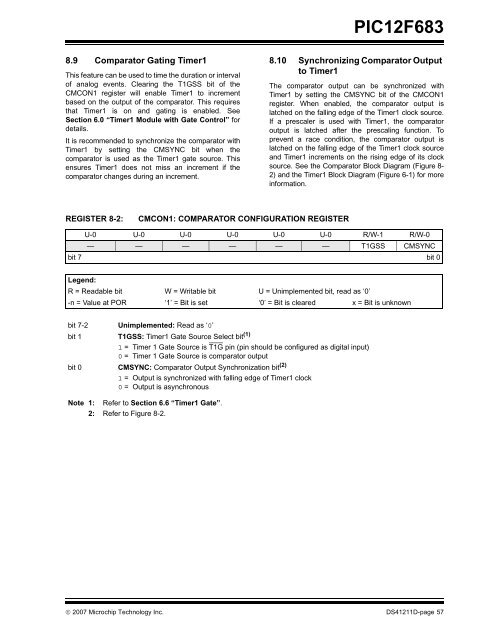
REGISTER 8-2:<br />
CMCON1: COMPARATOR CONFIGURATION REGISTER<br />
U-0 U-0 U-0 U-0 U-0 U-0 R/W-1 R/W-0<br />
— — — — — — T1GSS CMSYNC<br />
bit 7 bit 0<br />
Legend:<br />
R = Readable bit W = Writable bit U = Unimplemented bit, read as ‘0’<br />
-n = Value at POR ‘1’ = Bit is set ‘0’ = Bit is cleared x = Bit is unknown<br />
bit 7-2 Unimplemented: Read as ‘0’<br />
bit 1 T1GSS: Timer1 Gate Source Select bit (1)<br />
1 = Timer 1 Gate Source is T1G pin (pin should be configured as digital input)<br />
0 = Timer 1 Gate Source is comparator output<br />
bit 0 CMSYNC: Comparator Output Synchronization bit (2)<br />
1 = Output is synchronized with falling edge of Timer1 clock<br />
0 = Output is asynchronous<br />
Note 1: Refer to Section 6.6 “Timer1 Gate”.<br />
2: Refer to Figure 8-2.<br />
© 2007 <strong>Microchip</strong> Technology Inc. DS41211D-page 57


