

PIC12F683 Data Sheet - Microchip
PIC12F683 Data Sheet - Microchip
PIC12F683 Data Sheet - Microchip

You also want an ePaper? Increase the reach of your titles
YUMPU automatically turns print PDFs into web optimized ePapers that Google loves.
<strong>PIC12F683</strong><br />
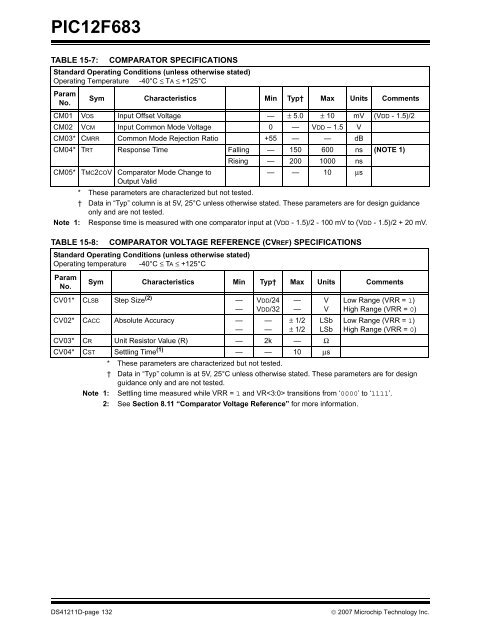
TABLE 15-7:<br />
TABLE 15-8:<br />
COMPARATOR SPECIFICATIONS<br />
Standard Operating Conditions (unless otherwise stated)<br />
Operating Temperature -40°C ≤ TA ≤ +125°C<br />
Param<br />
No.<br />
Sym Characteristics Min Typ† Max Units Comments<br />
CM01 VOS Input Offset Voltage — ± 5.0 ± 10 mV (VDD - 1.5)/2<br />
CM02 VCM Input Common Mode Voltage 0 — VDD – 1.5 V<br />
CM03* CMRR Common Mode Rejection Ratio +55 — — dB<br />
CM04* TRT Response Time Falling — 150 600 ns (NOTE 1)<br />
Rising — 200 1000 ns<br />
CM05* TMC2COV Comparator Mode Change to<br />
— — 10 μs<br />
Output Valid<br />
* These parameters are characterized but not tested.<br />
† <strong>Data</strong> in “Typ” column is at 5V, 25°C unless otherwise stated. These parameters are for design guidance<br />
only and are not tested.<br />
Note 1: Response time is measured with one comparator input at (VDD - 1.5)/2 - 100 mV to (VDD -1.5)/2+20mV.<br />
COMPARATOR VOLTAGE REFERENCE (CVREF) SPECIFICATIONS<br />
Standard Operating Conditions (unless otherwise stated)<br />
Operating temperature -40°C ≤ TA ≤ +125°C<br />
Param<br />
No.<br />
CV01* CLSB Step Size (2) —<br />
—<br />
CV02* CACC Absolute Accuracy —<br />
—<br />
Sym Characteristics Min Typ† Max Units Comments<br />
VDD/24<br />
VDD/32<br />
—<br />
—<br />
—<br />
—<br />
± 1/2<br />
± 1/2<br />
V<br />
V<br />
LSb<br />
LSb<br />
Low Range (VRR = 1)<br />
High Range (VRR = 0)<br />
Low Range (VRR = 1)<br />
High Range (VRR = 0)<br />
CV03* CR Unit Resistor Value (R) — 2k — Ω<br />
CV04* CST Settling Time (1) — — 10 μs<br />
* These parameters are characterized but not tested.<br />
† <strong>Data</strong> in “Typ” column is at 5V, 25°C unless otherwise stated. These parameters are for design<br />
guidance only and are not tested.<br />
Note 1: Settling time measured while VRR = 1 and VR transitions from ‘0000’ to ‘1111’.<br />
2: See Section 8.11 “Comparator Voltage Reference” for more information.<br />
DS41211D-page 132<br />
© 2007 <strong>Microchip</strong> Technology Inc.


