

PIC12F683 Data Sheet - Microchip
PIC12F683 Data Sheet - Microchip
PIC12F683 Data Sheet - Microchip

You also want an ePaper? Increase the reach of your titles
YUMPU automatically turns print PDFs into web optimized ePapers that Google loves.
<strong>PIC12F683</strong><br />
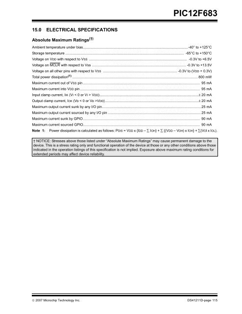
15.0 ELECTRICAL SPECIFICATIONS<br />
Absolute Maximum Ratings (†)<br />
Ambient temperature under bias..........................................................................................................-40° to +125°C<br />
Storage temperature ........................................................................................................................ -65°C to +150°C<br />
Voltage on VDD with respect to VSS ................................................................................................... -0.3V to +6.5V<br />
Voltage on MCLR with respect to Vss ............................................................................................... -0.3V to +13.5V<br />
Voltage on all other pins with respect to VSS ........................................................................... -0.3V to (VDD + 0.3V)<br />
Total power dissipation (1) ............................................................................................................................... 800 mW<br />
Maximum current out of VSS pin ...................................................................................................................... 95 mA<br />
Maximum current into VDD pin ......................................................................................................................... 95 mA<br />
Input clamp current, IIK (VI < 0 or VI > VDD)...............................................................................................................± 20 mA<br />
Output clamp current, IOK (Vo < 0 or Vo >VDD).........................................................................................................± 20 mA<br />
Maximum output current sunk by any I/O pin.................................................................................................... 25 mA<br />
Maximum output current sourced by any I/O pin .............................................................................................. 25 mA<br />
Maximum current sunk by GPIO...................................................................................................................... 90 mA<br />
Maximum current sourced GPIO...................................................................................................................... 90 mA<br />
Note 1: Power dissipation is calculated as follows: PDIS = VDD x {IDD – ∑ IOH} + ∑ {(VDD – VOH) x IOH} + ∑(VOl x IOL).<br />
† NOTICE: Stresses above those listed under “Absolute Maximum Ratings” may cause permanent damage to the<br />
device. This is a stress rating only and functional operation of the device at those or any other conditions above those<br />
indicated in the operation listings of this specification is not implied. Exposure above maximum rating conditions for<br />
extended periods may affect device reliability.<br />
© 2007 <strong>Microchip</strong> Technology Inc. DS41211D-page 115


