Diamond Detectors for Ionizing Radiation - HEPHY
Diamond Detectors for Ionizing Radiation - HEPHY
Diamond Detectors for Ionizing Radiation - HEPHY

You also want an ePaper? Increase the reach of your titles
YUMPU automatically turns print PDFs into web optimized ePapers that Google loves.
CHAPTER 8. DETECTOR GEOMETRIES 49<br />
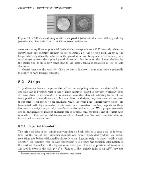
Figure 8.1: CVD diamond samples with a simple dot (substrate side) and with a guard ring<br />
(growth side). The scale ticks to the left represent millimeters.<br />
areas are the equilines of potential (each shade corresponds toa15Vinterval), while the<br />
arrows show the negative gradient of the potential, i.e., the electric eld. In total, the<br />
fringe eld is signicantly reduced by the guard structure, being restricted basically to a<br />
small range between the top and guard electrodes. Furthermore, the charges drained by<br />
the guard ring do no longer contribute to the signal, which is measured at the bottom<br />
electrode.<br />
Guard rings are also used <strong>for</strong> silicon detectors, however, the reason there is primarily<br />
to reduce surface leakage currents.<br />
8.2 Strips<br />
Strip detectors have a large number of narrow strip implants on one side, while the<br />
opposite side is provided with a single, large electrode, called backplane. Normally, each<br />
of these strips is wire-bonded to a separate amplier channel, allowing to detect the<br />
track position in one dimension. In some detector designs, only every second (or even<br />
third) strip is connected to an amplier, while the remaining \intermediate strips" are<br />
terminated with high impedance. As there is a capacitive coupling, signals on these<br />
intermediate strips are partially transfered to the readout strips. With proper geometric<br />
design, the number of readout channels can be dramatically reduced while only little SNR<br />
is sacriced. Strip and pixel detectors are often referred to as \trackers", as their intention<br />
is the track reconstruction.<br />
8.2.1 Spatial Resolution<br />
The principal idea of not simply applying dots on both sides is to gain position in<strong>for</strong>mation.<br />
At the cost of more amplier channels and more complicated readout, the spatial<br />
resolution gets better with smaller electrode areas, <strong>for</strong>ming strips or pixels. With a strip<br />
detector, the simplest case of data processing is to reduce the position in<strong>for</strong>mation to<br />
the readout channel with the highest observed signal. Thus, the position in<strong>for</strong>mation is<br />
digitized in steps of the strip pitch 1 p. Similar to the intrinsic noise of an ADC, one gets<br />
1 distance from one strip center to the neighbor strip center