Diamond Detectors for Ionizing Radiation - HEPHY
Diamond Detectors for Ionizing Radiation - HEPHY
Diamond Detectors for Ionizing Radiation - HEPHY

You also want an ePaper? Increase the reach of your titles
YUMPU automatically turns print PDFs into web optimized ePapers that Google loves.
Chapter 8<br />
Detector Geometries<br />
Usually solid state tracking detectors have metal electrodes on opposite sides, however<br />
the geometric layout varies considerably. This has implications on the electric eld distribution,<br />
the readout electronics and the spatial resolution.<br />
8.1 Dots<br />
In the simplest case, both electrodes are pads of equal size and shape at matching positions<br />
on either side. Thus, all induced charge from traversing particles is collected on<br />
the same electrode. In the diamond irradiation studies, the samples had circular pads<br />
with a diameter ranging from 1:8 to 5 mm. Although CVD diamond shows lateral inhomogeneities<br />
on a sub-millimeter scale, a pad area of 2:5mm 2 and more is large enough to<br />
average over the uctuations.<br />
As long as the particle track is close to the pad center, the charge is generated in a<br />
homogeneous electric eld, and the charge movement agrees with the model. Once the<br />
track hits the pad fringe, the electric eld is no longer homogeneous.<br />
For the diamond samples involved in the pion irradiation, the electric fringe eld has<br />
been numerically calculated and the mean eld strength has been computed on small<br />
ring elements. Together with the corresponding charge vs. electric eld plots (g. 5.4),<br />
the charge induced by hits in the area of the fringe eld could be obtained. Finally, the<br />
actual electric eld can be equivalently described by a sharp-edged homogeneous eld 40<br />
to 70% bigger than the pad area, depending on the sample geometry. However, as the<br />
charges follow the electric eld, they have to cross more grain boundaries in the fringe<br />
region than in the homogeneous part. This could to some extent reduce the resulting<br />
charge and thus the equivalent area, but has been neglected in these calculations.<br />
To avoid these complications, the samples can be equipped with a grounded guard<br />
ring electrode around the pad connected to the HV in order to restrict the fringe eld.<br />
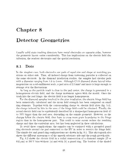
The simple dot and guard ring congurations are shown in g. 8.1. This photograph also<br />
shows the dierent appearances of the smooth substrate side and the rough growth side.<br />
Fig. 8.2 shows the electric eld in a radial cross-section of a diamond sample (D =<br />
641 m) at 300 V bias without (a) and with (b) a guard ring. The borders of the shaded<br />
48