Diamond Detectors for Ionizing Radiation - HEPHY
Diamond Detectors for Ionizing Radiation - HEPHY
Diamond Detectors for Ionizing Radiation - HEPHY

You also want an ePaper? Increase the reach of your titles
YUMPU automatically turns print PDFs into web optimized ePapers that Google loves.
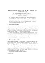
CHAPTER 5. DETECTOR MATERIAL COMPARISON 25<br />
eld is approximately constant throughout the bulk. Principally, the silicon detector is a<br />
wide-area diode.<br />
+<br />
p -implant<br />
y<br />
+<br />
n-type bulk<br />
n + -implant<br />
E<br />
Figure 5.5: Schematic cross-section of a silicon detector with implant thicknesses not to scale.<br />
The electric eld results from a bias voltage above the depletion voltage.<br />
Silicon detectors are made of very pure material, minimizing the number of charge<br />
traps and recombination centers. Nearly all charges excited in the bulk reach the electrodes,<br />
implying a charge collection eciency of (almost) 100%. According to the charge<br />
mobilities, the charge collection after a particle traversed the bulk takes a few nanoseconds.<br />
5.3 Ge <strong>Detectors</strong><br />
Germanium was the rst technically used semiconductor material. As the specic energy<br />
loss dE=dx is quite high in germanium compared to silicon, it better suits <strong>for</strong> calorimetry<br />
than <strong>for</strong> tracking purposes. For instance, lithium-drifted germanium detectors [26] with<br />
an active crystal volume of several cm 3 are used in nuclear spectroscopy. These detectors<br />
achieve an excellent energy resolution, however, they must be permanently cooled to<br />
liquid nitrogen temperature (T = 77 K). The low temperature not only conserves the<br />
arrangement of the lithium atoms inside the crystal, but also reduces the intrinsic carrier<br />
density dramatically. Only this fact permits the functioning of the device.<br />
Later, it became possible to produce extremely pure germanium material, which is<br />
more convenient to use. Still low temperature operation is essential, but an interruption<br />
of the cooling is no longer disastrous.<br />
5.4 GaAs <strong>Detectors</strong><br />
Gallium-arsenide is a III-V-type semiconductor. The semiconducting junction is introduced<br />
through a Schottky contact on the bulk material. Unlike silicon, the electric eld<br />
does not extend throughout the bulk [9], in fact, there is a passive layer with zero eld<br />
and the eld in the active layer is decreasing from a maximum at the Schottky contact to<br />
zero. Depending on the sample purity, there is a certain number of inter-band gap traps.<br />
Thus the charge collection eciency of the best samples is presently at the order of 50%<br />
to 80%.