Diamond Detectors for Ionizing Radiation - HEPHY
Diamond Detectors for Ionizing Radiation - HEPHY
Diamond Detectors for Ionizing Radiation - HEPHY

You also want an ePaper? Increase the reach of your titles
YUMPU automatically turns print PDFs into web optimized ePapers that Google loves.
CHAPTER 5. DETECTOR MATERIAL COMPARISON 24<br />
Collection Distance [µm]<br />
400<br />
350<br />
300<br />
250<br />
200<br />
150<br />
100<br />
10000<br />
5000<br />
Signal [e-]<br />
50<br />
Natural type IIa diamond<br />
1990 1992 1994 1996 1998<br />
Time [year]<br />
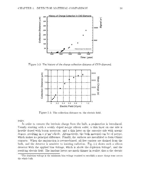
Figure 5.3: The history of the charge collection distance of CVD diamond.<br />
250<br />
Collection Distance (µm)<br />
200<br />
150<br />
100<br />
50<br />
8000<br />
6000<br />
4000<br />
2000<br />
Mean Charge (e)<br />
0<br />
0 0.2 0.4 0.6 0.8 1 1.2<br />
Electric Field (V/µm)<br />
0<br />
Figure 5.4: The collection distance vs. the electric eld.<br />
pairs.<br />
In order to remove the intrinsic charge from the bulk, a pn-junction is introduced.<br />
Usually starting with a weakly doped n-type silicon wafer, a thin layer on one side is<br />
heavily doped with boron acceptors, and a thin layer on the opposite side with arsenic<br />
donors, resulting in a p + nn + -diode. Alternatively, the bulk material can be of p-type,<br />
which makes no principal dierence. Finally, the surfaces are metallized to <strong>for</strong>m Ohmic<br />
contacts. When the pn-junction is reverse-biased, all free carriers are drained from the<br />
bulk, and the detector is sensitive to ionizing radiation. Fig. 5.5 shows such a silicon<br />
detector with the applied bias voltage, which is above the depletion voltage 1 , and the<br />
resulting electric eld. The implant layers are much thinner in reality, thus a the electric<br />
1 The depletion voltage is the minimum bias voltage required to establish a space charge zone across<br />
the whole bulk