Thin Films Deposition/Etch
Thin Films Deposition/Etch
Thin Films Deposition/Etch

Create successful ePaper yourself
Turn your PDF publications into a flip-book with our unique Google optimized e-Paper software.
<strong>Thin</strong> <strong>Films</strong><br />
<strong>Deposition</strong>/<strong>Etch</strong><br />
What thickness range defines <strong>Thin</strong> <strong>Films</strong><br />
To deposit, or etch, a thin film, a controlled<br />
environment is critical. What environment are<br />
most thin films deposited, or etched, in
Vacuum Science Review<br />
Objective – to reduce pressure in a chamber. At reduced<br />
pressures, a reduced number of gas molecules means the<br />
molecules will, on average, travel long distances before they<br />
collide with each other. This average distance is the mean free<br />
path (λ) and is inversely proportional to the pressure.<br />
! =<br />
kT<br />
2"d 2 P<br />
Ideal Gas Law: Model for a gas that assumes gas molecules are<br />
hard spheres that travel in straight lines until they collide<br />
P = nkT<br />
n = P<br />
kT<br />
where<br />
n: density of molecules (molecules/m 3 )<br />
P: pressure (Pa) 1 Pa = 1 N/m 2<br />
k: Boltzmanns constant (1.38 × 10 -23 J/ºK)<br />
Most traditional pressure unit used is Torr (pressure exerted by<br />
a Hg barometer column 1 mm in height → mm Hg)
At reduced pressures, reduced # gas molecules<br />
P (Torr) n (cm -3 ) Vacuum<br />
760 ∼10 19<br />
} Rough (0.1-760 Torr)<br />
1 ∼10 16<br />
} Medium (10<br />
10 -3 ∼10 -4 – 0.1 Torr)<br />
13<br />
10 -6 ∼10 10<br />
} High (10 -8 – 10 -4 Torr)<br />
10 -9 ∼10 7<br />
10 -12 ∼10 4 } UHV (< 10 -8 Torr)<br />
Many vacuum systems might use a mechanical pump to<br />
reduce the pressure to mTorr range (roughing pump)<br />
and then a high vacuum pump takes over to reduce<br />
pressure further.
Example<br />
Evaporation is typically performed at10 -6 Torr. What is λ for a<br />
pressure of 10 -6 Torr<br />
! =<br />
kT<br />
2"d 2 P<br />
At this pressure, a 4 Å diameter molecule has λ of:<br />
(1.38 ×10 -23 )(300)<br />
(√2)π (4×10 -10 ) 2 (10 -6 )(133.3)<br />
= 44 m.<br />
During evaporation, gas molecules essentially travel in a straight<br />
line from the evaporation source (crucible) to the substrate.<br />
Sputter deposition is typically performed at 10 -3 Torr. What is λ<br />
for sputter deposition
Pressure in a chamber is reduced by the use of vacuum pumps<br />
To keep conductance high,<br />
*keep tube as short as possible,<br />
*keep out bends, elbows,<br />
*keep tube diameter as large as possible<br />
A simple vacuum system showing a uniform pressure chamber with inlet<br />
flow Q, a vacuum pump, and a tube of conductance C.
Roughing Pumps<br />
Mechanical movement of a piston, vane, plunger…<br />
*capture a volume of gas<br />
*compression of the captured volume<br />
*gas expulsion<br />
One of the most common types of pumps for microelectronic<br />
processing is the rotary vane vacuum pump.<br />
A schematic of a single-stage, two-valve<br />
piston pump.
High Vacuum Pumps<br />
Diffusion: heat oil at bottom of pump; oil vapors<br />
rise through stack; ejected through vents at high<br />
speed; strike cooled walls, condense, and run down<br />
walls; gasses pumped by momentum transfer<br />
between vapor stream and gas molecules.<br />
Cutaway view of a diffusion pump (courtesy<br />
Varian).<br />
Cutaway view of a small turbomolecular pump. Notice<br />
the change in the blade angle and shape going from the<br />
high vacuum (top) to low vacuum (bottom) ends<br />
(courtesy Varian).<br />
Turbomolecular (turbo): large number of<br />
stages in series; each consists of a fan<br />
blade rotating at extremely high speeds<br />
(>20,000 rpm) and a set of blades called a<br />
stator; high rotation speeds makes them<br />
susceptible to mechanical problems.
High Vacuum Pumps<br />
(Entrapment)<br />
Cryopump (cryo): for ultimate in purity,<br />
consists of a cold head maintained at<br />
20K; Chamber gasses, except He, will<br />
condense on the cold head; eventually<br />
the cold head becomes saturated with<br />
adsorbed gasses and has to be<br />
regenerated (to desorb gases).<br />
Schematic view of a typical cryopump.<br />
Below 10 -6 Torr, outgassing is a major source of virtual<br />
leaks; load lock chambers useful for outgassing substrates.
Vacuum Seals and Pressure measurement<br />
Rough, medium: O-rings are used to seal; inexpensive, can reuse;<br />
elastomer material (VITON), a vulcanized rubber<br />
O-rings are placed in recessed areas (grooves) to keep the material<br />
from being pulled into chamber; can degrade if pumping highly<br />
toxic gases<br />
High, UHV: metal seals are used; Metal flanges: thick metal ring<br />
pinched between stainless steel edges.<br />
Pressure measurement:<br />
1) Capacitance manometers depend on pressure difference between chamber<br />
and reference; useful to about 100 mTorr<br />
2) Thermal conductivity (Pirani) pass current through a wire and measure Temp<br />
of wire – Resistance varies with Temp so is related to gas pressure; useful from<br />
mTorr to 1 Torr range<br />
3) Ionization gauges: hot filament ionizes gas; ions collected on an electrode that<br />
generate current ∝ ionization rate; used mTorr to 10 -8 Torr
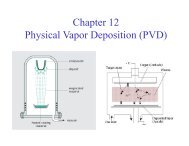
<strong>Thin</strong> Film <strong>Deposition</strong><br />
• Physical Vapor <strong>Deposition</strong> (PVD)<br />
1) Evaporation<br />
E-beam, thermal<br />
2) Sputter deposition<br />
• Chemical Vapor <strong>Deposition</strong> (CVD)<br />
1) Atmospheric (APCVD)<br />
2) Low pressure (LPCVD)<br />
3) Plasma Enhanced (PECVD)
Evaporation – condensation of a metal vapor on substrate; metal pieces<br />
are placed in a crucible and heated to the melting point (or an electron beam<br />
heats them). This process is done at low pressure (long mean free path). This<br />
process results in high purity films but is unable to cover severe steps.
<strong>Deposition</strong> rate depends on position of wafer<br />
View factor, k depends on R, Θ, Φ<br />
Wafers directly above the crucible will be coated more heavily than<br />
wafers off to the side. Wafers can all be mounted on the surface of a<br />
sphere (planetary) for more uniform deposition.<br />
Figure 12.3 The geometry of deposition for a wafer (A) in an arbitrary<br />
position and (B) on the surface of a sphere.
Step Coverage<br />
If the substrate surface is not<br />
planar, the long mfp (λ) in<br />
evaporation means that<br />
evaporated material will follow<br />
a straight line; some areas are<br />
shadowed<br />
Aspect Ratio<br />
AR = step height<br />
step diameter<br />
Helps to rotate and heat the<br />
substrates.<br />
Planetary holders rotate<br />
simultaneously around two<br />
axes.<br />
(A) Time evolution of the evaporative coating of<br />
a feature with aspect ratio of 1.0, with little<br />
surface atom mobility (i.e., low substrate<br />
temperature) and no rotation. (B) Final profile of<br />
deposition on rotated and heated substrates.
Thermal Evaporation<br />
1) Resistively heated<br />
Resistive evaporator sources. (A) Simple sources including heating the charge itself and using a coil of refractory<br />
metal heater coil and a charge rod. (B) More standard thermal sources including a dimpled boat in resistive media.<br />
2) Inductively heated<br />
Example of an inductively heated crucible used to create moderately charged temperatures.
Electron Beam Evaporation<br />
Heat of vaporization is<br />
supplied by the impact of<br />
an electron beam that<br />
melts a region of the<br />
material to be evaporated;<br />
Adv: possible to coevaporate<br />
materials with<br />
dual crucibles<br />
Disadv: more expensive<br />
than resistance heated<br />
systems, substrates may<br />
have radiation damage<br />
Electron beam evaporative sources. (A) A simple low flux source using a<br />
hot wire electron source and a thin movable rod. (B) A popular source using<br />
a 2707 source arc in which the beam can be rastered across the surface of<br />
the charge. The magnet must be much larger than shown to achieve the full<br />
270° of arc.
Evaporation<br />
Advantages: Simple process, relatively<br />
inexpensive, high purity films can be<br />
deposited.<br />
Disadvantages: difficult to evaporate alloys<br />
due to different melting points, line of<br />
sight deposition results in poor surface<br />
coverage unless there is rotation of the<br />
samples; deposition of refractory materials<br />
is a problem due to high temperatures<br />
required.<br />
A commercial evaporator. Inset shows a<br />
planetary (photographs courtesy of CHA<br />
Industries).
Sputtering –involves the acceleration of ions, usually Argon, through<br />
a potential gradient and the bombardment of these ions of a target<br />
material (cathode). Wafer surface is the anode. This process is<br />
good for sputtering alloys (the “target” can be made with a specific<br />
composition of the material you want to deposit).<br />
Material is<br />
sputtered from the<br />
target and deposited<br />
on the wafer;<br />
Plasma: partially ionized<br />
gas; used to create reactive<br />
atmospheres.
Sputter Yield (S)<br />
Determines rate of sputter deposition<br />
S = # target atoms ejected/number of<br />
ions incident<br />
Depends on:<br />
• Target material<br />
• Mass of bombarding ions<br />
• Energy of bombarding ions<br />
Each target material has a threshold<br />
energy (below that energy no<br />
sputtering occurs), typically 10-30 eV.<br />
Sputter yield as a function of ion energy for<br />
normal incidence argon ions for a variety of<br />
materials (after Anderson and Bay, reprinted by<br />
permission).
Magnetron Sputtering – a magnetic field applied at right angles to<br />
the E-field; causes e- to follow spiral paths, increases probability of<br />
ionizing a gas atom, increases ionization efficiency, confines<br />
plasma resulting in a higher deposition rate; also able to form<br />
plasma at lower chamber pressures<br />
Planar and cylindrical magnetron sputtering systems T: target; P: plasma; SM:<br />
solenoid; M: magnet; E: electric field; B: magnetic field (after Wasa and<br />
Hayakawa, reprinted by permission, Noyes Publications).
Step Coverage<br />
Application of substrate heat will dramatically improve the step<br />
coverage due to surface diffusion; High AR can be a problem<br />
otherwise.<br />
Cross section of the time evolution of the<br />
typical step coverage for unheated sputter<br />
deposition in a high aspect ratio contact.<br />
Sputtering<br />
Advantages: Moderately good step coverage; preferred technique<br />
for deposition of alloys, can sputter a wide variety of materials.<br />
Disadvantages: may have some Argon incorporation in the film;<br />
could have some damage to substrate although not as much as in e-<br />
beam evaporation.
CVD –uses chemical reactions in the gas phase that result in thin film<br />
deposition on a wafer.<br />
A simple thermal CVD reactor.<br />
Simple continuous-feed atmospheric pressure<br />
reactor (APCVD).
Film deposition is highly temperature dependent<br />
<strong>Deposition</strong> rate of polysilicon as a function of temperature and of<br />
silane flow rate (after Voutsas and Hatalis, reprinted by<br />
permission of the publisher, The Electrochemical Society).
PECVD: Use of a<br />
plasma allows one to<br />
bring down the<br />
temperature for wafers<br />
that might be more<br />
temperature sensitive.<br />
Quality of film is lower<br />
than when grown at<br />
higher temperatures.<br />
Basic PECVD geometries: cold wall<br />
parallel plate, hot wall parallel plate,<br />
and ECR.
Chemical Vapor <strong>Deposition</strong><br />
Advantages: Standard furnace configurations<br />
provide high throughput and good film<br />
uniformity. Excellent step coverage.<br />
Disadvantages: Complicated process with need<br />
to control chemical reactions although commonly<br />
used materials for semiconductor applications are<br />
well known. If deposition isn’t properly<br />
controlled (solids formed only at the wafer<br />
surface), solids can be formed in the gas phase<br />
and result is the inclusion of particles in the thin<br />
film.<br />
Profiles of SiO 2 deposited by<br />
(A) PECVD, (B) thermal<br />
CVD, and (C) HDP CVD<br />
(courtesy IBM).
Sputtering, evaporation, and CVD are deposition techniques that<br />
can produce radically different films. One particular difference is<br />
in the film conformality, or ability to uniformly coat different<br />
morphologies. Please match the deposited film depicted<br />
schematically below with the method used to deposit it.
<strong>Thin</strong> Film <strong>Etch</strong>ing<br />
After photoresist image is formed, need to ETCH material away in<br />
places not protected by photoresist. Until the film to be<br />
patterned is etched, you have only a patterned PR.<br />
<strong>Etch</strong> Processes:<br />
1) Wet chemical etching – immersion of wafers in chemical bath<br />
2) Dry plasma etching – vacuum system with inert or reactive gas<br />
Parameters of interest:<br />
1) <strong>Etch</strong> rate (ER); measured in film thickness/time;<br />
<strong>Etch</strong> Rate Uniformity (% variation of etch rate; measured across a<br />
wafer and wafer to wafer)<br />
2) Selectivity = (ER material of interest)/(ER mask material<br />
3) Undercut (lateral etch underneath mask material)
Wet etching is isotropic and produces cross sections with<br />
not very vertical sidewalls. <strong>Etch</strong> bias is the difference in<br />
etch feature size and printed feature size.<br />
Isotropic <strong>Etch</strong><br />
Occurs in all<br />
directions<br />
equally<br />
Typical isotropic etch process showing the etch bias.
Undercut is described by etch anisotropy, A = 1 – R L /R v<br />
Where R L : lateral ER and R v : vertical ER<br />
A = 1 if R L = 0 so perfectly anisotropic<br />
A = 0 if R L = R v ; lateral and vertical ER identical<br />
Over etching in an isotropic etch can be catastrophic; can result in<br />
lifting away of PR completely.<br />
Wet etching<br />
- purely chemical process<br />
- isotropic<br />
- particle contamination (etched materials are in the etchant solution)<br />
- highly selective<br />
- does not damage substrate<br />
- not practical for etching fine features but is still used where the<br />
isotropic nature can be tolerated
Wet Techniques<br />
For uniform, controlled etches, the etchant solution is often agitated<br />
to assist in moving etchant all over surface; this is typically done in<br />
an ultrasonic bath or by a continuous acid spray<br />
Wet Bench at U Arkansas<br />
(left); cassette of 300 mm<br />
wafers (right) by SCP<br />
Global Technologies;<br />
Megasonic Tank<br />
(bottom).
Dry etching is anisotropic and produces cross sections<br />
with very vertical sidewalls.<br />
Plasma <strong>Etch</strong>ing<br />
Ion Milling<br />
Reactive Ion <strong>Etch</strong> (RIE)<br />
These etch processes are done under vacuum.<br />
• Plasma etching (0.1 – 100 Torr);<br />
• Ion milling (10 -3 to 10 -5 Torr) uses Ar ions to<br />
etch material;<br />
• RIE uses RF power (1-100 mTorr) in a<br />
reactive gas environment (Cl or F based).<br />
Tradeoffs between selectivity and anisotropy
Lift-off processing (pattern<br />
materials that are not easily<br />
etched) - The substrate is covered<br />
with photoresist first; the PR is<br />
patterned and then the film to be<br />
patterned is deposited over the<br />
surface. Finally the PR is removed<br />
and any material deposited on top<br />
of the PR will be removed with the<br />
resist.<br />
I.<br />
II.<br />
III.<br />
IV.<br />
9/27/12 11:20 AM<br />
1<br />
2<br />
1<br />
2<br />
1<br />
3<br />
2<br />
1<br />
Key difference: Pattern PR<br />
before applying film to<br />
be patterned – PR acts<br />
as your “stencil”<br />
V.<br />
file:///Users/sburkett/Desktop/Teaching/Classes/ECE-493/Lectures/Lift-off.svg<br />
2<br />
3<br />
Page 1 of 2